Module 01
Introduction to Semiconductors
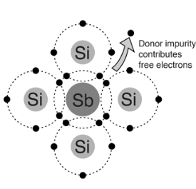
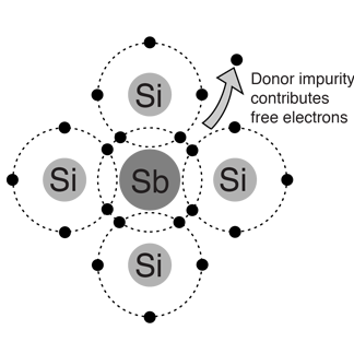
N type Semiconductor:-
To increase the number of conduction band electrons inintrisic silicon , pentavalent imparity atoms are added. these are atoms with five valence electrons such as
i) arsenic (as)
ii) phosphors (p)
iii) Bismuth (Bi)
iii) Antimony ( sb)
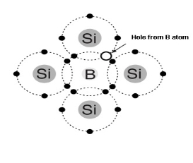
P Type Semiconductor :-
To increase the number of holes in intrinsic silicon trivalent impurity atoms are added these are atoms with their valence electrons such as
i) Baron(B)
ii) Indium(IN)
iii)Gallium(GO)
V Barrier
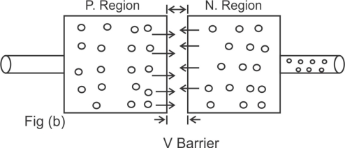
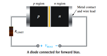
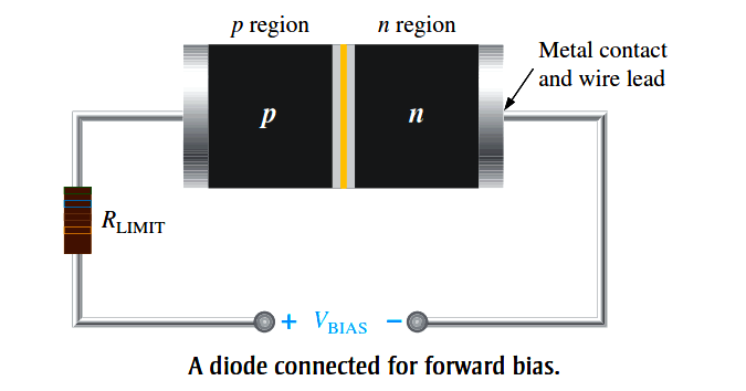
The effect of forward bias on the depletion region:-
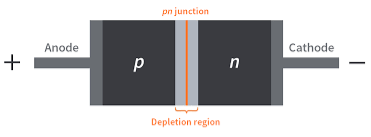
Depletion Region
The Effect of the Barrier Potential during forward bias:-
REVERSE BIAS:-
Reverse bias is the condition the essentially prevents current through the diode.
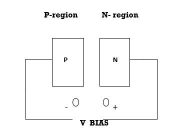
A Diode connected for Reverse Biased-


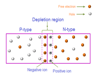
- As more of the N & P regions become depleted of majority carriers, the electric field between the positive and -ve ions increase in strength the depletion region equals the bios vtg .this point the transition current essentially ceases except for a small reverse current that can usually be neglected.
Reverse Current
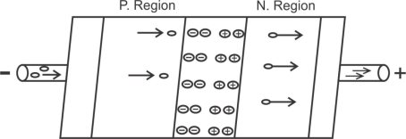
The Extremely small reverse current in a reverse biased diode is due to the minority carriers from thermally generated
e=hole pairs
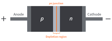
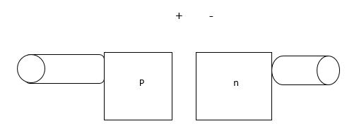
The Diode - Before doping the p-type & N-type consisting silicon material atom acting as a neutral.
IF a piece of intrinsic silicon is doped so that part is n-type and the other part is p-type, a junction forms at the bounded between the two regions and a diode is created.
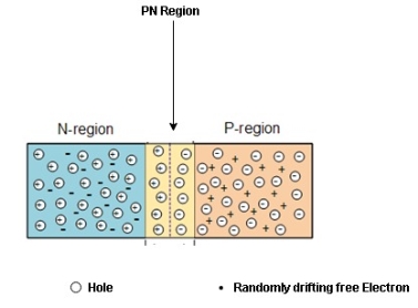
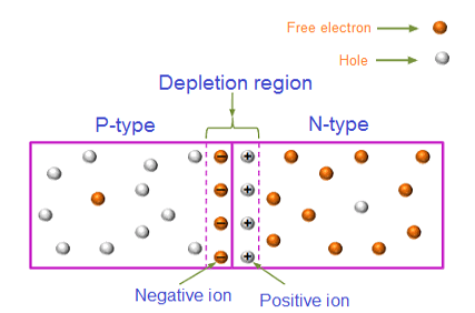
Formation of the Depletion Region
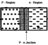
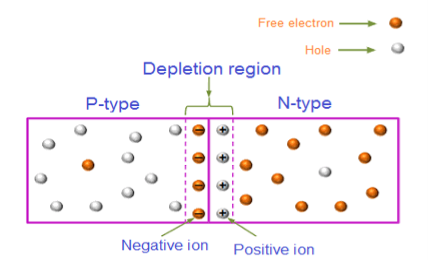
For every electron that defuse across the junction and combines with a hole , a positive charge is left in the region and a ve charge is created in the p-region firming a barriers potential. This action continues until the vtg of the barrier ripples further diffusion.
The Depletion region acts as a barriers to the farther movement of electrons across the junction
As positive ion & -ve ion across the junction produces a electric field across the junction -according to coulombs law.
The potential difference of the electric field across the depletion region is the amount of vtg required to move electronics through the electric field, this potential difference is called the barrier potential & is expressed in volt
The typical barrier potential is approximately 0.7 v for silicon & 0.3 v for germanium at 25c.
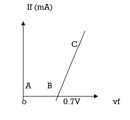
A :- v=A Characteristic for forward bias:-
V-I Characteristics:-
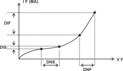
Graph shows how the dynamic resistance decrease as we move up the curve xd= DNF/DIF=
As we continue to increase the forward bias voltage the current continues to increase very rapidly ,but the voltage across the diode increase only gradually above 0.7 v.
This small increase in the diode vtg above the barrier potential is due to the voltage drop across the internal dynamic resistance of the semi conductive material.
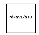
Dynamic resistance:- A Resistance change as move along a V-I curve it is called dynamic or A. C resistance.
B) V - I Characteristics for Reverse biased :-
When the applied bias voltage is increased to a value where. the reverse vtg across the diode the reaches appropriately 0.7 v (barrier potential) the forward current begins to increase rapidly.
As we continue to increase the bias voltage the current continues to increase very rapidly bit the voltage across the diode increases very little above VBR.
IR increases little above VBR. resulting in overheating & possible damage.
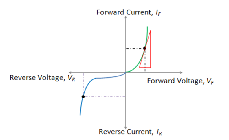
Static or DC Resistance
It is the resistance offered by the diode to the flow of DC through it when we apply a DC voltage to it. Mathematically the static resistance is expressed as the ratio of DC voltage applied across the diode terminals to the DC flowing through it (shown by the black dotted line in Figure) i.e.
Dynamic or AC Resistance
It is the resistance offered by the diode to the flow of AC through it when we connect it in a circuit which has an AC voltage source as an active circuit element. Mathematically the dynamic resistance is given as the ratio of change in voltage applied across the diode to the resulting change in the current flowing through it. This is shown by the slope-indicating red solid lines in Figure and is expressed as

 ampers
Where ,
V= Applied voltage across the diode in volts
I=Current flow through the diode in amperes.
n= 2 for silicon P-N junction diode
=1 for germanium P-N junction diode.
IO = reverse saturation current flow through diode in amperes.
VT =Is the voltage equivalent of temperature in volts.
VT= K X T volt’s
K=Boltzmann's constant
K=8.62 * 10 -s ev/k
I= temperature in ok
The equation VI= K * T indicates that the current flow through the diode also depend upon the ambient temperature.
Room temperature =25 0c
T= 273+25=298K
VT=K * T


i) Avalanche breakdown:-As the magnitude of the reverse bias vtg is increased the kinetic energy of the minority carriers gets increased. while travelling the minority carriers collide with the stationery atoms which in turns results in breaking some of the covalent bond & generating free e- (carrier multiplication)
This process continues leading to a very swift multiplication giving rise to a large reverse current in just a few picoseconds. this effect is called as avalanche breakdown effect.
Topical Breakdown vtg is about 50v to 100v:-
i) Due to large power dissipation the junction temperature increase & may destroy the semiconductor device permanently.
ii) Zener Breakdown: - This type of breakdown occurs in heavily doped P-N junction in which the depletion region is very narrow.
All the applied reverse voltage appears across the depletion layer. the electric field is vtg per unit distance. it is very intense at the depletion region.
There for it can pull the electronic out of the valance bond by breaking the covalent bonds and producing the free electrons. This process is known as zener effect.
Due to this heavy current flow & diode may damage.
PRINCIPLE OF OPERATION: - A zener diode can be forward biased or reverses biased. its operation in the forward biased mode is same as that of a p-n junction diode but its operation in the reverse biased mode is sustainably deferent.


Numerical:
A 5.0V stabilized power supply is required to be produced from a 12V DC power supply input source. The maximum power rating PZ of the zener diode is 2W. Using the zener regulator circuit above calculate:
a). The maximum current flowing through the zener diode.
Maximum current = Watts/ Voltage =2W/5V =400mA
b). The minimum value of the series resistor, RS
 = 17.5 Ω
c). The load current IL if a load resistor of 1kΩ is connected across the zener diode.

d). The zener current IZ at full load.
Iz =Is -Il =440mA – 5mA = 395mA
Half Wave rectifier
1) Due to the unidirectional current flow through the transformer there is a possibility of core saturation to avoid this transformer size must be increased.
2) Ripple factor is high.
3) Low rectification effecting.
4) Law TUF.
5) Law D.C O/P VTG & current.
6) Large filter component are required.
ADVANTAGES:-
1) Simple Construction.
2) Component required less.
3) Small size.
APPLICATION:-
Walkman, law cost power supply.
TRANSFORMER UTILISATION FACTOR (TUF):-It indicates how well the ilp transformer is being utilized
TUF= DC O/P Power / AC power rating of the transformer

Full Wave Rectifier
1) A centre tapped rectifier is a type of full wave rectifier that uses two diode connected to the secondary of a centre tapped transformer.
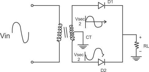
Center tapped full wave rectifier operation:-
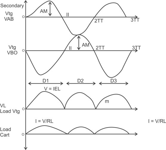
I) During positive half cycle of i/p ac supply.
Diagram

D1.Is in forward biased & D2 is in reverse biased.
II)During -ve half cycle.

D1 Reverse biased
D2 Forward biased
ADVANTAGES
1) law ripple factor as Compared to HKR.
2)Better rectification efficiency.
3) Better TUF.
4)Higher value of average load vtg & avg load crt.
5)No possibility of transformer core saturation.
DISADVANTAGES
PIV of diode is 2vm , more size costly.
APPLICATION
I) Battery charges.
2)power supply at laboratory, high current, electronic ckt.
Diode C kts called limiters or clippers are sometimes used to clip off portions of signal voltages above or below certain levels.
Another type of diode ckt called a clamper is used to add or restore a d.c level to an electrical signal.
Below fig a) that limits or clips the positive part of the input voltage As the ilp vtg goes positive the diode become forward biased Because the cathode is at ground potential (ov)the anode cannot exceed 0.7v (for si)
So point A is limited to 0.7v the diode is reverse biased and appears as an open. The O/P VTG looks like the with a magnitude determined by the voltage divider formed by R1& the load resistor RL.
Vout=(RL/R1+RL) vin
If R1 small compared to RL then vout = vin

Clipper of the positive alternation. The diode is F,B during the +ve alternate RB during –ve alternation:-

Limiting of the negative alternation the diode is PB during the –ve alternation R.B during the +ve alternation.
During Reverse bias the +ve part of the ilp vtg is clipped off when the diode is forward biased during the –ve part of the ilp vtg is clipped off. when the diode is F.B during the –ve part of the ilp vtg point A is held at 0.7v by the diode is no longer forward biased and a voltage appears across RL proportional to the ilp vtg.
Problem:- What would you expect to see displayed on oscilloscope connected across RL in the Limiter.

The diode is forward biased and conducts when then the i/p vtg goes below -0.7v so for the –ve limiter , the peak o/p vtg across RL can be determined by the following
Equation -
Volt =(RL/R+RL) Vin
=(1k/100+1k)10v
= 1K/1.1K*10
=1*103/1.1*103*10
= 1*104/11*102*10
= 1*104*10-2*10
=10/11 10*10*10/11
Volt = 10000/11 = 9.09V
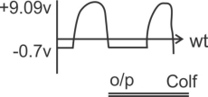

The voltage at point A mast equal VBINS+0.7v before the diode will become forward biased & conduct
Once the diode begins to conduct the vtg at point A is limited to VBINS +0.7 so that all ilp above this level is clipped off

To limit a vtg to a specified –ve level the diode & bios vtg must be connected. In this case the vtg at point ‘A’ must go below –VBIN-0.7v to forward biased the diode & initiate limiting action
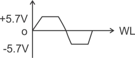
Prob:- fig shows a ckt combing a positive clipper with a-ve clipper .Determine the o/p vtg c/f

When the voltage at point A riches +5.7V diode A conducted and limits the waveform to +5.7v diode D2 does not conduct until the voltage reaches -5.7V
Therefore positive voltages above +5.7V & -ve voltages below -5.7V are clipped off
1) Positive Clamper:-
Diagram:-

Assumptions :-
1) The V/p is a perfect sine waveform
2)The value of R& C are chosen such that the Line constant T=RC is large equal
3)The diode is an ideal one
4)The Rc time constant is much longer as compared to one cattle period ‘T’ of the input.
RC >100T

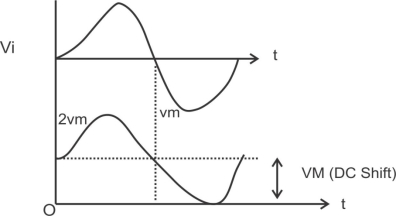
The diode reverse biased in both half cycle so it remains off.
2)Negative Clamper:-

In the first positive half cycle the capacitor will charge through the forward biased to peak vtg vm
The charging takes place very quickly as the diode resistances negligibly small
Once the capacitor charges to vm the diode is reverse biased and stops conducting.

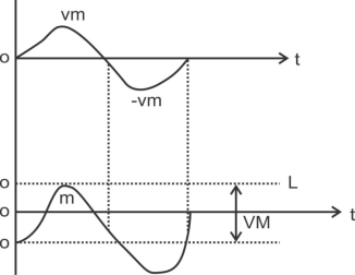
Diagram non ideal diode
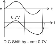
diagram:-
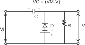
-Clamper with additional dc source:-
Diagram-
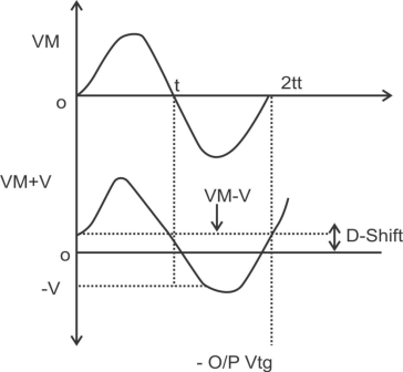
The load vtg W/F shows d.c level shift is positive but less than +vm
Level shift is given by
DG shift = vm - v
In the –ve half cycle ilp the diode will be forward biased and capacitor gets charged to a vtg (vm-v) volts with the polarities shown.
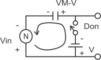
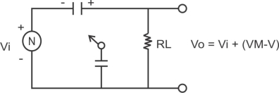
In above diagram during positive half cycle diode will remain permanently off therefore .the job of the diode is only to charge the capacitor.
Vo=vc +vi
Vo=(vm-v)+vi
1)Series Negative clipper :- Ideal diode
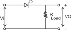
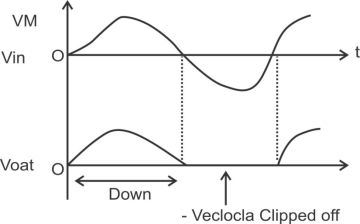
In the positive half cycle of the sinusoidal ilp the diode is forward biased. Being an ideal diode , it acts as a closed switch & connects the load across the ilp the load vtg there fore equal to the ilp vtg in the positive half cycle.
In the –ve half cycle of the diode is reverse biased acts as an open ckts/w the load vtg is therefore zero during the –ve half cycle.
2) Series Positive clipper:-

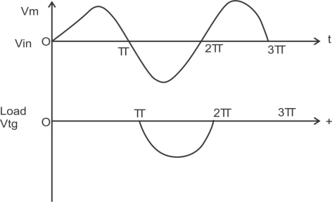
1) Biased Series – ve Clipper:-
2)

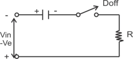
The operation of this ckt can be divided in to there intervals
1) Operation when in is +ve but less than v:-in the positive half cycle of the ilp as long as vin v the diode is not forward biased, therefore from to and then from t2 to t/2 shown in fig below the diode will remain in off state and the o/p voltage will be zero.

Fig -a) Equivalent ckt for +vin>v -
-

Fig b) Equivalent ckt for vin -ve
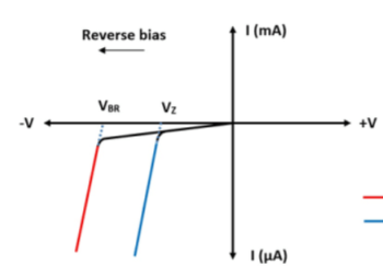
An avalanche diode is a type of semiconductor diode which is designed to experience avalanche breakdown at a specified reverse bias voltage. The pn junction of an avalanche diode is designed to prevent current concentration and resulting hot spots so that the diode is undamaged by the avalanche breakdown.
The avalanche breakdown that occurs is due to minority carriers accelerated enough to create ionization in the crystal lattice, producing more carriers which in turn create more ionization. Because the avalanche breakdown is uniform across the whole junction, the breakdown voltage is nearly constant with changing current when compared to a non-avalanche diode.
The construction of the avalanche diode is similar to the Zener diode, and indeed both Zener breakdown and Avalanche breakdown are present in these diodes. Avalanche diodes are optimized for avalanche breakdown conditions, so they exhibit small but significant voltage drop under breakdown conditions, unlike Zener diodes that always maintain a voltage higher than breakdown.
This feature provides better surge protection than a simple Zener diode and acts more like a gas discharge tube replacement. Avalanche diodes have a small positive temperature coefficient of voltage, where diodes relying on the Zener effect have a negative temperature coefficient.
The normal diode allows an electric current in one direction i.e. forward direction. Whereas, avalanche diode allows the current in both direction i.e. forward and reverse direction but it is specially designed to work in reverse bias condition.
BJT:- The BJT is constructed with the three draped semiconductors region’s separate by two PN junctions as shown below
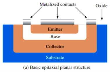
-Basic epitaxial planner structures.
-Three terminal with region’s are called emitter, base and collector.
-The physical representation of the two types of BJT’s,
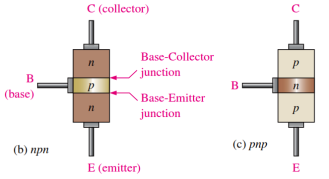
One type consists between two regions separated by a P region (npn) and other type consists of two p regions separated by an n region (pnp).
-The Pn junction joining the base region and the emitter region is called the base emitter junction.
-The Pn junction joining the base region and the collector region is called the base collector junction.
-The base region is lightly doped and very thin compared to the heavily doped emitter and the moderately doped collector regions.
*Base Transistor Operation:-
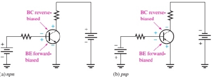
In order for the transistor to operate properly as an amplifier the two pn junction must be correctly biased with the external D.C vtg.
-The next figure shows the proper bias arrangement for both the npn and pnp transistors for active operation as an amplifier.
-In both the cases the base emitter
(BE) junction is forward biased & the base collector junction (BC) junction is reverse biased
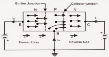
Current Equation in n-p- n, p-n-p transistors & amplifier
Transistor Current:-
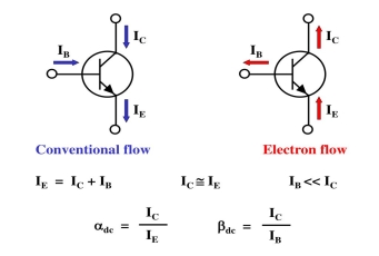
Transistor’s Characteristic’s and parameters: -
-The transistors is connected to d.c bias vtg for both the npn&pnp types VBB forward biases the base emitter junction &Vcc reverse biases the base collector junction.
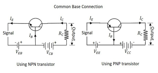
*Biasing conditions for different regions of operation:-
Sr. no | Region of operation | BE junction | CB junction | work |
1 | Cutoff region | R.B | R.B | S/w |
2 | Active region | F.B | R.B | Ampr |
3 | Saturation region | F.B | F.B |
|
Transistor’s Configuration:-
1) Common Base configuration(C.B)
2) Common emitter Configuration(C.E)
3) Common Collector Configuration(C.C)
Common Base configuration(C.B):-

-The I/p is applied between the emitter and the base. The base acts as a common terminal between the I/p and o/p.
-The input vtg is therefore VEB and the input current is IE.
-The output is taken between the collector and the base therefore the output vtg is VCB and the output current is IC.
* Current relation’s in CB configuration:-
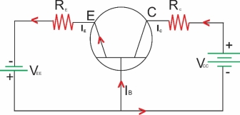
-The collector current is IC of the common base configuration is given by
Ic=Ic(INI)+ICBO
-Where the Ic(INI) called the injected collectors current and it is due to the number of electrons crossing the collectors base junction.
-ICBO :- This is the reverse saturation current flowing due to the minority carrier’s between the collector and base when the emitter is open
-ICBO flow’s due to the reverse biased collector’s base junction. As ICBO negligible as compared to Ic(INI) we can neglect it in practice.
.’. Ic=Ic(INI)………………………practically
Ic=ICBO………………with emitter open
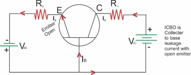
 Emitter is open
 ICBO
ICBO
Collector is to base control
-Since the ICBO flow’s due to terminally generated minority carrier’s it increases with increase the temperature.
-It doubles it’s value for every 100c rise in temperature.
-Current amplification factor or current gain (ddc):-
Current amplification factor or current gain is the ratio of collector current due to the injection to the total emitter current
αd.c = Ic(INI)
-The value of the ddc for CB configuration will always be less than 1.This is because
Ic(INI)<IE.
-Typically the value of d.d.c ranges between 0.95 to 0.995 depending upon the thickness of the base region.
-Larger the thickness of the base region smaller the value of the d.d.c
Ic(INI)=d.d.c.IE
Hence the expression for IC is given by
IC=αd.c IE + ICBo--------------------I
But the ICBo is negligibly small
IC d.d.c IE
* Expression for IB:-
IE=IB+IC
IE=αd.cIE+ICBo+IB…………………from I
IB=(1-αd.c)IE-ICBo
Neglecting ICBo
IB=(1-αd.c)IE
1. Input Characteristic:-
A. Input Characteristic: is always a graph of input current verses input vtg. For common base (CB) configuration input current is the emitter current (IE) & I/p vtg. is the emitter to the base vtg (VEB)
The I/p Characteristic is plotted at a constant O/p vtg. VCB
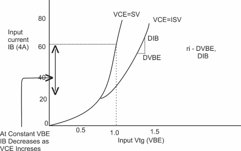
B. Output Characteristic:
Output Characteristic is always a graph of O/p current versus O/p Vtg.
For the CB configuration the O/p current is collector current (IC) of the output voltage is collector to base vtg. (VCB)
Output Characteristic is plotted for a constant value of I/p current (IE)
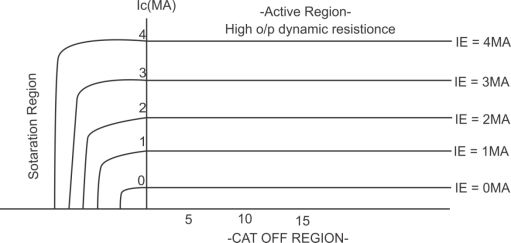
O/p Characteristic of a n-p-n transistor in CB Configuration
Dynamic O/p resistance (ro)
ro =  / I
/ I  constant
in the active region Ic does not depend on VCB. It depends only on the I/p current IE. That is why the transistor is called as a current controlled or current operated device.
Feature of CB configuration :

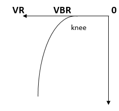
Fig.: DC Load Line (Ref. 2)


Fig.: DC Load Line characteristic curve (Ref. 2)

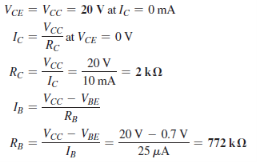
Numerical
Determine the values of VCC RC and RB of a fixed bias configuration for a given load line and defined Q point.

Solution:
Base bias is the simplest way of biasing a BJT transistor. It ensures that the voltage applied at the base, VBB, is correct, which then supplies this current so that the BJT has enough base current to switch on the transistor.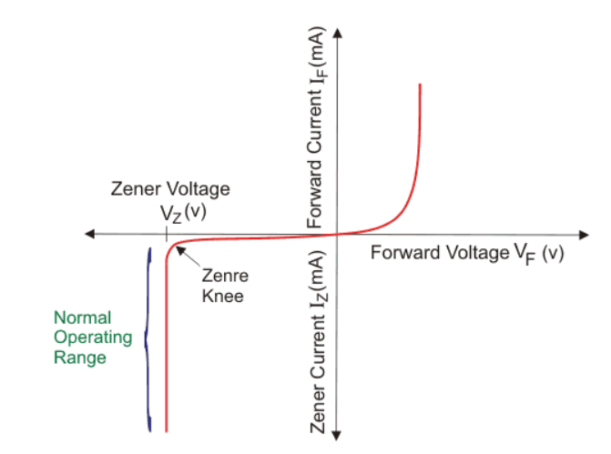
VBB is used to provide sufficient current to turn on the transistor. RB is used to provide the desired value of base current IB. VCC is the collector supply voltage required for a transistor to have sufficient power to operate. This voltage, reverse-biases the transistor, so that the transistor has sufficient power to have an amplified output collector current. The collector resistor, RC provides the desired voltage in the collector circuit
The base current is found by dividing the voltage across resistor RB shown below:
IB= (VBB - VBE)/RB
Since the voltage drop across a silicon junction is 0.7V, the value of VBE=0.7V. Therefore, IB equals:
IB= (VBB - VBE)/RB= (5v - 0.7v)/56kΩ= 76.78µA
The collector current IC can be calculated next:
IC=βdc x IB= 100 x 76.78µA≈ 7.68mA
With IC then known, the collector-emitter voltage, VCE can be calculated.
VCE= VCC - IC x RC= 15v - (7.68mA x 1KΩ)= 7.32v
Base biasing can also be done with a single supply voltage, VCC, omitting VBB. So instead of using VBB in calculations, you use VCC. The result of the calculations remains the same.
Disadvantages:
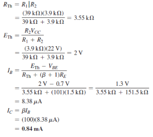
Voltage divider bias
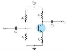
Fig.: Voltage Divider Bias (Ref. 2)
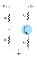
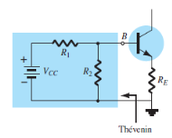
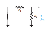
Fig.: Analysis of Voltage Divider circuit (Ref. 2)


Put IE = ( β + 1 ) IB


Numerical
Determine dc bias voltage VCE and current IC for voltage divider configuration. (Ref. 2)
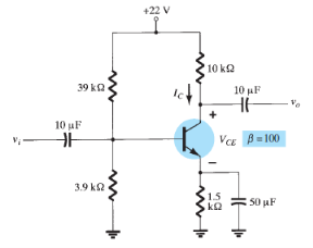
Solution:
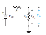
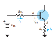

References:
1. Electronic Devices Circuit Theory - by Rober L. Boylestad 11th Edition, Pearson Publication, 2014
2. Microelectronic Circuits by A. S. Sedra and Kenneth C. Smith 7th Edition, Oxford University Press. 2017
3. Digital Design by M. Morris Mano, 5th Edition, Pearson Publication, 2016.