Module 02
Field Effect Transistor

Operation
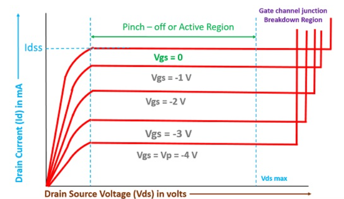
I-V characteristics
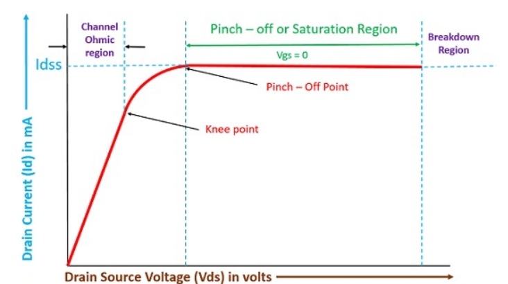
Output Characteristics or Drain Characteristics
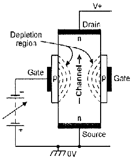
2. With external bias: When the external bias is applied to the gate-source terminal, the gate-source terminal becomes reversed bias externally. Obviously, if we are supplying an external voltage, then we can achieve the pinch-off point quite early as compared to the circuit which is not biased.
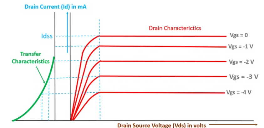
Transfer Characteristics
The transfer characteristics can be determined by observing different values of drain current with variation in gate-source voltage provided that the drain-source voltage should be constant. The transfer characteristics are just opposite to drain characteristics.
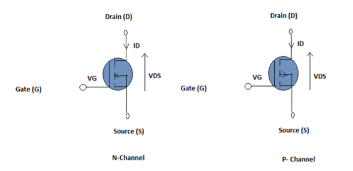
Operation
Function:
When there is no voltage on the gate, the channel shows maximum conductance. When the voltage on the gate is either positive or negative, the channel conductivity decreases.
2. Enhancement Mode
The device does not conduct when there is no voltage on the gate. As the voltage increases on the gate, the better the device can conduct.
Working:
Characteristics:
MOSFET is seen to exhibit three operating regions viz.,
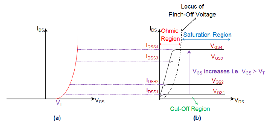
Cut-off region is a region in which the MOSFET will be OFF as there will be no current flow through it. In this region, MOSFET behaves like an open switch and is thus used when they are required to function as electronic switches.
Ohmic or linear region is a region where in the current IDS increases with an increase in the value of VDS. When MOSFETs are made to operate in this region, they can be used as amplifiers.
In saturation region, the MOSFETs have their IDS constant inspite of an increase in VDS and occurs once VDS exceeds the value of pinch-off voltage VP. Under this condition, the device will act like a closed switch through which a saturated value of IDS flows. As a result, this operating region is chosen whenever MOSFETs are required to perform switching operations.
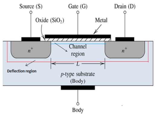
Fig: (a) Transfer Characteristics (b) Output Characteristics of NMOS
NMOS
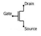
NMOS is built on a p-type substrate with n-type source and drain diffused on it. Here, the majority carriers are electrons. When a high voltage is applied to the gate, the NMOS conducts and when low voltage is applied to the gate, it does not conduct. NMOS is faster than PMOS, as the carriers are electrons that travel twice as fast as the holes.
PMOS
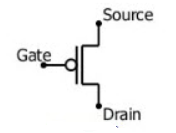
P-MOS consists of P-type Source and Drain diffused on an N-type substrate. Here, majority carriers are holes. When a high voltage is applied to the gate, the PMOS does not conduct and when a low voltage is applied, it conducts. These devices are more immune to noise than NMOS devices.
CMOS Applications
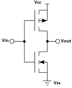
The inverter circuit as shown in the figure below. It consists of PMOS and NMOS FET. The input A serves as the gate voltage for both transistors.
The NMOS transistor has an input from Vss (ground) and PMOS transistor has an input from Vdd. The terminal Y is output. When a high voltage (~ Vdd) is given at input terminal (A) of the inverter, the PMOS becomes open circuit and NMOS switched OFF so the output will be pulled down to Vss.
When a low-level voltage (<Vdd, ~0v) applied to the inverter, the NMOS switched OFF and PMOS switched ON. So the output becomes Vdd or the circuit is pulled up to Vdd.
INPUT | LOGIC INPUT | OUTPUT | LOGIC OUTPUT |
0 V | 0 | Vdd | 1 |
Vdd | 1 | 0 v | 0 |
The VTC of complementary CMOS inverter is as shown in above Figure. The characteristics are divided into five regions of operations discussed as below :
Region A :
In this region the input voltage of inverter is in the range 0 Vin VTHn. Hence the NMOS is in cut-off and PMOS is in linear region and output voltage is VDD.
Region B :
In this region VTHn Vin < VDD2 in which p device is in linear region and n device is in saturation.
References:
1. Electronic Devices Circuit Theory - by Rober L. Boylestad 11th Edition, Pearson Publication, 2014
2. Microelectronic Circuits by A. S. Sedra and Kenneth C. Smith 7th Edition, Oxford University Press. 2017
3. Digital Design by M. Morris Mano, 5th Edition, Pearson Publication, 2016.