Unit - 4
Pulse modulation systems
In PAM, amplitude of pulses is varied in accordance with instantaneous value of modulating signal.
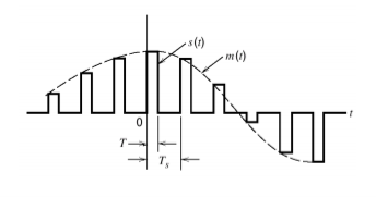
Fig 1 PAM waveform
PAM Generation:
The carrier which is in the form of narrow pulses has frequency fc. The uniform sampling takes place in multiplier to generate PAM signal. Samples are placed Ts sec away from each other.
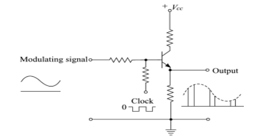
Fig 2 PAM Modulator
- The circuit is simple emitter follower.
- In the absence of the clock signal, the output follows input.
- The modulating signal is applied as the input signal.
- Another input to the base of the transistor is the clock signal.
- The frequency of the clock signal is made equal to the desired carrier pulse train frequency.
- The amplitude of the clock signal is chosen the high level is at ground level(0v)
- Low level at some negative voltage sufficient to bring the transistor in cut-off region.
- When clock is high, circuit operates as emitter follower and the output follows in the input modulating signal.
- When clock signal is low, transistor is cut-off and output is zero.
- Thus, the output is the desired PAM signal.
PAM Demodulator:
The PAM demodulator circuit which is just an envelope detector followed by a second order op-amp low pass filter (to have good filtering characteristics) is as shown below

Fig 3 PAM Demodulator
Key takeaway
The carrier which is in the form of narrow pulses has frequency fc. The uniform sampling takes place in multiplier to generate PAM signal. Samples are placed Ts sec away from each other.
There are two types of PTM systems. They are Pulse width modulation (PWM) and Pulse Position Modulation (PPM).
Pulse Width Modulation
In this type of modulation, the amplitude is maintained constant but the width of each pulse is varied in accordance with instantaneous value of the analog signal. In PWM information is contained in width variation. This is similar to FM. In pulse width modulation (PWM), the width of each pulse is made directly proportional to the amplitude of the information signal.
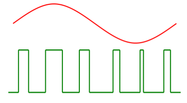
Fig 4 PWM waveform
PPM
In this type of modulation, the sampled waveform has fixed amplitude and width whereas the position of each pulse is varied as per instantaneous value of the analog signal. PPM signal is further modification of a PWM signal.
PPM and PWM modulator
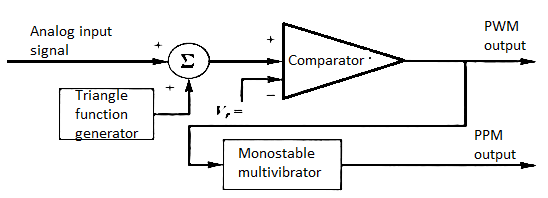
Fig 4 PTM Modulator
- The PPM signal can be generated from PWM signal.
- The PWM pulses obtained at the comparator output are applied to a mono stable multi vibrator which is negative edge triggered.
- Hence for each trailing edge of PWM signal, the monostable output goes high. It remains high for a fixed time decided by its RC components.
- Thus, as the trailing edges of the PWM signal keeps shifting in proportion with the modulating signal, the PPM pulses also keep shifting.
- Therefore, all the PPM pulses have the same amplitude and width. The information is conveyed via changing position of pulses.
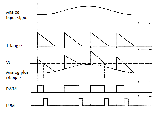
Fig 5 PWM and PPM Modulation waveforms.
PWM Demodulator
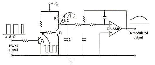
Fig 6 PWM Demodulator
- Transistor T1 works as an inverter.
- During time interval A-B when the PWM signal is high the input to transistor T2 is low.
- Therefore, during this time interval T2 is cut-off and capacitor C is charged through an R-C combination.
- During time interval B-C when PWM signal is low, the input to transistor T2 is high, and it gets saturated.
- The capacitor C discharges rapidly through T2.
- The collector voltage of T2 during BC is low.
- Thus, the waveform at the collector of T2is similar to saw-tooth waveform whose envelope is the modulating signal.
- Passing it through 2nd order op-amp Low Pass Filter, gives demodulated signal.
PPM Demodulator
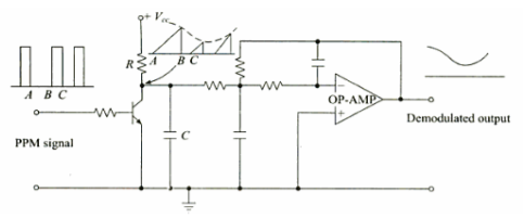
Fig 7 PPM Demodulator
- The gaps between the pulses of a PPM signal contain the information regarding the modulating signal.
- During gap A-B between the pulses the transistor is cut-off and the capacitor C gets charged through R-C combination.
- During the pulse duration B-C the capacitor discharges through transistor and the collector voltage becomes low.
- Thus, waveform across collector is saw-tooth waveform whose envelope is the modulating signal.
- Passing it through 2nd order op-amp Low Pass Filter, gives demodulated signal.
Key takeaway
In pulse time modulation system, we use the increased bandwidth consumed by pulses to obtain an improvement in noise performance by representing the sample values of the message signal by some property of pulse rather than amplitude.
Comparison between PAM, PPM and PWM
SR. NO. | PARAMETER | PAM | PWM | PPM |
1 | Type of Carrier | Train of Pulses | Train of Pulses | Train of Pulses |
2 | Variable Characteristic of the Pulsed Carrier | Amplitude | Width | Position |
3 | Bandwidth Requirement | Low | High | High |
4 | Noise Immunity | Low | High | High |
5 | Information Contained in | Amplitude Variations | Width Variations | Position Variations |
6 | Transmitted Power | Varies with amplitude of pulses | Varies with variation in width | Remains Constant |
7 | Need to transmit synchronizing pulses | Not needed | Not needed | Necessary |
8 | Complexity of generation and detection | Complex | Easy | Complex |
9 | Similarity with other Modulation Systems | Similar to AM | Similar to FM | Similar to PM |
10 | Output waveforms | Refer Figure down | Refer Figure down | Refer Figure down |
Basic Elements of PCM
The transmitter section comprises of Sampling, Quantizing and Encoding. The low pass filter prior to sampling prevents aliasing of the message signal.
The basic operations in the receiver section are regeneration of impaired signals, decoding, and reconstruction of the quantized pulse train.
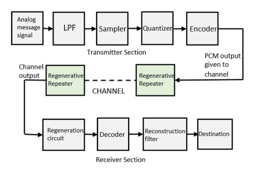
Fig.8: PCM
Low Pass Filter
This filter eliminates the high frequency components present in the input analog signal to avoid aliasing of the message signal.
Sampler
It helps to collect the sample data at instantaneous values of message signal, so as to reconstruct the original signal. The sampling rate must be in accordance with the sampling theorem.
Quantizer
It reduces excessive bits and confines the data. It reduces the redundant bits and compresses the value of the sampled output.
Encoder
The digitization of analog signal is done by the encoder. It designates each quantized level by a binary code. Encoding minimizes the bandwidth used.
Regenerative Repeater
It increases the signal strength. The output of the channel also has one regenerative repeater circuit, to compensate the signal loss and reconstruct the signal, and also to increase its strength.
Decoder
The decoder circuit decodes the pulse coded waveform to reproduce the original signal. This circuit acts as the demodulator.
Reconstruction Filter
After the digital-to-analog conversion is done by the regenerative circuit and the decoder, a low-pass filter is employed, called as the reconstruction filter to get back the original signal.
Hence, the Pulse Code Modulator circuit digitizes the given analog signal, codes it and samples it, and then transmits it in an analog form. This whole process is repeated in a reverse pattern to obtain the original signal.
Key takeaway
The transmitter section comprises of Sampling, Quantizing and Encoding. The low pass filter prior to sampling prevents aliasing of the message signal.
The basic operations in the receiver section are regeneration of impaired signals, decoding, and reconstruction of the quantized pulse train.
This is a form of distortion of a signal, in which one or more symbols interfere with subsequent signals, causing noise or delivering a poor output.
Causes of ISI
The main causes of ISI are −
- Multi-path Propagation
- Non-linear frequency in channels
The ISI is unwanted and should be completely eliminated to get a clean output. The causes of ISI should also be resolved in order to lessen its effect.
To view ISI in a mathematical form present in the receiver output, we can consider the receiver output.
The receiving filter output y(t)y(t) is sampled at time ti=iTb (with i taking on integer values), yielding –
y(ti)= μ∑akp(iTb−kTb)
= μai+μ∑akp(iTb−kTb)
In the above equation, the first term μai is produced by the ith transmitted bit.
The second term represents the residual effect of all other transmitted bits on the decoding of the ith bit. This residual effect is called as Inter Symbol Interference.
In the absence of ISI, the output will be −
y(ti)=μai
This equation shows that the ith bit transmitted is correctly reproduced. However, the presence of ISI introduces bit errors and distortions in the output.
While designing the transmitter or a receiver, it is important that you minimize the effects of ISI, so as to receive the output with the least possible error rate.
Key takeaway
The main causes of ISI are −
- Multi-path Propagation
- Non-linear frequency in channels
An eye diagram or eye pattern is simply a graphical display of a serial data signal with respect to time that shows a pattern that resembles an eye.
The signal at the receiving end of the serial link is connected to an oscilloscope and the sweep rate is set so that one- or two-bit time periods (unit intervals or UI) are displayed. This causes bit periods to overlap and the eye pattern to form around the upper and lower signal levels and the rise and fall times. The eye pattern readily shows the rise and fall time lengthening and rounding as well as the horizontal jitter variation.
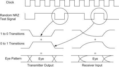
Fig. 9: eye diagram
For reliable communication, we need to have a quality output. The transmission losses of the channel and other factors affecting the quality of the signal. The most occurring loss, as we have discussed, is the ISI.
To make the signal free from ISI, and to ensure a maximum signal to noise ratio, we need to implement a method called Equalization.

Fig.10: Equalization
The noise and interferences which are denoted in the figure, are likely to occur, during transmission. The regenerative repeater has an equalizer circuit, which compensates the transmission losses by shaping the circuit. The Equalizer is feasible to get implemented.
Key takeaway
To make the signal free from ISI, and to ensure a maximum signal to noise ratio, we need to implement a method called Equalization.
There are two types of Quantization - Uniform Quantization and Non-uniform Quantization.
The type of quantization in which the quantization levels are uniformly spaced is termed as a Uniform Quantization. The type of quantization in which the quantization levels are unequal and mostly the relation between them is logarithmic, is termed as a Non-uniform Quantization.
Companding
It is a combination of Compressing and Expanding, which means that it does both. This is a non-linear technique used in PCM which compresses the data at the transmitter and expands the same data at the receiver. The effects of noise and crosstalk are reduced by using this technique.
There are two types of Companding techniques. They are −
A-law Companding Technique
- Uniform quantization is achieved at A = 1, where the characteristic curve is linear and no compression is done.
- A-law has mid-rise at the origin. Hence, it contains a non-zero value.
- A-law companding is used for PCM telephone systems.
µ-law Companding Technique
- Uniform quantization is achieved at µ = 0, where the characteristic curve is linear and no compression is done.
- µ-law has mid-tread at the origin. Hence, it contains a zero value.
- µ-law companding is used for speech and music signals.
µ-law is used in North America and Japan.
Key takeaway
A-law Companding Uniform quantization is achieved at A = 1, where the characteristic curve is linear and no compression is done.
In pulse modulation the time division multiplexing makes the maximum utilisation of the transmission channel. The TDM can be analog or digital. The digital multiplexing is discussed below. The block diagram for TDM is shown below. N PAM channels are multiplexed and each channel to be transmitted is passed through the LPF. The input to the commutators is the signal coming out from the LPF. The commutator rotates at the rate of fs. A t the receiver the demodulator separates the time multiplexed input channels. These signal pass through the low-pass reconstruction filters. If W is the highest signal frequency, then according to the sampling theorem
fs 2W
2W
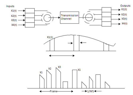
Fig 11 TDM system block diagram and waveform [Ref 6]
The time space between two samples is given by
Ts = 1/fs
Ts 2W
2W
If there are N input channels then the space between two samples is given by
Space between two samples = Ts/N
The number of pulses/sec are called as signalling rate of TDM denoted by r
r= Nfs
For PAM/TDM Signalling rate r  2NW
2NW
Synchronisation in TDM
There should always be synchronisation in transmitter and receiver. Usually, markers are inserted to indicate the separation between the frames. Synchronisation is obtained due to these marker pulses but the number of channels to be multiplexed is reduced by one. They become N-1.
Crosstalk
In TDM transmission the signal is converted to smooth modulating waveform when passed through the baseband filter. The baseband value passes through the values of all the individual samples.
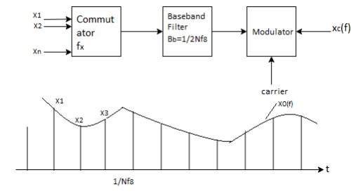
Fig 12 TDM transmission with baseband filtering and its waveform
Due to this baseband filter crosstalk arises in between two samples. This interference can be reduced by increasing the distance between individual signal samples. The minimum distance required to avoid crosstalk between two samples is called as guard time.
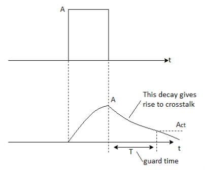
Fig 13 Applied rectangular pulse and its response
From above figure we see that even after the pulse is removed the response decays from its value A and then takes longer period. The guard time Tg represents minimum pulse spacing. After guard time end the pulse tail is less than Act.
Act = A
B= Bandwidth of signal
Key takeaway
The time space between two samples is given by
Ts = 1/fs
Ts 2W
2W
The number of pulses/sec are called as signalling rate of TDM denoted by r
r= Nfs
For PAM/TDM Signalling rate r  2NW
2NW
Example
Twelve different message signals each of bandwidth 20kHz are to be multiplexed and transmitted. Determine the minimum bandwidth required for PAM/TDM system?
Sol: No. Of channels N =12
Bandwidth of each channel fm = 20kHz
Minimum bandwidth required to avoid crosstalk is = Nfm = 20 x 12 = 240kHz
A line code is the code used for data transmission of a digital signal over a transmission line. This process of coding is chosen so as to avoid overlap and distortion of signal such as inter-symbol interference.
Properties of Line Coding
Following are the properties of line coding −
- As the coding is done to make more bits transmit on a single signal, the bandwidth used is much reduced.
- For a given bandwidth, the power is efficiently used.
- The probability of error is much reduced.
- Error detection is done and the bipolar too has a correction capability.
- Power density is much favorable.
- The timing content is adequate.
- Long strings of 1s and 0s is avoided to maintain transparency.
Types of Line Coding
There are 3 types of Line Coding
- Unipolar
- Polar
- Bi-polar
Unipolar Signaling
Unipolar signaling is also called as On-Off Keying or simply OOK.
The presence of pulse represents a 1 and the absence of pulse represents a 0.
There are two variations in Unipolar signaling −
- Non-Return to Zero NRZ
- Return to Zero RZRZ
Unipolar Non-Return to Zero NRZ
In this type of unipolar signaling, a High in data is represented by a positive pulse called as Mark, which has a duration T0 equal to the symbol bit duration. A Low in data input has no pulse.
The following figure clearly depicts this.
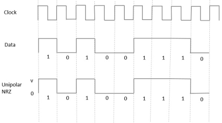
Fig 14 Uni-polar NRZ
Advantages
The advantages of Unipolar NRZ are −
- It is simple.
- A lesser bandwidth is required.
Disadvantages
The disadvantages of Unipolar NRZ are −
- No error correction done.
- Presence of low frequency components may cause the signal droop.
- No clock is present.
- Loss of synchronization is likely to occur (especially for long strings of 1s and 0s).
Unipolar Return to Zero RZRZ
In this type of unipolar signaling, a High in data, though represented by a Mark pulse, its duration T0 is less than the symbol bit duration. Half of the bit duration remains high but it immediately returns to zero and shows the absence of pulse during the remaining half of the bit duration.
It is clearly understood with the help of the following figure.
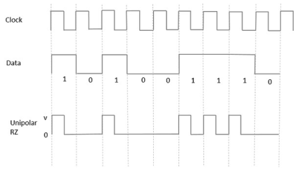
Fig 15 Unipolar RZ
Advantages
The advantages of Unipolar RZ are −
- It is simple.
- The spectral line present at the symbol rate can be used as a clock.
Disadvantages
The disadvantages of Unipolar RZ are −
- No error correction.
- Occupies twice the bandwidth as unipolar NRZ.
- The signal droop is caused at the places where signal is non-zero at 0 Hz.
Polar Signaling
There are two methods of Polar Signaling. They are −
- Polar NRZ
- Polar RZ
Polar NRZ
In this type of Polar signaling, a High in data is represented by a positive pulse, while a Low in data is represented by a negative pulse. The following figure depicts this well.
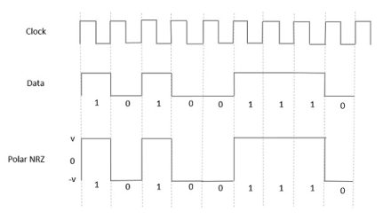
Fig 16 Polar NRZ
Advantages
The advantages of Polar NRZ are −
- It is simple.
- No low-frequency components are present.
Disadvantages
The disadvantages of Polar NRZ are −
- No error correction.
- No clock is present.
- The signal droop is caused at the places where the signal is non-zero at 0 Hz.
Polar RZ
In this type of Polar signaling, a High in data, though represented by a Mark pulse, its duration T0 is less than the symbol bit duration. Half of the bit duration remains high but it immediately returns to zero and shows the absence of pulse during the remaining half of the bit duration.
However, for a Low input, a negative pulse represents the data, and the zero level remains same for the other half of the bit duration. The following figure depicts this clearly.
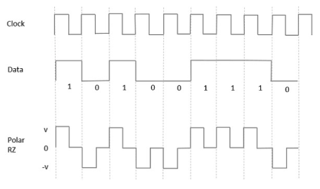
Fig 17 Polar RZ
Advantages
The advantages of Polar RZ are −
- It is simple.
- No low-frequency components are present.
Disadvantages
The disadvantages of Polar RZ are −
- No error correction.
- No clock is present.
- Occupies twice the bandwidth of Polar NRZ.
- The signal droop is caused at places where the signal is non-zero at 0 Hz.
Bipolar Signaling
This is an encoding technique which has three voltage levels namely +, - and 0. Such a signal is called as duo-binary signal.
An example of this type is Alternate Mark Inversion AMIAMI. For a 1, the voltage level gets a transition from + to – or from – to +, having alternate 1s to be of equal polarity. A 0 will have a zero-voltage level.
Even in this method, we have two types.
- Bipolar NRZ
- Bipolar RZ
From the models so far discussed, we have learnt the difference between NRZ and RZ. It just goes in the same way here too. The following figure clearly depicts this.
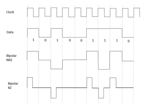
Fig 18 Bipolar RZ and Bipolar NRZ
The above figure has both the Bipolar NRZ and RZ waveforms. The pulse duration and symbol bit duration are equal in NRZ type, while the pulse duration is half of the symbol bit duration in RZ type.
Advantages
Following are the advantages −
- It is simple.
- No low-frequency components are present.
- Occupies low bandwidth than unipolar and polar NRZ schemes.
- This technique is suitable for transmission over AC coupled lines, as signal drooping doesn’t occur here.
- A single error detection capability is present in this.
Disadvantages
Following are the disadvantages −
- No clock is present.
- Long strings of data causes loss of synchronization.
Power Spectral Density
The function which describes how the power of a signal got distributed at various frequencies, in the frequency domain is called as Power Spectral Density PSD.
PSD is the Fourier Transform of Auto-Correlation Similarity between observations. It is in the form of a rectangular pulse.
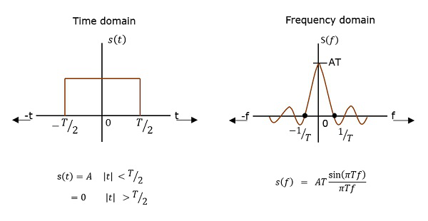
Fig 19 PSD
Key Takeaways:
- Line coding determines how the binary data is represented on the link.
- The mark density (MD) of a binary data pattern is defined as the number of one bit in the pattern, divided by the length of the pattern:

Assume that there are n channels each channel is bandlimited to fm to be time division multiplexed. Let N be the length of the PCM code so that there are 2N = L quantisation levels. Then the bit rate of the PCM system becomes
Bit rate = 2fm [n(N+1) + 1] Hz
If N>>1 and n>>1 for practical situations, the bit rate is given by
Bit rate = 2nNfm
Then bandwidth of PCM is given by
BW = Bit rate/2
Signal to noise ratio in PCM:
SNR= (signal power)/ (noise power)
Signal power=p Quantization error=ἐ=xq(nT)-x(nT) =(xmax-xmin)/2n
Where, n is code word length.
|e| =
Quantization noise power=E[e2]
 (limits from - to )
 (limits from - to )


If the signal is defined from –xmax to +xmax
Then Δ =(2xmax)/2n
(S/N) PCM=(12p)/(2xmax/2n)2
=(12p*22n)/(4xmax2)
=(3p*22n)/xmax2
For normalized signal xmax=1
Then SNR for normalized signal is slightly less than or equal to 3.1*22n i.e.
(S/N) PCM for normalized signal≤3.1*22n
(S/N) PCM in dB=10log10(3*22n) =4.8+6n
For increasing one bit then (S/N) PCB will increase to 6dB.
Key takeaway
(S/N) PCM for normalized signal≤3.1*22n
(S/N) PCM in dB=10log10(3*22n) =4.8+6n
Examples
Q1) A PCM system uses a uniform quantizer followed by a 7-bit encoder. The system bit rate is 50Mbits/sec. Calculate the maximum BW of the message signal for which this system operates?
A1) Bit rate r = 50Mbits/sec
N=7
Bit rate r=Nfs
fs=50Mbits/sec/7=7.14MHz
Maximum signal BW =fs/2 = 7.14/2= 3.57MHz
Q2) The BW of a video signal is 4.5MHz. The signal is to be transmitted using PCM with the number of quantization level Q = 1024. The sampling rate should be 20% higher than the Nyquist rate. Calculate the system bit rate?
A2) Band width W =4.5MHz
From Nyquist rate fs= 2W= 9MHz
But fs should be 20% higher than Nyquist rate
fs = 1.2 x 9MHz = 10.8MHz
Q=2N
1024=2N
N =10
System bit rate r= Nfs = 10x10.8MHz = 108MHz
Q3) A band-limited signal m(t) of 3 kHz bandwidth is sampled at rate of 33⅓ % higher than the Nyquist rate. The maximum allowable error in the sample amplitude (i.e., the maximum quantization error) is 0.5% of the peak amplitude mp. Assume binary encoding. Find the minimum bandwidth of the channel to transmit the encoded binary signal.
A3) The Nyquist rate is RN = 2 x 3000 Hz = 6000 Hz (samples/second), but the actual rate is 33⅓ % higher, so that is 6000 Hz + (⅓ x 6000) = 8000 Hz.
The quantization step is and the maximum quantization error is plus/minus /2. Hence, we can write
/2 =mp/L=0.5mp/100
L= 200
For binary coding, L, must be a power of two; therefore, knowing that L = 27 = 128 and 28 = 256, we must choose n = 8 to guarantee better than a 0.5% error.
Having chosen n = 8 to guarantee 0.5% error, to find the bandwidth required we note that Total number of bits per second = 8 bits 8000 Hz = 64,000 bits/second C However, we know we can transmit 2 bits/Hz of bandwidth, so it requires a bandwidth BT of
BT= C/2 =32000Hz or 32kHz
If 24 such signals are multiplexed on a single line (known as a T1 Line in the Telephone system, then CT1 = 24 x 64 kb/s = 1.536 Mb/s, and the bandwidth is 768 KHz.
Q4) We are given a signal m(t) = 2cos (2250 t) as the signal input. Find the SNR with 8-bit PCM.
A4) For 8-bit encoding, L = 2n where n = 8, therefore, the number of levels = 256.
The amplitude Am of the sinusoidal waveform means that mp = 2 volts.
The total signal swing possible (- mp to + mp) will be 2mp = 4 volts, therefore, the average signal power is Pave = [(Am )2 /2] = [22/2] = 2 watts.
The interval = [2mp /L] = 4 volts/256 levels = 1.625 10-2 volt
Using for the quantization noise Nq = [()2 /12], and taking Pave = 2 W, the SNR is given by


Q5) We are given a signal m(t) = 2cos(2250 t) as the signal input. If the minimum SNR is to be at least 36 dB, how many bits n are needed to encode the signal (i.e., find n)? Use signal power as mentioned in Q4.
A5) Note that 36 dB is numerically equivalent to 3,981 [about 4,000].
Remembering that the interval is = [2mp /L] and
2mp = 4 volts.

Therefore, we can determine the number of levels L, and then n.

The lowest integer number of bits n that will give at least 31.5 levels is n = 5 because 25 = 32 levels.
So, the answer is 5 bits.
Q6) The number of bits in a binary PCM system is increased from n to n+1. As a result, the signal quantization noise ratio will improve by a factor
(a) (n+ 1)/n
(b) 2(n+1) /n
(c) 4
(d)Which is independent of n.
A6)

For 


Q7) The bandwidth required for the transmission of a PCM signal increases by a factor of _____when the number of quantization levels is increased from 4 to 64.
(a) 2 Times (b) 3 Times (c) 4 Times (d)Which is independent of quantization levels
A7)
(Bandwidth)PCM=nfm
Where n-number of bits n in PCM code fm – signal bandwidth


Q8) A sinusoidal signal with peak-to-peak amplitude of 1.536 V is quantized into 128 levels using a midtread uniform quantizer. The quantization noise power is (a) 0.768 V (b)48 × 10-6 v2 (c) 12 × 10-6 v2 (d)3.072 V
A8)


Q9) In a PCM system, the signal m(t) = {sin (100πt) + cos(100πt)} V is sampled at the Nyquist rate. The samples are processed by a uniform quantizer with step size 0.75 V. The minimum data rate of the PCM system in bits per second is?
A9) Nyquist rate =2x50=100 samples/s
Step size = m(t)max - m(t)min/L
Number of levels L = √2-(-√2)/0.75 = 4
Number of bits required to encode 4 levels = 2bits/level
Data rate = 2x100=200 bits/s
Q10) A television signal with a bandwidth of 4.2 Mz is transmitted using binary PCM. The number of quantization levels are 512. Calculate (a) code word length (b) Transmission bandwidth (c) Final bit rate (d) Output signal to quantization noise ratio
A10)
Signal Bandwidth =4.2 MHz, N=512
(a) n= codeword length 

(b) Bandwidth 
(c) Final bit rate 

Bit rate 

The type of modulation, where the sampling rate is much higher and in which the step size after quantization is of a smaller value Δ, such a modulation is termed as delta modulation.
Features
- The quality is moderate.
- The design of the modulator and the demodulator is simple.
- The stair-case approximation of output waveform.
- The step-size is very small, i.e., Δ delta.
- The bit rate can be decided by the user.
- This involves simpler implementation.
Delta Modulation is a simplified form of DPCM technique, also viewed as 1-bit DPCM scheme. As the sampling interval is reduced, the signal correlation will be higher.
Delta Modulator
The Delta Modulator comprises of a 1-bit quantizer and a delay circuit along with two summer circuits. Following is the block diagram of a delta modulator.
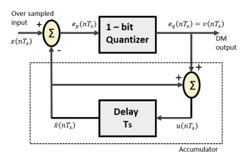
Fig.1: Delta Modulator
The predictor circuit in DPCM is replaced by a simple delay circuit in DM.
From the above diagram, we have the notations as −
- x(nTs)= over sampled input
- Ep(nTs) = summer output and quantizer input
- Eq(nTs) = quantizer output = v(nTs)
- xˆ(nTs) = output of delay circuit
- u(nTs) = input of delay circuit
Using these notations, now we shall try to figure out the process of delta modulation.
Ep(nTs)=x(nTs)−xˆ(nTs) ---------equation 1
=x(nTs)−u([n−1]Ts
=x(nTs)−[xˆ[[n−1]Ts]+v[[n−1]Ts]] -------equation 2
Further,
v(nTs)=eq(nTs)=S.sig.[ep(nTs)] ---------equation 3
u(nTs)=xˆ(nTs)+eq(nTs)
Where,
- xˆ(nTs) = the previous value of the delay circuit
- Eq(nTs) = quantizer output = v(nTs)
Hence,
u(nTs)=u([n−1]Ts)+v(nTs) ---------equation 4
Which means,
The present input of the delay unit
= The previous output of the delay unit + the present quantizer output the present quantizer output
Assuming zero condition of Accumulation,

Accumulated version of DM output =  --------equation 5
Now, note that
xˆ(nTs)=u([n−1]Ts)
= ---------equation 6
Delay unit output is an Accumulator output lagging by one sample.
From equations 5 & 6, we get a possible structure for the demodulator.
A Stair-case approximated waveform will be the output of the delta modulator with the step-size as delta (Δ). The output quality of the waveform is moderate.
Delta Demodulator
The delta demodulator comprises of a low pass filter, a summer, and a delay circuit. The predictor circuit is eliminated here and hence no assumed input is given to the demodulator.
Following is the diagram for delta demodulator.
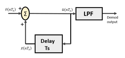
Fig.2 Delta Demodulator
From the above diagram, we have the notations as −
- vˆ(nTs) is the input sample
- uˆ(nTs) is the summer output
- x¯(nTs) is the delayed output
A binary sequence will be given as an input to the demodulator. The stair-case approximated output is given to the LPF.
Low pass filter is used for many reasons, but the prominent reason is noise elimination for out-of-band signals. The step-size error that may occur at the transmitter is called granular noise, which is eliminated here. If there is no noise present, then the modulator output equals the demodulator input.
Advantages of DM Over DPCM
- 1-bit quantizer
- Very easy design of the modulator and the demodulator
Key takeaway
The type of modulation, where the sampling rate is much higher and in which the step size after quantization is of a smaller value Δ, such a modulation is termed as delta modulation.
Delta modulation is subject to rate of rise over load problems whenever the input changes too rapidly for the stepped wave form to follow it. If the input signal level remains constant, the reconstructed Delta modulation waveform exhibits a hunting behaviour known as idling noise. This idling noise is a square wave at one half the clock rate. If the clock rate is much greater than twice the highest frequency in the input signal, most of the idling noise can be filtered out at the receiver.
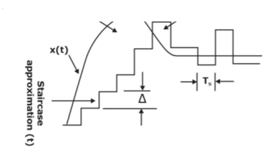
Fig 3 Slope Overload
Slope Overload: Slope overload distortion occurs when the analog input signal changes at a faster rate than the DAC can maintain it, the slope of the analog signal is greater than the delta modulator can maintain. In general, when the slope of stair case is less than (or) equal to modulating signal, the slope overloading occurs. Increasing the clock frequency reduces the probability of slope overload occurring. General method to reduce the slope overload is to increase the magnitude of the size. Assume the input for Delta modulation be f(t) = A cos ωmt.

If the step size used in the Delta modulation system is ‘Δ’, then the maximum (rate of rise) slope over load is / Ts


Granular noise: In general, Granular noise occurs
- When the original analog input signal has a relatively constant amplitude, the reconstructed signal has variations that were not present in the original signal. This is called granular noise
- The granular noise is analogous to the quantization noise in a PCM system.
- When the step size Δ is too large relative to the local slope characteristics of the input waveform x(t), thereby causing the stair case approximation u(t) to hunt around a relatively flat segment of the input waveform Granular noise can be reduced by decreasing the step size so that the stair case approximation may become more closer to the modulating signal.
There is a need to have a large step size to accommodate a wide dynamic range, whereas small step size is required for the accurate representation of relatively low-level signals.


Therefore, a granular noise can be removed by taking a small resolution of step size and a slope over load distortion can be removed by taking a large resolution.
Key takeaway
The input for Delta modulation be f(t) = A cos ωmt.

In digital modulation, we have come across certain problem of determining the step-size, which influences the quality of the output wave.
A larger step-size is needed in the steep slope of modulating signal and a smaller step size is needed where the message has a small slope. The minute details get missed in the process. So, it would be better if we can control the adjustment of step-size, according to our requirement in order to obtain the sampling in a desired fashion. This is the concept of Adaptive Delta Modulation.
Following is the block diagram of Adaptive delta modulator.
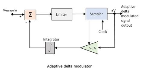
Fig. 4 Adaptive delta modulator
The gain of the voltage-controlled amplifier is adjusted by the output signal from the sampler. The amplifier gain determines the step-size and both are proportional.
ADM quantizes the difference between the value of the current sample and the predicted value of the next sample. It uses a variable step height to predict the next values, for the faithful reproduction of the fast-varying values.
Key takeaway
ADM quantizes the difference between the value of the current sample and the predicted value of the next sample. It uses a variable step height to predict the next values
Signal to Noise Ratio of Delta modulation system: It is the ratio of Signal power to the noise power Signal power=p
Quantization noise power=E[e2]
 (limits from - to )
 (limits from - to )


Signal power p= V2/2
Amplitude = Am
V=Am/√2
Signal Power = p = Am2/2R
Normalised Signal Power R=1, then P= Am2/2
To avoid the slope overload error in the delta modulation, the amplitude Am≤ 
By substituting, the normalised power signal power

Then the signal to noise ratio

S.No | Parameter of comparison | Pulse Code Modulation (PCM) | Delta Modulation(DM) | Adaptive Delta Modulation(ADM) | Differential code pulse modulation(DPCM) |
1. | Number of bits | It can use 4,8, or 16 bits per sample | It uses only one bit for one sample | It uses only one bit for one sample | Bits can be more than one but are less than PCM |
2. | Levels and step size | The number of levels depends on number of bits Level size is fixed. | Step size is kept fixed and cannot be varied. | According to the signal variation, step size varies. | Number of levels is fixed. |
3. | Quantization error and distortion | Quantization error depends on number of levels used. | Slope overload distortion and granular noise are present. | Quantization noise is present but other errors are absent. | Slope overload distortion and quantization noise is present. |
4. | Transmission bandwidth | Highest bandwidth is required since numbers of bits are high. | Lowest bandwidth is required. | Lowest bandwidth is required. | Bandwidth required is less than PCM. |
5. | Feedback | There is no feedback in transmitter or received | Feedback exists in transmitter. | Feedback exists. | Feedback exists. |
6. | Complexity of implementation | System is complex | Simple | Simple | Simple |
Differential pulse code modulation (DPCM) is a procedure of converting an analog into a digital signal in which an analog signal is sampled and then the difference between the actual sample value and its predicted value (predicted value is based on previous sample or samples) is quantized and then encoded forming a digital value.
DPCM code words represent differences between samples unlike PCM where code words represented a sample value.
Basic concept of DPCM - coding a difference, is based on the fact that most source signals show significant correlation between successive samples so encoding uses redundancy in sample values which implies lower bit rate.
Realization of basic concept (described above) is based on a technique in which we have to predict current sample value based upon previous samples (or sample) and we have to encode the difference between actual value of sample and predicted value (the difference between samples can be interpreted as prediction error).
Because it's necessary to predict sample value DPCM is form of predictive coding.
DPCM compression depends on the prediction technique, well-conducted prediction techniques lead to good compression rates, in other cases DPCM could mean expansion comparing to regular PCM encoding.

Fig.5: DPCM
Key Takeaways:
- DPCM code words represent differences between samples unlike PCM where code words represented a sample value.
- Basic concept of DPCM - coding a difference, is based on the fact that most source signals show significant correlation between successive samples so encoding uses redundancy in sample values which implies lower bit rate.
Examples
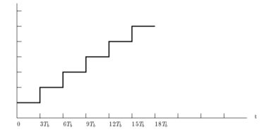
Q1) Figure shows a PCM wave in which the amplitude levels of +1 volt and -1 volts are used to represent binary symbols 1 and 0 respectively. The codeword used consists of three bits. Find the sampled version of an analog signal from which this PCM is derived.
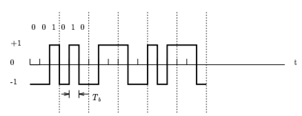
A1) The sample analog signal has the following waveform
Q2) Show that the use of A-law companding provides a ratio of maximum step size to minimum step size equal to the parameter A.
A2)
For the A-law companding we have,

For small input x, the A-law is characterized by its derivatives

For large input, on the other hand, it is characterized by

Accordingly
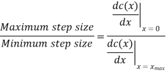
Q3) Consider a DPCM system whose transmitter uses a first order predictor optimized in the minimum mean squared sense. Calculate the prediction gain of the system for the following values of the correlation coefficient for the
(i) 

The correlation coefficient  equals the autocorrelation function of the message signal for the delay T, normalized with respect to the mean square value of the signal.
(b) Suppose that the predictor is made suboptimal by setting the coefficient  Calculate the resulting values of the prediction gain for the two values of
  specified in part(a). What is the minimum value of
  for which the suboptimum system produces a prediction gain greater than one?
A3)
(a) The prediction Gain is

As shown in the class, the prediction error variance 
(i) 

(ii) 

(ii) The prediction error is

Correspondingly, the prediction error variance is

Substituting (1) in (2), and simplifying we get

The prediction error variance is
The prediction gain is therefore

(i) 

(ii) 

The minimum value for which the prediction gain in (3) exceeds unity is when the correlation coefficient  is less than 0.5
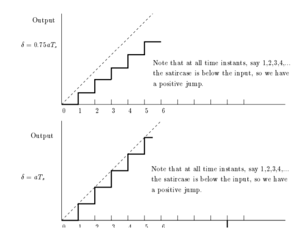
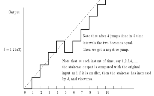
Q4) The ramp signal x(t)=a(t) is applied to a delta modulator that operates with a sampling period  and step size =2δ
(a) Show slope-overload distortion occurs is δ<
(b) Sketch the modulator output of the following three values of the step size
(i)  (ii)
(ii)  (iii)
(iii) 
A4)
(a) In a period  the input signal rises by
  i.e.,
i.e.,  , whereas the output of the delta modulator rises by an amount equal to δ. Hence, slope overload distortion occurs if
(b) For each of the three values of δ, the modulator output is as shown in Fig.
This figure illustrates that slope overload distortion occurs if
Figure is shown in next question.
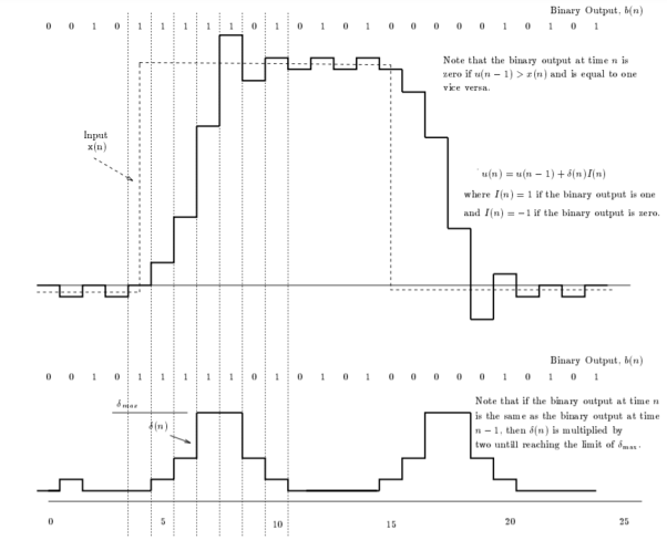
Q5) Consider an adaptive delta modulator, for which the input signal  is given by

The adaption algorithm for the modulator is defined with the constant K equal to 2. The maximum and minimum permissible values of the step size are as follows:


The initial conditions are given by


Plot the stair case approximation  and the binary output for
A5)
Let the sampling period  . Then

The binary output, b(n), is equal to zero if e(n)<0 and is equal to one, otherwise.

This means that I(n) is one if the binary output is one and is -1 if the binary output is zero.


For the reconstruction, we have,

Resulting in,

Initial conditions:


Using these initial conditions and inputs defining relations for the adaptive delta modulation, we get the approximation u(n), the adaptive variation of δ(n), and the resulting binary output b(n) as shown in fig.
Q6) A Delta modulated system is designed to operate at five times the Nyquist Rate. The signal bandwidth B at its input port is 3 kHz and the quantized step is 250 millivolts (0.25 volt). For this problem we assume a 2 kHz sinusoidal input – Find the maximum amplitude Am of this 2 kHz tone.
A6) We know that B = 3 kHz, fm = 2 kHz and = 250 mV.
The Nyquist rate is 3,000 2 = 6,000 Hz. So, five time the Nyquist rate is 30,000 Hz = fs.
Using the relationship

Q7) A one kilohertz (1 kHz) signal m(t) is sampled at 8 kHz with 12-bit encoding for PCM transmission.
(a) How many bits are transmitted per second in in PCM? What is the bandwidth required in this case?
(b) Now switch to using DM with 8 kHz sampling. How many bits are transmitted per second using DM? What is the bandwidth required in using DM?
A7) We know that the signal frequency is fm = 1 kHz and the sampling rate is 8 kHz.
(a) For PCM we have 8,000 samples per second and 12 bits per sample; which equals 96,000 bits/second. The bandwidth is one-half of this giving 48,000 Hz.
(b) Now for DM we have 1 bit per sample at 8,000 samples per second. Thus, we have 8,000 bits per second and a bandwidth of 4,000 Hz.
The word binary represents two bits. M represents a digit that corresponds to the number of conditions, levels, or combinations possible for a given number of binary variables.
This is the type of digital modulation technique used for data transmission in which instead of one bit, two or more bits are transmitted at a time. As a single signal is used for multiple bit transmission, the channel bandwidth is reduced.
M-ary Equation
If a digital signal is given under four conditions, such as voltage levels, frequencies, phases, and amplitude, then M = 4.
The number of bits necessary to produce a given number of conditions is expressed mathematically as
N=log2M
Where
N is the number of bits necessary
M is the number of conditions, levels, or combinations possible with N bits.
The above equation can be re-arranged as
2N=M
For example, with two bits, 22 = 4 conditions are possible.
M-ary PSK
This is called as M-ary Phase Shift Keying M−ary PSK
The phase of the carrier signal, takes on M different levels.
Representation of M-ary PSK
Si(t)=√2E/T cos(wot+ϕit) 0≤t≤T and i=1,2...M
ϕi(t)=2πiM where i=1,2,3......M
Some prominent features of M-ary PSK are −
- The envelope is constant with more phase possibilities.
- This method was used during the early days of space communication.
- Better performance than ASK and FSK.
- Minimal phase estimation error at the receiver.
- The bandwidth efficiency of M-ary PSK decreases and the power efficiency increases with the increase in M.
So far, we have discussed different modulation techniques. The output of all these techniques is a binary sequence, represented as 1s and 0s
M-ary FSK
This is called as M-ary Frequency Shift Keying M−aryFSK.
The frequency of the carrier signal, takes on M different levels.
Representation of M-ary FSK


Key takeaway
The transmitted M number of signals are equal in energy and duration.
The signals are separated by 1/2Ts Hz making the signals orthogonal to each other.
Since M signals are orthogonal, there is no crowding in the signal space.
The bandwidth efficiency of M-ary FSK decreases and the power efficiency increases with the increase in M.
References:
[1] John G.Proakis, M. Salehi, Communication Systems Engineering, 2nd ed. New
Delhi, India. PHI Learning Private Limited, 2009.
[2] R.P Singh and S.D Sapre, Communication Systems Analog & Digital, 2nd ed. New Delhi, India. Tata McGraw Hill Education Private Limited, 2009.