Unit -1
Fundamentals of Digital Systems and logic families
1) Basic gates
2) Universal gates
3) Special gates
AND gate
It is a digital circuit that consists of two or more inputs and a single output which is the logical AND of all those inputs. It is represented with the symbol ‘.’.
The following is the truth table of 2-input AND gate.
A | B | Y = A.B |
0 | 0 | 0 |
0 | 1 | 0 |
1 | 0 | 0 |
1 | 1 | 1 |
Here A, B are the inputs and Y is the output of two input AND gate.
If both inputs are ‘1’, then only the output, Y is ‘1’. For remaining combinations of inputs, the output, Y is ‘0’.
The figure below shows the symbol of an AND gate, which is having two inputs A, B and one output, Y.

Fig. : AND gate (ref. 1)
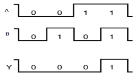
Timing Diagram:
OR gate
It is a digital circuit which has two or more inputs and a single output which is the logical OR of all those inputs. It is represented with the symbol ‘+’.
The truth table of 2-input OR gate is:
A | B | Y = A + B |
0 | 0 | 0 |
0 | 1 | 1 |
1 | 0 | 1 |
1 | 1 | 1 |
Here A, B are the inputs and Y is the output of two input OR gate.
When both inputs are ‘0’, then only the output, Y is ‘0’. For remaining combinations of inputs, the output, Y is ‘1’.
The figure below shows the symbol of an OR gate, which is having two inputs A, B and one output, Y.
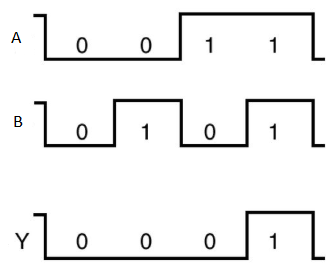
Fig. : OR gate (ref. 1)
Timing Diagram:

NOT gate
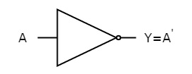
It is a digital circuit that has one input and one output. Here the output is the logical inversion of input. Hence, it is also called as an inverter.
The truth table of NOT gate is:
A | Y = A’ |
0 | 1 |
1 | 0 |
Here A and Y are the corresponding input and output of NOT gate. When A is ‘0’, then, Y is ‘1’. Similarly, when, A is ‘1’, then, Y is ‘0’.
The figure below shows the symbol of NOT gate, which has one input, A and one output, Y.
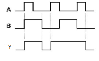
Fig. : NOT gate (ref. 1)
Timing Diagram:
Universal gates
NAND gate
It is a digital circuit which has two or more inputs and single output and it is the inversion of logical AND gate.
The truth table of 2-input NAND gate is:
A | B | Y = (A.B)’ |
0 | 0 | 1 |
0 | 1 | 1 |
1 | 0 | 1 |
1 | 1 | 0 |
Here A, B are the inputs and Y is the output of two input NAND gate. When both inputs are ‘1’, then the output, Y is ‘0’. If at least one of the input is zero, then the output, Y is ‘1’. This is just the inverse of AND operation.
The image shows the symbol of NAND gate:
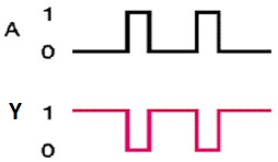
Fig.: NAND gate (ref. 1)
NAND gate works same as AND gate followed by an inverter.
Timing Diagram:

NOR gate
It is a digital circuit that has two or more inputs and a single output which is the inversion of logical OR of all inputs.
The truth table of 2-input NOR gate is:
A | B | Y = (A+B)’ |
0 | 0 | 1 |
0 | 1 | 0 |
1 | 0 | 0 |
1 | 1 | 0 |
Here A and B are the two inputs and Y is the output. If both inputs are ‘0’, then the output is ‘1’. If any one of the input is ‘1’, then the output is ‘0’. This is exactly opposite to two input OR gate operation.
The symbol of NOR gate is:
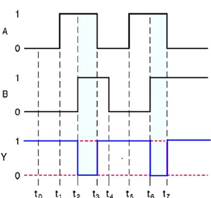
Fig.: NOR gate (ref. 1)
NOR gate works exactly same as that of OR gate followed by an inverter.
Timing Diagram:

Special Gates
Ex-OR gate
It stands for Exclusive-OR gate. Its function varies when the inputs have even number of ones.
The truth table of 2-input Ex-OR gate is:
A | B | Y = A⊕B |
0 | 0 | 0 |
0 | 1 | 1 |
1 | 0 | 1 |
1 | 1 | 0 |
Here A, B are the inputs and Y is the output of two input Ex-OR gate. The output (Y) is zero instead of one when both the inputs are one.
Therefore, the output of Ex-OR gate is ‘1’, when only one of the two inputs is ‘1’. And it is zero, when both inputs are same.
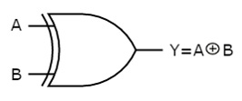
The symbol of Ex-OR gate is as follows:
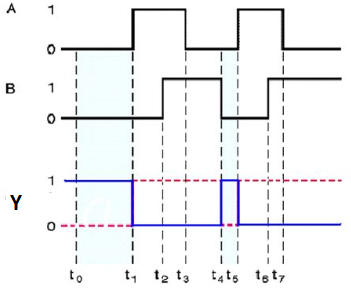
Fig.: XOR gate (ref. 1)
It is similar to that of OR gate with an exception for few combination(s) of inputs. Hence, the output is also known as an odd function.
Timing Diagram:
Ex-NOR gate
It stands for Exclusive-NOR gate. Its function is same as that of NOR gate except when the inputs having even number of ones.
The truth table of 2-input Ex-NOR gate is:
A | B | Y = A⊙B |
0 | 0 | 1 |
0 | 1 | 0 |
1 | 0 | 0 |
1 | 1 | 1 |
Here A, B are the inputs and Y is the output. It is same as Ex-NOR gate with the only modification in the fourth row. The output is 1 instead of 0, when both the inputs are one.
Hence the output of Ex-NOR gate is ‘1’, when both inputs are same and 0, when both the inputs are different.
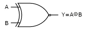
The symbol of Ex-NOR gate is:
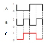
Fig.: XNOR gate (ref. 1)
It is similar to NOR gate except for few combination(s) of inputs. Here the output is ‘1’, when even number of 1 is present at the inputs. Hence is also called as an even function.
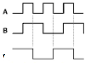
Timing Diagram:
Commutative Law
x + y = y + x
x.y = y.x
Associative Law
x + (y + z) = (x + y) + z
x.(y.z) = (x.y).z
Distributive Law
x.(y + z) = x.y + x.z
x + (y.z) = (x + y).(x + z)
A digital system understands positional number system where there are few symbols called digits and these symbol represents different values depending on their position in the number.
A value of the digit is determined by using
Binary numbers can represent both positive and negative values, 8 bit systems for example normally use one bit of the byte to represent either + or − and the remaining 7 bits to give the value. One of the simplest of these systems is SIGNED BINARY, also often called ‘Sign and Magnitude’. By convention, a 0 in this position indicates that the number given by the remaining 7 bits is positive, and a most significant bit of 1 indicates that the number is negative.
For example:
+4510 in signed binary is (0)01011012
-4510 in signed binary is (1)01011012
Binary to Hexadecimal
For example:
Binary Number − 101012
Its hexadecimal Equivalent −
Step | Binary Number | Hexadecimal Number |
Step 1 | 101012 | 0001 0101 |
Step 2 | 101012 | 110 510 |
Step 3 | 101012 | 1516 |
Binary Number − 101012 = Hexadecimal Number − 1516
Hexadecimal to Binary
For example:
Hexadecimal Number − 1516
Its Binary Equivalent −
Step | Hexadecimal Number | Binary Number |
Step 1 | 1516 | 110 510 |
Step 2 | 1516 | 00012 01012 |
Step 3 | 1516 | 000101012 |
Hexadecimal Number − 1516 = Binary Number − 101012
It is an essential part of all the digital calculations.
Binary Addition
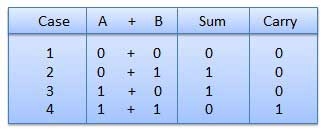
Rules of Binary addition
In fourth step, a sum (1 + 1 = 10) i.e. 0 is written in the given column and a carry of 1 over to the next column is done.
For Example −

Binary addition
Binary Subtraction
Subtraction and Borrow, these are the two words that will be used very frequently for binary subtraction. There rules of binary subtraction are:
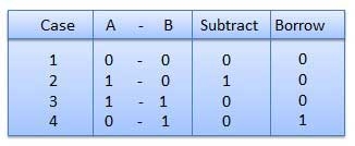
Rules of Binary Subtraction
For Example

Fig.4 Binary subtraction
Binary Multiplication
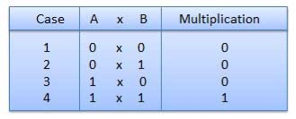
Rules of Binary Multiplication
For Example
Fig.6 Binary Multiplication
Binary Division
For Example
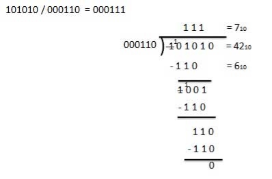
Binary Division
S.N. | Complement | Description |
1 | Radix Complement | It is referred to as the r's complement. |
2 | Diminished Radix Complement | It is referred to as the (r-1)'s complement. |
1's complement
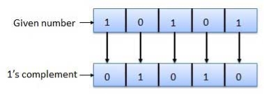
1's complement
2's complement
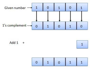
2's complement
Advantages of Binary Code
Classification of binary codes
The codes are broadly classified as:
Weighted Codes
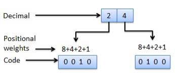
Fig.15: Weighted codes (Ref. 1)
Non-Weighted Codes
1.Excess-3 code

Example
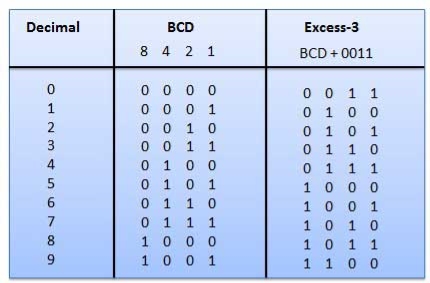
Fig.16: BCD to XS 3 conversion (Ref. 1)
2.Gray Code
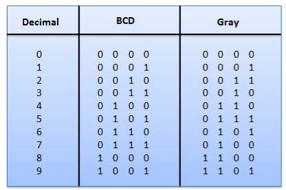
Fig.17: Gray codes (Ref. 1)
Application of Gray code
3. Binary Coded Decimal (BCD) code
But in BCD code only first ten of these numbers are used (0000 to 1001) and rest are invalid. 
Fig.18: BCD codes (Ref. 1)
Advantages of BCD Codes
Disadvantages of BCD Codes
4. Alphanumeric codes
5. Error Codes
Error Code | Description |
Error detection and correction code techniques |
Codes Conversion
Various conversion techniques are:
Binary to BCD Conversion
For Example –
convert (11101)2 to BCD.
Step 1 − Convert to Decimal
Binary Number − 111012
Its Decimal Equivalent −
Step | Binary Number | Decimal Number |
Step 1 | 111002 | ((1 × 24) + (1 × 23) + (1 × 22) + (0 × 21) + (0 × 20))10 |
Step 2 | 111002 | (16 + 8 + 4 + 0 + 0)10 |
Step 3 | 111002 | 2810 |
Binary Number − 111002 = Decimal Number − 2810
Step 2 -- Convert to BCD
Decimal Number − 2810
Its BCD Equivalent:
Step | Decimal Number | Conversion |
Step 1 | 2810 | 00102 10002 |
Step 2 | 2810 | 00101000BCD |
Result
(11100)2 = (00101000)BCD
BCD to Binary Conversion
For Example –
convert (00101001)BCD to Binary.
Step 1 - Converting to BCD
BCD Number − (00101001)BCD
Its Decimal Equivalent.
Step | BCD Number | Conversion |
Step 1 | (00101001)BCD | 00102 10012 |
Step 2 | (00101001)BCD | 210 910 |
Step 3 | (00101001)BCD | 2910 |
Step 2 - BCD Number − (00101001)BCD = Decimal Number − 2910
Converting to Binary by Using long division method.
Decimal Number − 2910
Calculating Binary Equivalent −
Step | Operation | Result | Remainder |
Step 1 | 29 / 2 | 14 | 1 |
Step 2 | 14 / 2 | 7 | 0 |
Step 3 | 7 / 2 | 3 | 1 |
Step 4 | 3 / 2 | 1 | 1 |
Step 5 | 1 / 2 | 0 | 1 |
So, Decimal Number − 2910 = Binary Number − 111012
Result
(00101001)BCD = (11101)2
BCD to Excess-3
For Example –
convert (1000)BCD to Excess-3.
Step 1 − Convert to decimal
(1000)BCD = 810
Step 2 − Add 3 to decimal
(8)10 + (3)10 = (11)10
Step 3 − Convert to Excess-3
(11)10 = (1011)2
Result
(1000)BCD = (1011)XS-3
Excess-3 to BCD Conversion
For Example –
convert (10011000)XS-3 to BCD.
Given XS-3 number = 1 0 0 1 1 0 0 0
Subtract (0011)2 = 0 0 1 1 0 0 1 1
--------------------
BCD = 0 1 1 0 0 1 0 1
Result
(10011000)XS-3 = (01100101)BCD
Errors and Error Correcting Codes
- When bits are being transmitted over the computer network, they get corrupted due to interference and network problems.
- These corrupted bits leads to spurious data that is being received by the receiver and are called errors.
- Hence the Error-correcting codes (ECC) are a sequence of numbers which are generated by specific algorithms for detecting and removing errors in data that can be transmitted over various noisy channels.
- They ascertain the exact number of bits that has been corrupted and the also their location in algorithm.
ECCs are of two types −
- Block codes − The message is divided into fixed-sized blocks of bits which are added for error detection or correction.
- Convolutional codes − The message consists of data streams of arbitrary length and parity symbols are being generated by sliding the application of a Boolean function to the data stream.
Digital logic families
TTL
1) Transistor-transistor logic (TTL) is a class of integrated circuits that maintains logic states and switches with the help of bipolar transistors.
2) It inputs rise to the logic "1" if left unconnected. It is one of the reasons that integrated circuits are widely used, as they are cheap, reliable and faster than RTL and DTL.
3) TTL makes use of transistors with multiple emitters in gates having multiple inputs.
4) The family of TTL is as follows:
It is used for 3.3-volt power supplies and memory interfacing.
It has faster switching than (6ns) but significantly higher power dissipation (22 mW).
It uses Schottky diode clamps at gate inputs to prevent charge storage and improve switching time.
It is used for high resistance values of low-power TTL and the Schottky diodes provide a good combination of speed (9.5ns) and reduce power consumption (2 mW) too.
It is traded switching speed (33ns) for a reduction in power consumption (1 mW).
It speeds up the low-to-high transition of TTL.
Advantages
Disadvantages
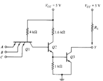
Fig. TTL
CMOS logic
1) The MOSFET (metal-oxide-semiconductor field-effect transistor) are of two types : PMOS (p-type MOS) and NMOS (n-type MOS).
2) A new type of MOSFET logic is made combining both the PMOS and NMOS processes and is called as complementary MOS (CMOS).
3) CMOS stands for “Complementary Metal Oxide Semiconductor”.
4) It is one of the most popular technology in the chip design industry and is used today to form integrated circuits or various applications.
5) Computer memories, CPUs and cell phones make use of this technology due to various advantages. This technology uses both P and N channel semiconductor devices.
Advantages
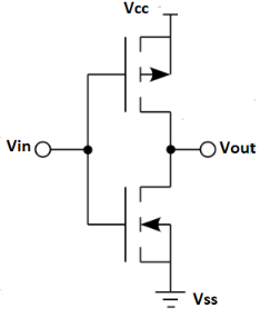
Fig. CMOS
CMOS
1) CMOS stands for “Complementary Metal Oxide Semiconductor”.
2) Computer memories, CPUs and cell phones make use of this technology due to various advantages. This technology uses both P and N channel semiconductor devices.
TTL
1) TTL is a standard method of construction for the processors of mini-computer and mainframe processors.
2) TTL gate works as an analog amplifier.
In digital electronics three-state, tri-state, or 3-state logic allows an output port to assume a high impedance state, effectively removing the output from the circuit, in addition to the 0 and 1 logic levels.
INPUT | OUTPUT |
|
A | B | C |
0 | 0 | Z (high impedance) |
1 | 0 | Z (high impedance) |
0 | 1 | 0 |
1 | 1 | 1 |

Reference
1. R. P. Jain, "Modern Digital Electronics", McGraw Hill Education, 2009.
2. M. M. Mano, "Digital logic and Computer design", Pearson Education India, 2016.
3. A. Kumar, "Fundamentals of Digital Circuits", Prentice Hall India, 2016.