Unit -2
Combinational Digital Circuits
Boolean Postulates
x + 0 = x
x + 1 = 1
x + x = x
x + x’ = 1
x.1 = x
x.0 = 0
x.x = x
x.x’ = 0
Key Takeaways:
simplifying K-maps:
The process of simplifying the algebraic expression of a boolean function is called minimization. Minimization is important since it reduces the cost and complexity of the associated circuit.
For example, the function can be minimized. The circuits associated with above expressions is –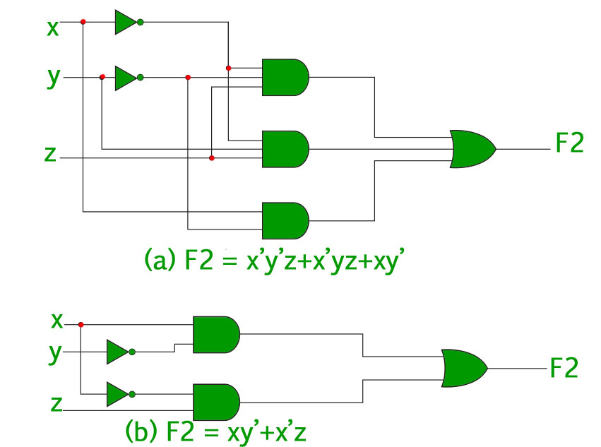
It is clear from the above image that the minimized version of the expression takes a less number of logic gates and also reduces the complexity of the circuit substantially.
Minimization is hence important to find the most economic equivalent representation of a Boolean function.
Minimization can be done using Algebraic Manipulation or K-Map method. Each method has it’s own merits and demerits.
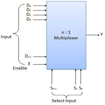
Block diagram of multiplexer
Multiplexers come in multiple variations
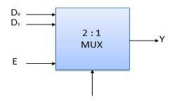
Block Diagram of 2:1 MUX
Truth Table of 2:1 MUX
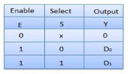
Where x is don’t care.
Key Takeaways
DE- MULTIPLEXER
Various Demultiplexers are used as:
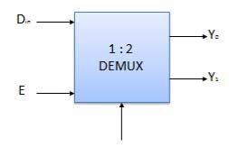
Block diagram
Truth Table
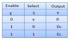
Where x is don’t care.
Key Takeaways:
Block diagram
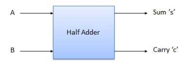
Half adder
Truth Table
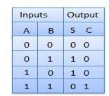
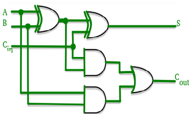
Circuit Diagram
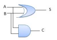
Half adder
Full Adder
Block diagram
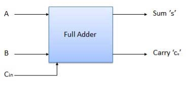
Full adder
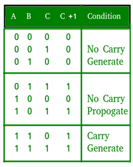
Truth Table
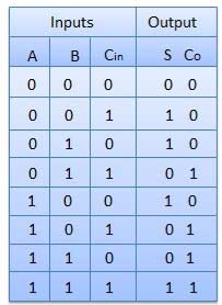
Circuit Diagram
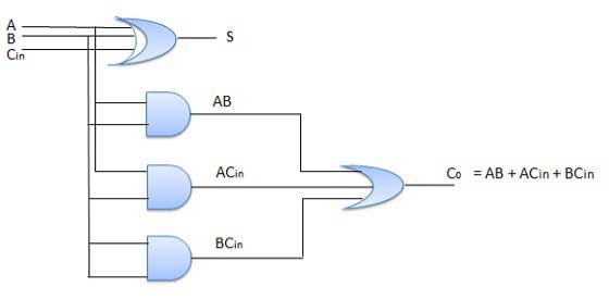
Full adder
Key Takeaways:
Subtractor
Truth Table
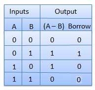
Circuit Diagram
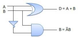
Half subtractor
B. Full Subtractors
Truth Table
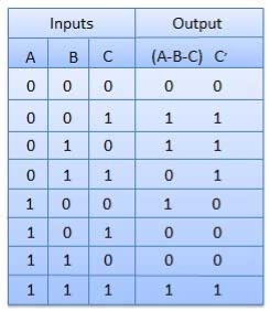
Circuit Diagram
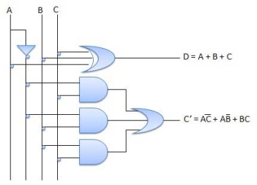
Full subtractor
Key Takeaways:
A decimal number contains 10 digits (0-9). Now the equivalent binary numbers can be found out of these 10 decimal numbers. In case of BCD the binary number formed by four binary digits, will be the equivalent code for the given decimal digits. In BCD we can use the binary number from 0000-1001 only, which are the decimal equivalent from 0-9 respectively.
Let, (12)10 be the decimal number whose equivalent Binary coded decimal will be 00010010. Four bits from L.S.B is binary equivalent of 2 and next four is the binary equivalent of 1.
BCD Addition
Example 1
Let, 0101 is added with 0110.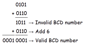
Check your self.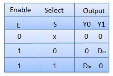
Example 2
Let 0001 0011 is added to 0010 0110.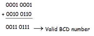

So no need to add 6 as because both  are less than (9)10.
This is the process of BCD Addition.
BCD Subtraction
Example: – 1
Let 0010 0001 0110 is subtracted from 0101 0100 0001.
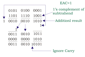
Therefore, 
Check.
We know that 541 − 216 = 325, Thus we can say that our result of BCD Subtraction is correct.

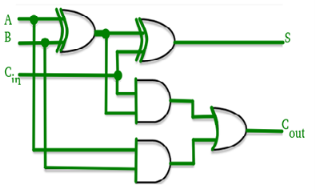
Look ahead Carry adder
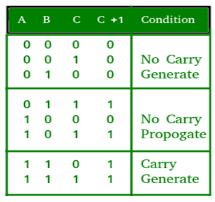
Advantages and Disadvantages of Carry Look-Ahead Adder :
Advantages –
Disadvantages –
Key Takeaways:
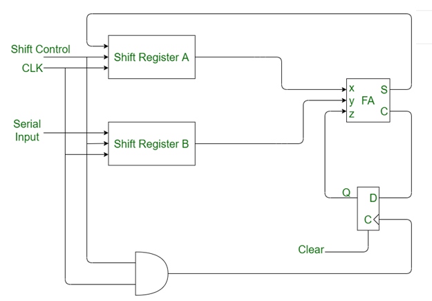
Serial binary adder is a combinational logic circuit that performs the addition of two binary numbers in serial form. Serial binary adder performs bit by bit addition. Two shift registers are used to store the binary numbers that are to be added.
A single full adder is used to add one pair of bits at a time along with the carry. The carry output from the full adder is applied to a D flip-flop. After that output is used as carry for next significant bits. The sum bit from the output of the full adder can be transferred into a third shift register.
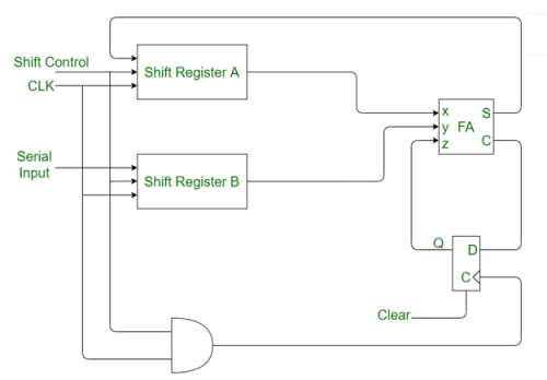
Fig: Block diagram of Serial Binary Adder
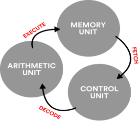
An illustration of the fetch-decode-execute cycle
MSI chips have less than 500 components or have more than 10 but less than 100 gates.
Although medium-scale integration has been replaced by other methods for the regular creation of microchips, recent news shows that engineers have been using carbon nanotube methods to develop new kinds of microchips on a medium-scale integration level.
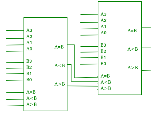
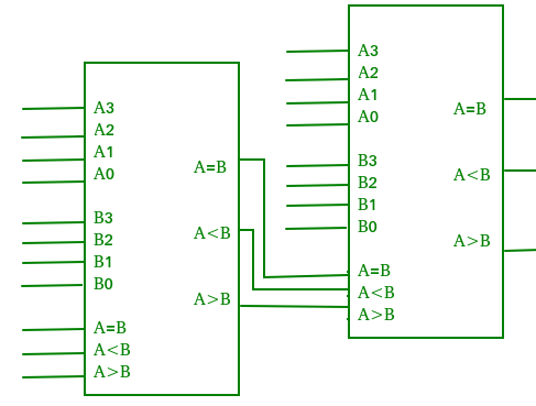
Digital comparator
Applications of Comparators –
Even Parity Generator
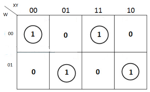
A 3-bit message is transmitted with an even parity bit. Hence assuming, the three inputs W,X and Y that are applied to the circuits and output bit is the parity bit P. The total number of 1s must be even, to generate the even parity bit P.
3- bit message | Even Parity | ||
W | X | Y | P |
0 | 0 | 0 | 0 |
0 | 0 | 1 | 1 |
0 | 1 | 0 | 1 |
0 | 1 | 1 | 0 |
1 | 0 | 0 | 1 |
1 | 0 | 1 | 0 |
1 | 1 | 0 | 0 |
1 | 1 | 1 | 1 |
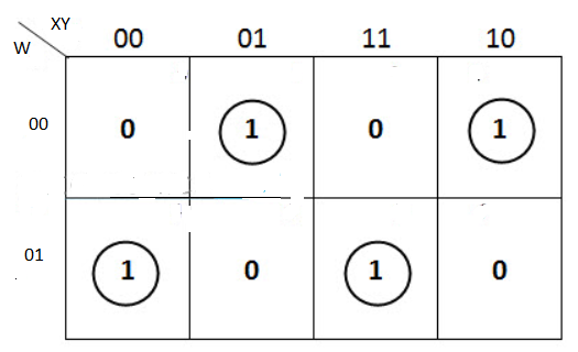
The K-map simplification for 3-bit message even parity generator is
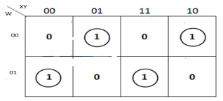
From the above K-Map, the expression is:
P=W′X′Y+W′XY′+WX′Y′+WXY
P=W′(X′Y+XY′)+W(X′Y′+XY)
P=W′(X⊕Y)+W(X⊕Y)′=W⊕X⊕Y

Odd Parity Generator
Considering that the 3-bit data is transmitted with an odd parity bit. The three inputs are W, X and Y and P is the output parity bit. The total number of bits must be odd in order to generate the odd parity bit.
3- bit message | Odd Parity | ||
W | X | Y | P |
0 | 0 | 0 | 1 |
0 | 0 | 1 | 0 |
0 | 1 | 0 | 0 |
0 | 1 | 1 | 1 |
1 | 0 | 0 | 0 |
1 | 0 | 1 | 1 |
1 | 1 | 0 | 1 |
1 | 1 | 1 | 0 |
The K-map simplification for 3-bit message even parity generator is
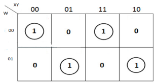

Parity Checker
Even parity checker
Assume a 3-bit binary input, W, X and Y is transmitted along with an even parity bit, P. So, the resultant data contains 4 bits, that is received as the input of even parity checker.
It generates an even parity bit, E. This bit is zero, if the received data contains an even number of ones, which indicates that there is no error in the received data and vice versa.
The Truth table of an even parity checker is:
4-bit Received Data WXYP | Even Parity Check bit E |
0000 | 0 |
0001 | 1 |
0010 | 1 |
0011 | 0 |
0100 | 1 |
0101 | 0 |
0110 | 0 |
0111 | 1 |
1000 | 1 |
1001 | 0 |
1010 | 0 |
1011 | 1 |
1100 | 0 |
1101 | 1 |
1110 | 1 |
1111 | 0 |
The Boolean function of even parity check bit as
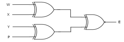
E = W xor X xor Y xor P
The following figure shows the circuit diagram of even parity checker.
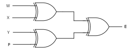
Odd Parity Checker
Assume a 3-bit binary input, W, X and Y is transmitted along with an odd parity bit, P. So, the resultant data contains 4 bits, that is received as the input of odd parity checker.
It generates an odd parity bit, E. This bit is zero, if the received data contains an odd number of ones, which indicates there is no error in the received data.
Key Takeaways:
. Binary To Gray Code

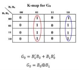
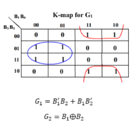
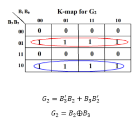
For this circuit, B3 B2 B1 B0 are inputs while G3 G2 G1 G0 are outputs.
K-map for the outputs:
And G3 = B3

2. Gray To Binary Code
Then the K-maps:

And B3 = G3
The realization of Gray-to-Binary converter is
Key Takeaways:
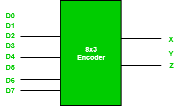
8X3 Encoder
Truth Table –
D7 | D6 | D5 | D4 | D3 | D2 | D1 | D0 | X | Y | Z |
0 | 0 | 0 | 0 | 0 | 0 | 0 | 1 | 0 | 0 | 0 |
0 | 0 | 0 | 0 | 0 | 0 | 1 | 0 | 0 | 0 | 1 |
0 | 0 | 0 | 0 | 0 | 1 | 0 | 0 | 0 | 1 | 0 |
0 | 0 | 0 | 0 | 1 | 0 | 0 | 0 | 0 | 1 | 1 |
0 | 0 | 0 | 1 | 0 | 0 | 0 | 0 | 1 | 0 | 0 |
0 | 0 | 1 | 0 | 0 | 0 | 0 | 0 | 1 | 0 | 1 |
0 | 1 | 0 | 0 | 0 | 0 | 0 | 0 | 1 | 1 | 0 |
1 | 0 | 0 | 0 | 0 | 0 | 0 | 0 | 1 | 1 | 1 |
Implementation –
X = D4 + D5 + D6 + D7
Y = D2 +D3 + D6 + D7
Z = D1 + D3 + D5 + D7
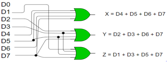
Fig: 12 8:3 encoder (ref.2)
Key Takeaways:
Truth Table –
X | Y | Z | D0 | D1 | D2 | D3 | D4 | D5 | D6 | D7 |
0 | 0 | 0 | 1 | 0 | 0 | 0 | 0 | 0 | 0 | 0 |
0 | 0 | 1 | 0 | 1 | 0 | 0 | 0 | 0 | 0 | 0 |
0 | 1 | 0 | 0 | 0 | 1 | 0 | 0 | 0 | 0 | 0 |
0 | 1 | 1 | 0 | 0 | 0 | 1 | 0 | 0 | 0 | 0 |
1 | 0 | 0 | 0 | 0 | 0 | 0 | 1 | 0 | 0 | 0 |
1 | 0 | 1 | 0 | 0 | 0 | 0 | 0 | 1 | 0 | 0 |
1 | 1 | 0 | 0 | 0 | 0 | 0 | 0 | 0 | 1 | 0 |
1 | 1 | 1 | 0 | 0 | 0 | 0 | 0 | 0 | 0 | 1 |
Implementation
D0 is high when X = 0, Y = 0 and Z = 0. Hence,
D0 = X’ Y’ Z’
Similarly,
D1 = X’ Y’ Z
D2 = X’ Y Z’
D3 = X’ Y Z
D4 = X Y’ Z’
D5 = X Y’ Z
D6 = X Y Z’
D7 = X Y Z
Hence,
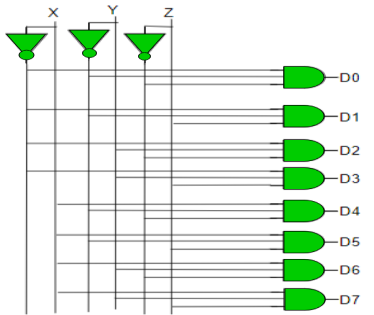
Decoder
Key Takeaways:
xy + xy’ = x(y + y’) = x.1 = x
Procedure of Quine-McCluskey Tabular Method
Steps for simplifying Boolean functions using Quine-McCluskey method:
Example
Simplify, f(W,X,Y,Z)=∑m(2,6,8,9,10,11,14,15) and f(W,X,Y,Z)=∑m(2,6,8,9,10,11,14,15)
using Quine-McClukey tabular method.
Solution:
Group Name | Min terms | W | X | Y | Z |
GA1 | 2 | 0 | 0 | 1 | 0 |
8 | 1 | 0 | 0 | 0 | |
GA2 | 6 | 0 | 1 | 1 | 0 |
9 | 1 | 0 | 0 | 1 | |
10 | 1 | 0 | 1 | 0 | |
GA3 | 11 | 1 | 0 | 1 | 1 |
14 | 1 | 1 | 1 | 0 | |
GA4 | 15 | 1 | 1 | 1 | 1 |
Group Name | Min terms | W | X | Y | Z |
GB1 | 2,6 | 0 | - | 1 | 0 |
2,10 | - | 0 | 1 | 0 | |
8,9 | 1 | 0 | 0 | - | |
8,10 | 1 | 0 | - | 0 | |
GB2 | 6,14 | - | 1 | 1 | 0 |
9,11 | 1 | 0 | - | 1 | |
10,11 | 1 | 0 | 1 | - | |
10,14 | 1 | - | 1 | 0 | |
GB3 | 11,15 | 1 | - | 1 | 1 |
14,15 | 1 | 1 | 1 | - | |
|
|
|
|
|
|
Group Name | Min terms | W | X | Y | Z |
GB1 | 2,6,10,14 | - | - | 1 | 0 |
2,10,6,14 | - | - | 1 | 0 | |
8,9,10,11 | 1 | 0 | - | - | |
8,10,9,11 | 1 | 0 | - | - | |
GB2 | 10,11,14,15 | 1 | - | 1 | - |
10,14,11,15 | 1 | - | 1 | - | |
|
|
|
|
|
|
Group Name | Min terms | W | X | Y | Z |
GC1 | 2,6,10,14 | - | - | 1 | 0 |
| 8,9,10,11 | 1 | 0 | - | - |
GC2 | 10,11,14,15 | 1 | - | 1 | - |
Therefore, the prime implicants are YZ’, WX’ & WY.
The prime implicant table is shown below.
Min terms / Prime Implicants | 2 | 6 | 8 | 9 | 10 | 11 | 14 | 15 |
YZ’ | 1 | 1 |
|
| 1 |
| 1 |
|
WX’ |
|
| 1 | 1 | 1 | 1 |
|
|
WY |
|
|
|
| 1 | 1 | 1 | 1 |
The reduced prime implicant table is shown below.
Min terms / Prime Implicants | 8 | 9 | 11 | 15 |
WX’ | 1 | 1 | 1 |
|
WY |
|
| 1 | 1 |
Min terms / Prime Implicants | 15 |
WY | 1 |
Hence, f(W,X,Y,Z) = YZ’ + WX’ + WY.
Simplify
Y(A,B,C,D) =∑ m(0,1,3,7,8,9,11,15)
Groups are made with respect to the no. of one’s present.
Now, comparing with the above table wherever we have a different bit present we put a ’-‘ there.

The same thing is done by comparing from the above table.
The table for prime implicants is:

Rounding the min terms which has X in column and hence the final answer is B’C’ + CD.
Reference
1. R. P. Jain, "Modern Digital Electronics", McGraw Hill Education, 2009.
2. M. M. Mano, "Digital logic and Computer design", Pearson Education India, 2016.
3. A. Kumar, "Fundamentals of Digital Circuits", Prentice Hall India, 2016.