Unit -3
Sequential circuits and systems
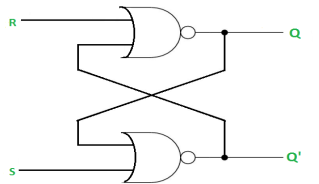
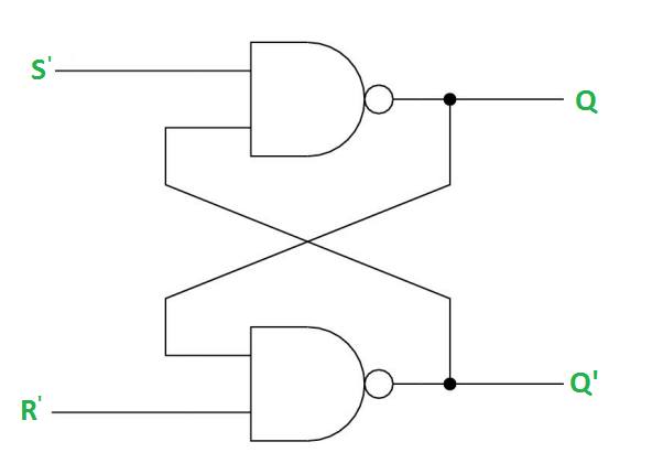
A latch is a simple digital circuit where the output can be set to either logic 1 or logic 0 by an input signal. The circuit then remains in this state even after the input is removed. This is a memory circuit that can “remember” a single binary digit (bit).
SR Latch is a circuit which has:
(i) 2 cross-coupled NOR gate or NAND gate.
(ii) 2 input S for SET and R for RESET.
(iii) 2 output Q and Q’.
Q | Q’ | STATE |
1 | 0 | Set |
0 | 1 | Reset |
Under normal conditions, both the input remains 0.
RS Latch with NAND gates:
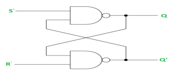
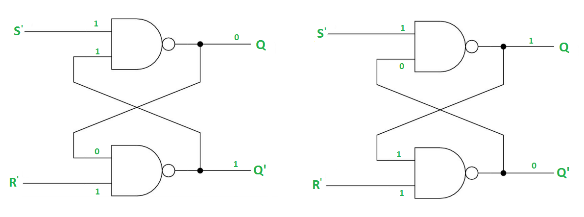
Case-1: When S’=R’=1 or S=R=0 then
If Q = 1, Q = R’ = 1.
If Q = 0, Q = 0 and R’ = 1 respectively.
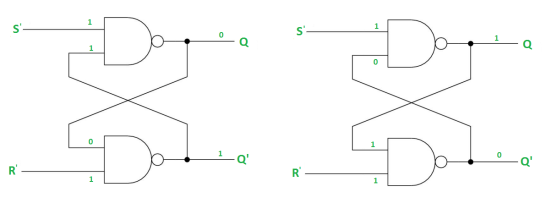
Case-2: S’=0, R’=1 (S=1, R=0)
As S’=0, Q = 1(SET state).
In 2nd NAND gate, as Q = R’ = 1, Q’=0.
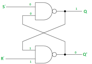
Case-3: S’= 1, R’= 0 (S=0, R=1)
As R’=0, Q’ = 1.
In 1st NAND gate, as Q =S’ = 1, Q=0 (RESET state).
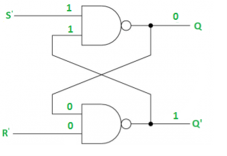
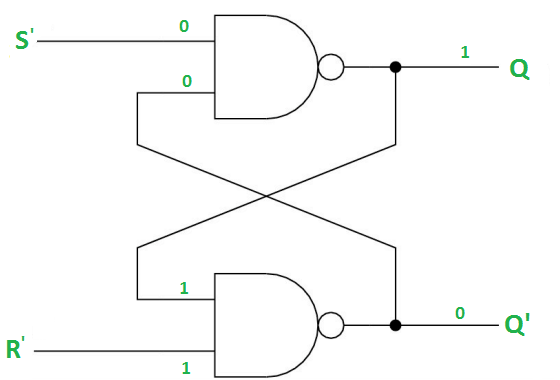
Case-4: S’= R’= 0 (S=R=1)
When S=R=1, both Q = Q’ = 1 which is not allowed.
So, this input condition is prohibited.
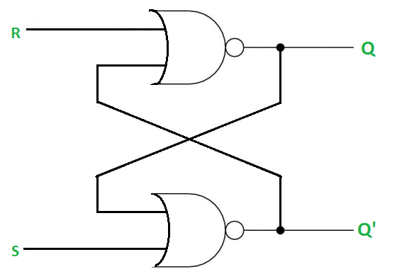
The SR Latch using NOR gate is:
Gated SR Latch –
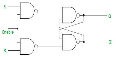
It is a latch which enable input that works when enable = 1 and retain the previous state when enable = 0.
Gated D Latch –
It is similar to SR latch with little modifications. Here, the inputs are complements of one another. The design of D latch with Enable signal is given below:
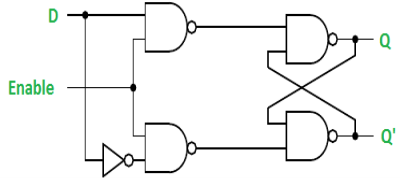
The truth table is shown below:
ENABLE | D | Q(N) | Q(N+1) | STATE |
1 | 0 | x | 0 | RESET |
1 | 1 | x | 1 | SET |
0 | x | x | Q(n) | No Change |
As the output is same as input, it is also known as Transparent Latch.
The characteristic equation for D latch with enable input is given as:
Q(n+1) = EN.D + EN'.Q(n)
J-K Flip Flop:

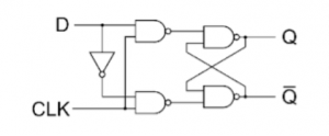
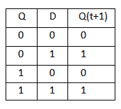
D Flip Flop
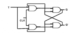
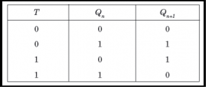
T Flip Flop :
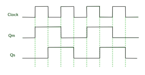
Timing Diagram of a Master flip flop –
Conversion for FlipFlops :-
EXCITATION TABLE:
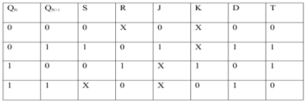
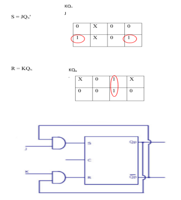
i) SR To JK FlipFlop
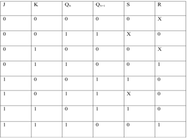
Excitation Functions:
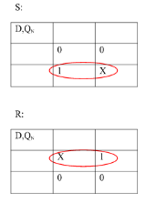
ii) Convert SR To D FlipFlop:
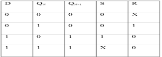
Excitation Functions:
S = D
R = D‘
The registers which shift the bits towards right are called “Shift right registers”.
Shift registers are of 4 types and they are:

Ring counter
For non overlapping case
Input :0110101011001
Output:0000100010000
For overlapping case
Input :0110101011001
Output:0000101010000
The steps to design non-overlapping 101 Mealy sequence detector are:
Step 1: Development of the state diagram –
The state diagram of a Mealy machine for a 101 sequence detector is:
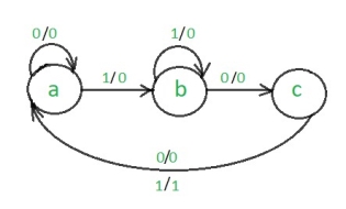
Step 2: Assignment of the code–
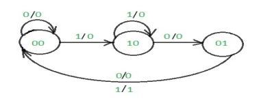
Rule 1 : States having the same next states for a given input condition should have adjacent assignments.
Rule 2:States that are the next states to a single state must be given adjacent assignments.
Rule 1 given preference over Rule 2.

The state diagram after the code assignment is:
Step 3: Making Present State/Next State table –
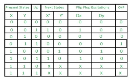
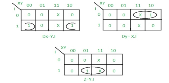
Step 4: Draw K-maps for Dx, Dy and output (Z) –
Step 5: Final implementation of the circuit –
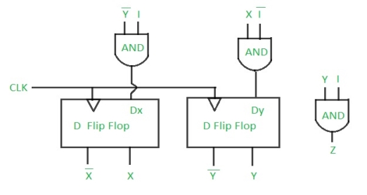
This is the desired circuit for a Mealy 101 non overlapping sequence detector.
In this universal clock is not used and only the first flip flop is driven by main clock and the clock input of rest of the following is driven by output of previous flip flops.

Asynchronous counter

Timing diagram of Asynchronous counter
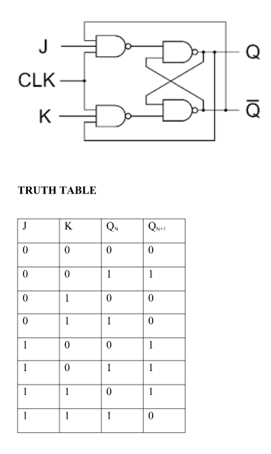
synchronous counter
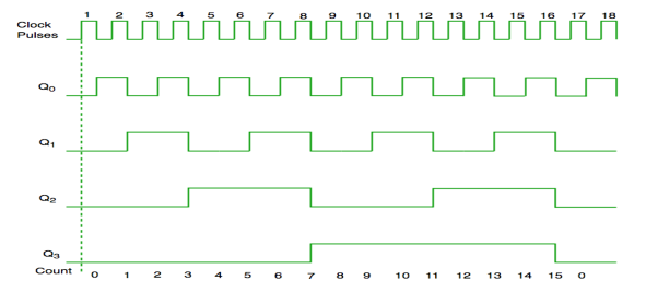
Timing diagram of synchronous counter
Asynchronous (Ripple) Counters:
Synchronous Counters:
In this universal clock is not used and only the first flip flop is driven by main clock and the clock input of rest of the following is driven by output of previous flip flops. 
Asynchronous counter

Timing diagram of Asynchronous counter
In this way ripples are generated through Q0,Q1,Q2,Q3 and therefore it is also called as a RIPPLE counter.
Reference
1. R. P. Jain, "Modern Digital Electronics", McGraw Hill Education, 2009.
2. M. M. Mano, "Digital logic and Computer design", Pearson Education India, 2016.
3. A. Kumar, "Fundamentals of Digital Circuits", Prentice Hall India, 2016.