Unit - 1
Power Switching Devices
A power diode is commonly used in power electronics circuits just like a regular diode. A power diode has two-terminals and conducts current in one direction. A power diode varies in construction from a standard diode to enable this higher current rating.
In regular diodes (also known as “signal diode”), the doping level of both P and N sides is the same and hence we get a PN junction but in power diodes, we have a junction formed between a heavily doped P+ and a lightly doped N– the layer which is epitaxially grown on a heavily doped N+ layer. Hence the structure looks as shown in the figure below.
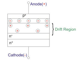
Figure 1. Power Switching Devices
The N– layer is the key feature of the power diode which makes it suitable for high power applications. This layer is very lightly doped, almost intrinsic and hence the device is also known as PIN diode where i stands for intrinsic.
As we can see in the figure above that the net charge neutrality of the space charge region is still maintained as was the case in the signal diode but the thickness of the space charge region is quite high and deeply penetrated into the N region.
This is due to its light doping concentration, as we know that the thickness of the space charge region increases with a decrease in doping concentration.
In order to trigger the switching current is removed hence we need another device because here the transistor fails. Thyristor solves this issue also besides handling current it can run continuously even if switching current is removed.
In a thyristor, the silicon wafer is doped with four alternate P and N types, which looks like two transistors connected back-to-back as shown in figure below.
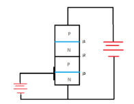

Figure 2. Thyristor
Here, the P (cathode) and the N (anode) are joined in series, thus we get three terminal pins: anode, gate and cathode.
When we forward bias the anode and cathode i.e., anode and cathode connected to the positive and negative terminals of a battery, the first PN junction and last PN junction (j1 and j3) become forward biased due to break of the depletion layer. The junction j2 remains as reversed biased as no current is provided to the gate.
When we supply current to the gate, then the j2 junction layer starts breaking and the current starts flowing in the circuit. When a sufficient positive signal current or pulse is applied to the gate terminal, it triggers the thyristor into a conducting state.
A thyristor can only be fully on or off, means it cannot lie in between On and Off states similar to transistors. This makes a thyristor unsuitable as an analog amplifier, but useful as a switching device.
Its three working modes:
Forward blocking mode
Junctions j1 and j3 are in forward working state while j2 is in reverse biased state and does not allow the current to flow.
Forward conduction mode
Here a positive voltage is applied to the gate terminal, causing the j2 depletion region to break down. Due to this, current starts flowing in the circuit and results in switch ON mode.
Reverse blocking mode
Here we give negative voltage to anode and positive voltage to cathode while the gate is kept in an open circuit, causing j1 and j3 to be in reverse bias and j2 in forward bias. As j1 and j2 are reverse biased, the flow of current is not possible.
The MOSFET is a four-terminal device with source(S), gate (G), drain (D) and body (B) terminals. The body of the MOSFET is frequently connected to the source terminal making it a three- terminal device like field effect transistor.
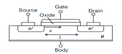
Figure 3. MOSFET
The MOSFET works by varying the width of a channel along which charge carriers flow (electrons or holes). The charge carriers enter the channel at source and exit via the drain.
The width of the channel is controlled by the voltage on an electrode is called gate which is located between source and drain. It is insulated from the channel near an extremely thin layer of metal oxide.
The MOS capacity present in the device is primary.
The MOSFET can function in two ways
Depletion Mode:
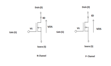
Figure 4. Depletion mode
When there is no voltage on the gate, the channel displays maximum conductance. As the voltage on the gate is either positive or negative, the channel conductivity decreases.
Enhancement Mode
When there is no voltage on the gate the device does not conduct. More is the voltage on the gate, the better the device can conduct.
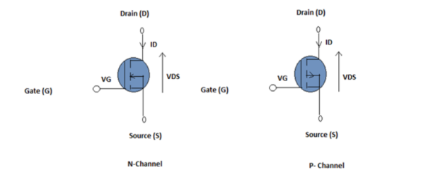
Figure 5. Enhancement mode
Working:
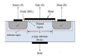
Figure 6. MOSFET construction
P-channel MOSFET
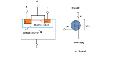
Enhanced mode
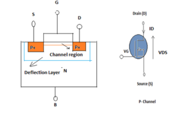
Depletion mode
Figure 7. P channel MOSFET
N- Channel MOSFET:
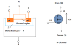
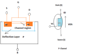
Figure 8. Depletion mode
A typical switching circuit of IGBT is shown below, the gate volt VG is applied to the gate pin to switch a motor (M) from a supply voltage V+. The resistor Rs is roughly used to limit the current through the motor.
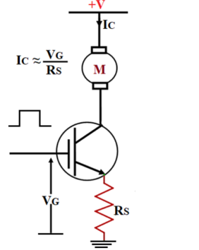
Figure 9. Switching characteristics
The input characteristics of IGBT can be understood from the graph below.
Initially, when no voltage is applied to the gate pin the IGBT is in turn off condition and no current flows through the collector pin. When the voltage applied to the gate pin exceeds the threshold voltage, the IGBT starts conducting and the collector current IG starts to flow between the collector and emitter terminals. The collector current increases with respect to the gate voltage as shown in the graph below.
I-V characteristics:
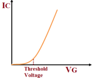
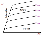
Figure 10. I-V characteristics
Applications of IGBT
The resistor RE is chosen so that the load line determined by RE passes through the device characteristic in the negative resistance region to the right of the peak point but to the left of the valley point as shown in figure.
If the load line does not pass to the right of the peak point P, the device cannot turn on.
For ensuring turn-on of UJT RE < VBB – Vp / IP This can be established as below Consider the peak point at which IRE = Ip and VE = VP.
Then VE = VBB – IRE RE. So, RE(MAX)= VBB – VE / IRE = VBB – Vp / IP at the peak point.
At the valley point, V IE = IV and VE = VV so that VE = VBB – IRE RE
So, RE(MIN) = VBB – VE / IRE = VBB – VV / IV or for ensuring turn-off.
RE > = VBB – VV / IV.
So, the range of resistor RE is given as VBB – VP / IP >RE > VBB – VV / IV.
The resistor R is chosen small enough so as to ensure that SCR is not turned on by voltage VR when emitter terminal E is open or IE = 0.
The voltage VR = RVBB/R + RBB for open-emitter terminal. The capacitor C determines the time interval between triggering pulses and the time duration of each pulse.
By varying RE, we can change the time constant RE C and alter the point at which the UJT fires. This allows us to control the conduction angle of the SCR, which means the control of load current.
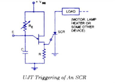
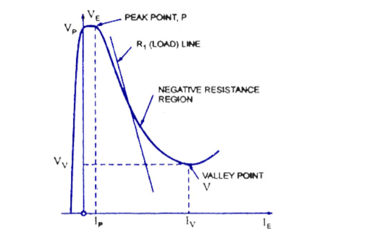
Figure 11. Firing circuit of Thyristor
1.6.1 Voltage commutation
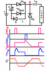
Figure 12. A voltage commutated DC-DC Chopper and most significant waveforms.
ThM is the main SCR and ThAux is the Auxiliary. As a consequence of the previous cycle, Capacitor C is charged with the dot as positive. When the Main SCR is triggered, it carries the load current, which is held practically level by the large filter inductance, LF and the Free-wheeling diode. Additionally, the charged Capacitor swings half a cycle through ThM, L and D ending with a negative at the dot.
The reverse voltage may be less than its positive value as some energy is lost in the various components in the path. The half cycle capacitor current adds to the load current and is taken by the Main SCR.
With the negative at the dot C-ThAux is enabled to commutate ThM. When ThAux is triggered the negative charge of the capacitor is impressed onto ThM and it immediately turns off. The SCR does take the reverse recovery current in the process. Thereafter, the level load current charges the capacitor linearly to the supply voltage with the dot again as positive.
The Load voltage peaks by the addition of the capacitor voltage to the supply when ThAux is triggered. The voltage falls as the capacitor discharges both changes being linear because of the level load current. When the Capacitor voltage returns to zero, the load voltage equals supply voltage. The turn-off time offered by the commutation circuit to the SCR lasts till this stage starting from the triggering of ThAux.
Now the capacitor is progressively positively charged and the load voltage is equally diminished from the supply voltage. ThAux is naturally commutated when the capacitor is fully charged and a small excess voltage switches on the freewheeling diode.
With the positive at the dot the capacitor is again ready for the next cycle. Here ThAux must be switched before ThM to charge C to desired polarity.
1.6.2 Current Commutation
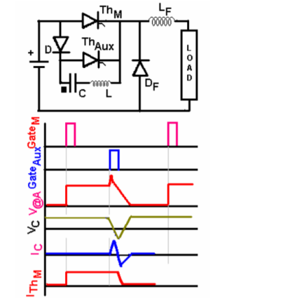
Figure 13. Current Commutation
Turn-off process is consequently accompanied by an overlap between ThM and the diode D in the D-C-L path. Once the main SCR is turned off, the capacitor current becomes level and the voltage decreases linearly. A voltage spike appears across the load when the voltage across the commutating inductance collapses and the capacitance voltage adds to the supply voltage. The Fig. shows current commutated DC-DC Chopper and most significant waveforms The free-wheeling diode also turns on through overlap with D when the capacitor voltage just exceeds the supply voltage and this extra voltage drives the commutating current through the path D-Supply-DF-L. Thus, there is soft switching of all devices during this period.
Figure. shows a basic MOSFET drive circuit. In practice, the capacitance of a MOSFET to be driven and its usage conditions must be considered in designing a drive circuit.
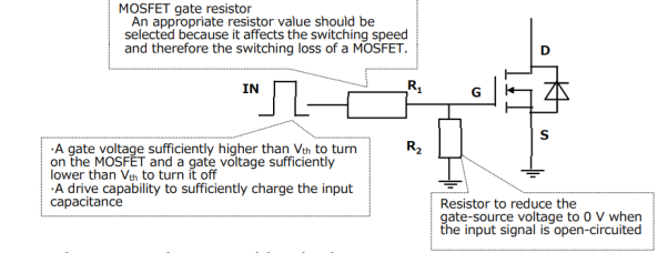
Figure 14. MOSFET drive
There is a growing need for MOSFETs for switching applications (load switches) to provide a conducting path in a circuit only when it is operated, and thereby reduce the power consumption of electronic devices. At present, MOSFETs are directly driven by a logic circuit or a microcontroller in many applications. Figure shows an example of a circuit for turning on and off a power relay. Since turn-on and turn-off times may be as slow as a few seconds for load switches, the MOSFET gate can be driven with a small current.
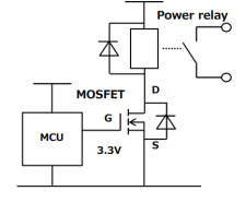
Figure 15. Mosfet Gate drive circuit.
IGBT gate drive
An IGBT driver turns on and off the IGBT very quickly by charging and discharging the small capacitance between the gate and source. It is mostly used when an IGBT is run at rated high frequencies like in switch mode power supply (SMPS).
The IGBT has 3 terminals: - gate, drain and source. The gate controls the flow of current from drain to source.
When the IGBT is manufactured a small capacitor forms between the gate and source terminals. When the signal is given to gate terminal the capacitor charges and allows flow of current from drain to source but if the signal is removed the capacitor between the gate and source stays charged so the gate still allows current to flow from drain to source.
Now the job of the IGBT DRIVER is to discharge this capacitor quickly so that it can turn on again quickly.
If it is not used, then IGBT will not be able to run at high rated frequencies.
References: