Unit - 4
DC-DC boost circuit
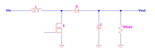
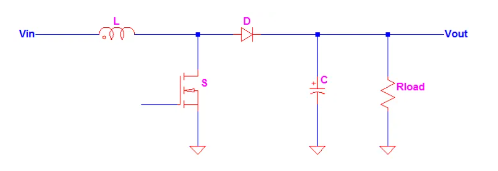
A typical Boost converter is shown below.
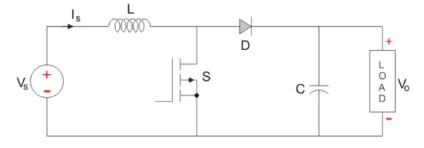
The input voltage source is connected to an inductor. The solid-state device which operates as a switch is connected across the source. The second switch used is a diode. The diode is connected to a capacitor, and the load and the two are connected in parallel as shown in the figure above.
The inductor connected to input source leads to a constant input current, and thus the Boost converter is seen as the constant current input source. And the load can be seen as a constant voltage source.
The controlled switch is turned on and off by using Pulse Width Modulation (PWM). The Boost converter has two modes of operation. The first mode is when the switch is on and conducting.
Mode I: Switch is ON, Diode is OFF
The switch is ON and therefore represents a short circuit ideally offering zero resistance to the flow of current so when the switch is ON all the current will flow through the switch and back to the DC input source. Let us say the switch is on for a time TON and is off for a time TOFF. We define the time period, T, as
T = TON + T OFF
and the switching frequency
f switching = 1/T.
Let us now define another term, the duty cycle,
D = TON/T
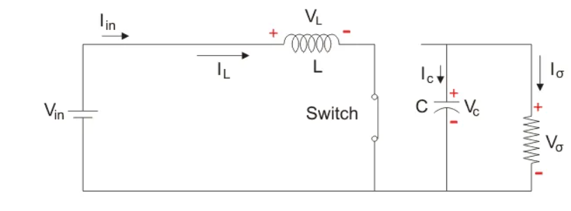
Let us analyze the Boost converter in steady state operation for this mode using KVL.
Vin = VL
VL = L diL /dt = Vin
diL/dt = ∆ iL/∆t = ∆iL/DT = Vin/L
Since the switch is closed for a time Ton = DT we can say that ∆t=DT
(∆ iL) closed= (Vin/L) DT
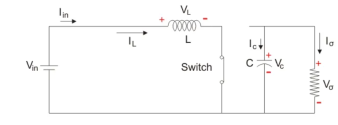
Let us analyze the Boost converter in steady state operation for this mode using KVL. Since the switch is closed for a time TON = DT we can say that Δt = DT.
While performing the analysis of the Boost converter, we have to keep in mind that
Mode II: Switch is OFF, Diode is ON
In this mode, the polarity of the inductor is reversed. The energy stored in the inductor is released and is ultimately dissipated in the load resistance, and this helps to maintain the flow of current in the same direction through the load and also step-up the output voltage as the inductor is now also acting as a source in conjunction with the input source. But for analysis, we keep the original conventions to analyze the circuit using KVL.
Let us now analyse the Boost converter in steady state operation for Mode II using KVL.
Vin = VL + Vo
VL = L diL/dt = Vin -VO
diL/dt = ∆ iL/∆t = ∆ iL / (1-D) T = Vm-Vo/L
Since the switch is open for a time
TOFF = T – TON = T -DT = (1-D) T
We can say that
∆t = (1-D) T
(∆ iL) open = (Vin -Vo/L) (1-D) T
It is already established that the net change of the inductor current over any one complete cycle is zero
(∆ iL) closed + (∆ iL) open =0
(Vin – Vo) /L (1-D) T + (-Vo/L) DT =0
Vo /Vin = 1/ 1-D
Since the switch is open for a time
TOFF = T – TON = T – DT = (1-D) T
We can say that
∆t = (1-D) T
It is already established that the net change of the inductor current over any one complete cycle is zero.
(∆ iL) closed + (∆ iL) open =0
(Vin – Vo/L) (1-D) T + (-Vo/L) DT =0
Vo /Vin = 1/ 1-D
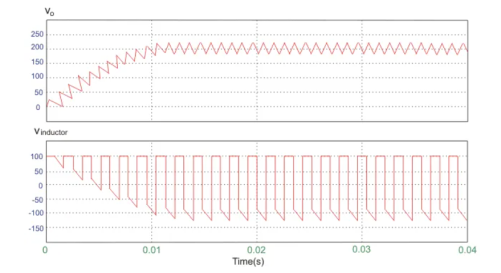
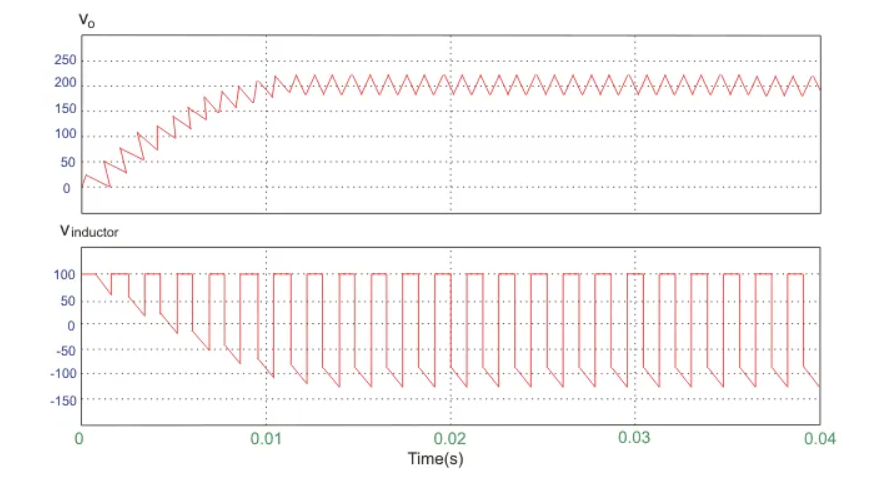
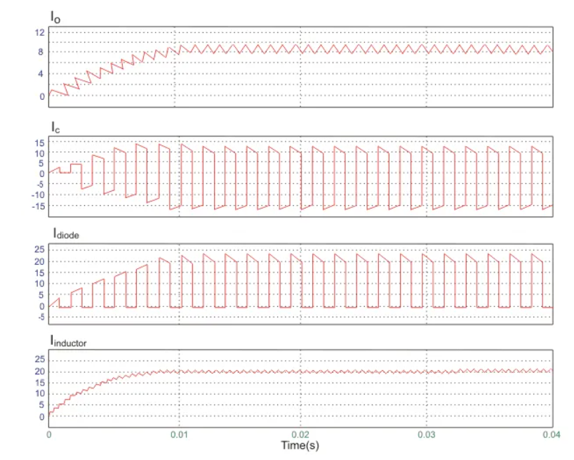
A circuit of a Boost converter and its waveforms are shown below. The inductance, L, is 20mH and the C is 100µF and the resistive load is 20Ω. The switching frequency is 1 kHz. The input voltage is 100V DC and the duty cycle is 0.5.
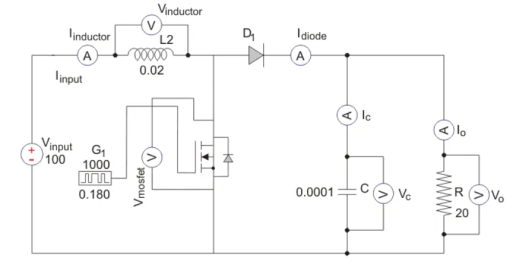

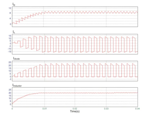
The voltage waveforms are as shown above and the current waveforms are as shown in the figure below.
The voltage waveforms are as shown above and the current waveforms are as shown in the figure below.
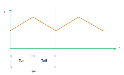
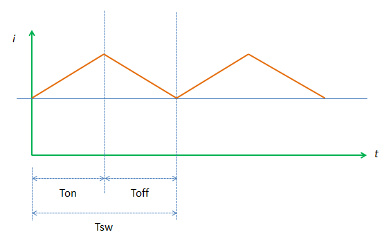
The inductor of the boost converter charges during Ton and discharges during Toff. The inductor current waveform is then resembled like Figure 2 below.
The figure is an inductor waveform of a continuous conduction mode boost converter. A boost converter by the way can operate in three modes; continuous conduction (CCM), discontinuous conduction (DCM) and boundary mode. For CCM the inductor current will not reach zero after every switching cycle. For DCM, the inductor current is reaching zero before the next Ton occur.
How to Calculate the Duty Cycle of Boost Converter – Analysis during Ton
During Ton, the switch S is on. The diode will be reversed biased and this
time the load is being supplied by the energy stored in the capacitor C. The inductor will charge. The flow of the current is from Vin to inductor L then to switch S. By KVL,

Then expressing VL
 -------------------------(1)
The voltage across inductor is also defined by below formula.
 ---------------------------------------(2)
Expressing the change in current di
 ---------------------------------------(3)
Substitute 1 to 3
 ----------------------------------------(4)
Then we will get rid of the variable dt by integrating the equation from 0 to Ton.

 ----------------------------------------------------(5)
How to Calculate the Duty Cycle of Boost Converter – Analysis during Toff
During Toff, the inductor reverses its polarity and the diode at this time will be forward biased and the load will be supplied by the energy in the inductor. The energy on the inductor will start to decay. The flow of current is from Vin to diode D then to the load. Applying KVL,

Expressing VL,
 ------------------------------------------(6)
Substituting [Eq. 6] to [Eq. 3] will result to
 ----------------------------------(7)
Then we will eliminate the variable dt through integration from Ton to T.
 ---------------------------------------(8)

Now go back to Figure 2, the magnitude of the inductor current during Ton and Toff is equal. Therefore, we can equate [Eq. 5] and [Eq. 8].


Then substitute Ton = DT

Then solving for the duty cycle, D
 -----------------------------------------------------(9)
Eq. 9
Assuming ideal values (diode and switch voltage drops are zero)
 ----------------------------------------(10)
Output Voltage:
The relationship of voltage and current for an inductor is:
 , or
, or

For a constant rectangular pulse:
From this we can see that the current is a linear ramp, when the voltage is a constant pulse.
When the transistor switches on the current is:
 , or
, or
and when the transistor switches off the current is:
 , or
, or
 (Equation 1)
Where VD is the voltage drop across the diode, and VTrans is the voltage drop across the transistor. Note that the continuous/discontinuous boundary occurs when io is zero.
By equating through delta i, we can solve for Vout:


We can also solve for the duty cycle as follows,


If we neglect the voltage drops across the transistor and diode then:

So, it is clear that the output voltage is related directly to the duty cycle of the pulses.
References:
