Unit 1
Introdution to 8 bit and 16 bit Microprocessor
A Microprocessor is an important part of a computer architecture without which you will not be able to perform anything on your computer. It is a programmable device that takes in input perform some arithmetic and logical operations over it and produce desired output. In simple words, a Microprocessor is a digital device on a chip which can fetch instruction from memory, decode and execute them and give results.
Microprocessor performs three basic things while executing the instruction:
- It performs some basic operations like addition, subtraction, multiplication, division and some logical operations using its Arithmetic and Logical Unit (ALU). New Microprocessors also perform operations on floating point numbers also.
- Data in Microprocessor can move from one location to another.
- It has a Program Counter (PC) register that stores the address of next instruction based on the value of PC, Microprocessor jumps from one location to another and takes decision.
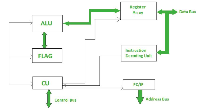
Figure 1. Microprocessor
Computer Architecture refers to those attributes of a system that have a direct impact on the logical execution of a program.
Examples:
o The instruction set of the number of bits used to represent various data types
o I/O mechanisms
o memory addressing techniques
Computer Organization refers to the operational units and their interconnections that realize the architectural specifications.
Examples are things that are transparent to the programmer:
o control signals
o interfaces between computer and peripherals o the memory technology being used
So, for example, the fact that a multiply instruction is available is a computer architecture issue. How that multiply is implemented is a computer organization issue.
Organization is how features are implemented
o Control signals, interfaces, memory technology.
o e.g. Is there a hardware multiply unit or is it done by repeated addition? •
All Intel x86 family share the same basic architecture
• The IBM System/370 family share the same basic architecture
• This gives code compatibility
o At least backwards
• Organization differs between different versions
The assembly level programming 8086 is based on the memory registers. A Register is the main part of the microprocessors and controllers which are located in the memory that provides a faster way of collecting and storing the data. If we want to manipulate data to a processor or controller by performing multiplication, addition, etc., we cannot do that directly in the memory where need registers to process and to store the data. The 8086 microprocessor contains various kinds of registers that can be classified according to their instructions such as general- purpose registers and special purpose registers.
1.3.1 Address bus
The address bus carries address and is one way bus from microprocessor to the memory or other devices. 8085 microprocessors contain 16-bit address bus and are generally identified as A0 - A15. The higher order address lines (A8 – A15) are unidirectional and the lower order lines (A0 – A7) are multiplexed (time-shared) with the eight data bits (D0 – D7) and hence, they are bidirectional.
1.3.2 Data Bus
Data bus carries data in binary form between microprocessor and other external units such as memory. It is used to transmit data that is information, results of arithmetic etc between memory and the microprocessor. Data bus is bidirectional in nature.
1.3.3 Control bus
Control bus are various lines which have specific functions for coordinating and controlling microprocessor operations. The control bus carries control signals partly unidirectional and partly bidirectional.
1.3.4 Tristate bus
Since we can have multiple masters on a bus, we need Tristate logic for attachment to a bus so that each device can choose to drive or not drive the bus depending on whether it is the bus master for a given bus cycle
Tri-state logic prevents a bus conflict where one device is driving a signal to 1 and another device is driving it to 0 at the same time - generates high current through wires.
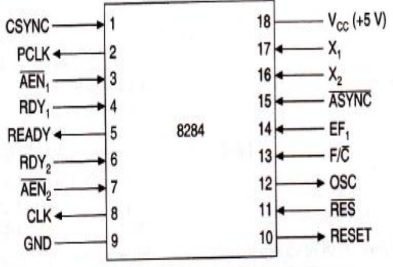
8284 clock generator is an IC developed by Intel to provide clock frequency, ready and reset signal to the 8086/8088 microprocessor. It is an 18 pin chip.8284 produces the clock signal, synchronizes it with the ready and reset signal and provides it to the microprocessor.
Functions of 8284
- It provides a stable clock to the processor.
- In the case of a multiprocessor system, it facilitates synchronization of multiple clock signals.
- Provides resetting to the processor along with the clock signal.
Logic Circuit and Working of 8284 Clock Generator
The figure below shows the block diagram of 8284 Clock Generator:
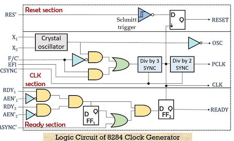
8284 is composed of 3 sections, reset section, clock section and ready section.
OSC, CLOCK and PCLK are the three outputs generated by the clock section. The crystal oscillator present in this section generates a square wave signal as its output when the crystal is attached between its two inputs X1 and X2.
The frequency of the generated square wave signal is equal to the frequency of the crystal.
Further, the square wave signal is fed to AND gate and NOT gate (inverted buffer) simultaneously. This inverted buffer gives the OSC signal.
- F/C’ is frequency/crystal selection pin used to select the input of the oscillator.
When its input is high then the operating frequency is determined by the external frequency input (EFI), while in the other case it is determined by the crystal oscillator.
Through AND gate, the output of the oscillator is fed to the divided by 3 counter when F/C’ is low. While when F/C’ is high, EFI is fed to the counter. Timing signals for ready and reset pins are produced by the counter.
- For the operation with EFI input, synchronization between multiple processor system is necessary, for which CSYNC is used. Whereas when the crystal oscillator decides the operating frequency then, in that case, this signal is subjected to ground.
CSYNC allows synchronization among multiple 8284s. In the case of single 8284, this pin is grounded.
It is to be noted that the generated output clock frequency in both cases will be one-third of the applied input frequency.
The clock signal for peripheral devices is generated by dividing the clock frequency by 2. Basically, the devices like 8254 timers require PCLK as they need lower operating frequency.
The reset section of 8284 is composed of a Schmitt trigger and a D flip-flop. On each negative edge of the clock signal, the circuit applies a reset signal to the processor.
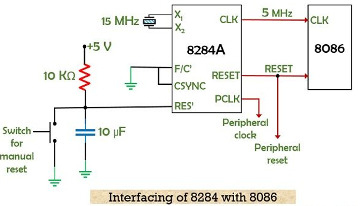
Initially when the power is first applied then the RC circuit gives logic 0 as input to the RES pin as shown in the figure below. But soon the capacitor gets charged to +5 V through th
e resistor.
Also, the operator can anytime reset the processor by making use of the push button.
The ready signals for the processor is produced by the ready section. This gives information regarding whether the processor is ready for operation or not. If the ready signal is low, then this shows the wait state of the processor.
The figure below represents the interfacing of 8284 clock generator with 8086 microprocessor:
Pin Description of 8284
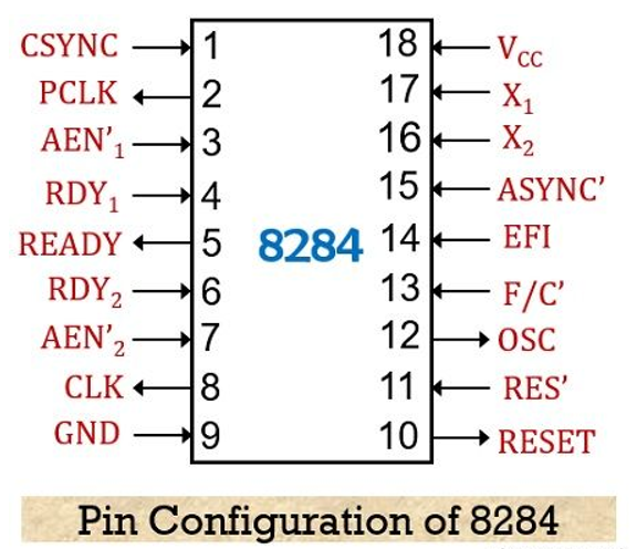
- CSYNC – pin number 1 – Stands for clock synchronization. It is an active high signal that synchronizes the clock signal of various 8284 chips present in a single system. As this pin shows the significance of EFI based operation, thus it is grounded when the crystal is present between the inputs X1 and X2.
- PCLK– pin number 2 – Stands for peripheral clock. An active high signal at this pin provides clock signal of one-sixth frequency of the EFI or crystal frequency to the peripheral devices like 8254.
- AEN1’ and AEN2’ – pin number 3 and 7 – Stands for address enable and are active low pins. It qualifies the bus ready signals i.e., RDY1 and RDY 2.
- RDY1 and RDY 2 – pin number 4 and 6 – These are active high pins and these signals are provided by devices present on the data bus showing the availability or reception of the data.
- READY – pin number 5 – This pin holds the READY signal of 8086 microprocessor.
- CLK – pin number 8 – Stands for clock. The signal frequency at this pin will be one-third to the EFI/crystal frequency having a duty cycle of 33%. It is connected to the clock input of the processor.
- RESET – Pin number 10 – This pin provides the reset signal to the processor and peripheral devices, it is an active-high pin.
- RES’ – Pin number 11 – It is an active low pin that produces a reset signal for 8284. The pin is connected to the RC network for providing power on reset.
- OSC – pin number 12 – It is the output signal of the oscillator with a frequency equal to the applied EFI or crystal frequency.
- F/C’ – pin number 13 – This pin is used to select whether the input used is EFI or crystal for clock generation. For EFI input the pin is connected to VCC i.e., logic high, while for crystal input, the pin is connected to GND.
- EFI – pin number 14 – Stands for external frequency input. This pin provides external input frequency to 8284 when F/C’ is high. The external signal provided at this pin must have frequency thrice that of required clock frequency.
- ASYNC’ – pin number 15 – This pin gives the information regarding the synchronization provided to the inputs. It is an active low pin then two-stage synchronization is provided, otherwise for active high signal, single-stage synchronization is provided.
- X1, X2 – pin number 16 and 17 – These two are the input pins of 8284 and is required while connecting quartz crystal. When EFI is provided then X1 is connected with VCC or GND.
- VCC – pin number 18 – The supply input of +5 V is provided at this pin.
- GND – pin number 9 – This pin is used for the ground connection.
Any application of a microprocessor based system requires the transfer of data between external circuitry to the microprocessor and microprocessor to the external circuitry. User can give information to the microprocessor using keyboard and user can see the result or output information from the microprocessor with the help of display device. The transfer of data between keyboard and microprocessor, and microprocessor and display device is called Input Output Interfacing 8085 Microprocessor or I/O data transfer. This data transfer is done with the help of I/O ports.
Input Port :
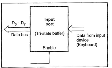
It is used to read data from the input device such as keyboard. The simplest form of input port is a buffer. The input device is connected to the microprocessor through buffer as shown in the Figure. This buffer is a tri-state buffer and its output is available only when enable signal is active.
When microprocessor wants to read data from the input device (keyboard), the control signals from the microprocessor activates the buffer by asserting enable input of the buffer. Once the buffer is enabled, data from the input device is available on the data bus. Microprocessor reads this data by initiating read command.
Output Port :
It is used to send data to the output device such as display from the microprocessor. The simplest form of output port is a latch. The output device is connected to the microprocessor through latch as shown in the Figure.
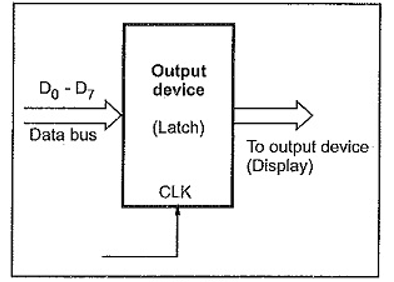
When microprocessor wants to send data to the output device, it puts the data on the data bus and activates the clock signal of the latch, latching the data from the data bus at the output of latch. It is then available at the output of latch for the output device.
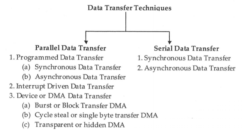
Usually, when memory is connected with the microprocessor, there isn’t a stark difference in the processing speed since semiconductor memories are generally easily compatible with microprocessors. However, this might not always be the case. But the problem often arises when external peripherals are connected as I/O devices. A slow I/O device won’t be able to transfer data at a satisfactory rate whenever the microprocessor requests for data transfer. And usually, the peripheral devices do have slower transfer rates than the processor. Maybe the processor might send two units of information per second, but the external device might only accept 1 unit of information per second. Or conversely, perhaps the external device expects quicker transfers, but our microprocessor might be sending information a bit slower. This might lead to severe data losses, or the devices might get damaged, or there might even be chances for the system to slow down all over, thus affecting the overall efficiency of the system. To avoid this problem, a number of data transfer techniques have been devised.
We can broadly classify the data transfer schemes into two modes – Serial Data Transfer and Parallel Data Transfer.
Xeon processor is a 400 MHz Pentium processor from Intel for use in workstations and enterprise servers. This processor is designed for multimedia applications, engineering graphics, the Internet, and large database servers. The microprocessor history like Xeon includes the following.
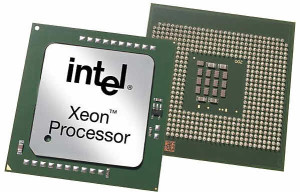
Xeon Processor
The year 2000-2001 marked the introduction of the following processors:
- Jan 12: Intel Pentium III Xeon Processor (800 MegaHertz)
- Sep 25, 2001: Intel Xeon Processor (2 Giga Hertz)
- May 24: Intel Pentium III Xeon Processor (933 MegaHertz)
The year 2002-2004 marked the introduction of the following processors:
- Jan 09, 2002: Intel Xeon Processor (2.20 Giga Hertz)
- March 12, 2002: Intel Xeon Processor M (1.60 Giga Hertz)
- March 10, 2003: Intel Xeon Processor 3 GHz (400 MHz system bus)
- Nov 18: Intel Xeon Processor (2.80 Giga Hertz)
- Oct 6, 2003: Intel Xeon Processor (3.20 Giga Hertz)
- March 2, 2004: Intel Xeon Processor MP 3 GHz (4 MB L3 CACHE)
The year 2005-2008 marked the introduction of the following processors:
- March 2005: Intel Xeon Processor MP (2.666 -3.666 Giga Hertz)
- October 2005: Dual-Core Intel Xeon Processor (2.8 Giga Hertz)
- August 2006: Dual-Core Intel Xeon-7140M (3.33-3.40 Giga Hertz)
The design of such systems requires a general knowledge of the structure of microprocessors, how they are programmed, what kinds of circuitry are needed to put around the basic microprocessor chip to interface to other devices, what other kinds of devices (memories, transmission devices, sensors, controllers, etc.) are used to build systems, and how all of these have to interact with each other in terms of both signals and timing.
Very often microprocessor-based systems are intended as one part of a larger system and not as end products in and of themselves. Such systems are called embedded systems and include things like controllers for automated assembly lines, stop-and-go light controllers for complex intersections, point-of-sale systems, robot controllers or subsystems, and many more. Because of this, it is important to understand not only how to put a microprocessor together with memory but also how to have the system interact with external devices and systems.
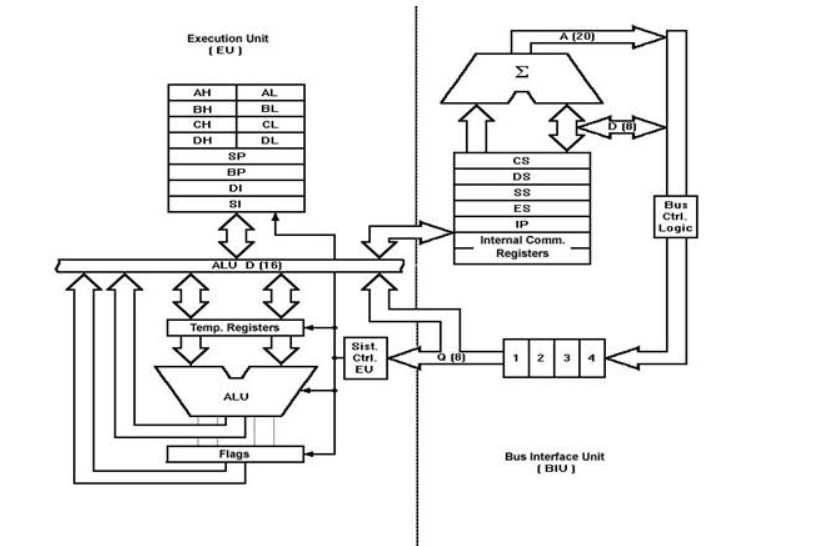
8086, it is a 16-bit Integer processor in a 40 pin, Dual Inline Packaged IC.
The size of the internal registers indicate how much information the processor can operate on at a time and how it moves data around internally within the chip, sometimes also referred to as the internal data bus.
8086 provides the programmer with 14 internal registers, each 16 bits or 2 Bytes wide.
Memory segmentation:
- To increase execution speed and fetching speed, 8086 segments the memory.
- It’s 20 bit address bus can address 1MB of memory, it segments it into 4 64kB segments.
- 8086 works only with four 64KB segments within the whole 1MB memory.
The internal architecture of Intel 8086 is divided into 2 units: The Bus Interface Unit (BIU), and The Execution Unit (EU). These are explained as following below.
The Bus Interface Unit (BIU):
It provides the interface of 8086 to external memory and I/O devices via the System Bus. It performs various machine cycles such as memory read, I/O read etc. to transfer data between memory and I/O devices.
BIU performs the following functions-
- It generates the 20 bit physical address for memory access.
- It fetches instructions from the memory.
- It transfers data to and from the memory and I/O.
- Maintains the 6 byte prefetch instruction queue(supports pipelining).
BIU mainly contains the 4 Segment registers, the Instruction Pointer, a prefetch queue and an Address Generation Circuit.
Instruction Pointer (IP):
- It is a 16 bit register. It holds offset of the next instructions in the Code Segment.
- IP is incremented after every instruction byte is fetched.
- IP gets a new value whenever a branch instruction occurs.
- CS is multiplied by 10H to give the 20 bit physical address of the Code Segment.
- Address of the next instruction is calculated as CS x 10H + IP.
Example:
CS = 4321 H IP = 1000H
Then CS x 10 H = 4321 H + offset = 44210 H
This is the address of the instruction.
Code Segment register:
CS holds the base address for the Code Segment. All programs are stored in the Code Segment and accessed via the IP.
Data Segment register:
DS holds the base address for the Data Segment.
Stack Segment register:
SS holds the base address for the Stack Segment.
Extra Segment register:
ES holds the base address for the Extra Segment.
6 Byte Pre-fetch Queue:
- It is a 6 byte queue (FIFO).
- Fetching the next instruction (by BIU from CS) while executing the current instruction is called pipelining.
- Gets flushed whenever a branch instruction occurs.
The Execution Unit (EU):
The main components of the EU are General purpose registers, the ALU, Special purpose registers, Instruction Register and Instruction Decoder and the Flag/Status Register.
- Fetches instructions from the Queue in BIU, decodes and executes arithmetic and logic operations using the ALU.
- Sends control signals for internal data transfer operations within the microprocessor.
- Sends request signals to the BIU to access the external module.
- It operates with respect to T-states (clock cycles) and not machine cycles.
It has four general purpose registers AX, BX, CX and DX. Store intermediate values during execution. Each of these have two 8 bit parts (higher and lower).
- AX register:
It holds operands and results during multiplication and division operations. Also an accumulator during String operations.
- BX register:
It holds the memory address (offset address) in indirect addressing modes.
- CX register:
It holds count for instructions like loop, rotate, shift and string operations.
- DX register:
It is used with AX to hold 32 bit values during multiplication and division.
Arithmetic Logic Unit (16 bit):
Performs 8 and 16 bit arithmetic and logic operations.
Special purpose registers (16-bit):
- Stack Pointer:
Points to Stack top. Stack is in Stack Segment, used during instructions like PUSH, POP, CALL, RET etc.
- Base Pointer:
BP can hold offset address of any location in the stack segment. It is used to access random locations of the stack.
- Source Index:
It holds offset address in Data Segment during string operations.
- Destination Index:
It holds offset address in Extra Segment during string operations.
Instruction Register and Instruction Decoder:
The EU fetches an opcode from the queue into the instruction register. The instruction decoder decodes it and sends the information to the control circuit for execution.
Flag/Status Registers
It has 9 flags that help change or recognize the state of the microprocessor.
6 Status flags:
- Carry flag(CF)
- Parity flag(PF)
- Auxiliary carry flag(AF)
- Zero flag(Z)
- Sign flag(S)
- Overflow flag (O)
Status flags are updated after every arithmetic and logic operation.
3 Control flags:
- Trap flag(TF)
- Interrupt flag(IF)
- Direction flag(DF)
These flags can be set or reset using control instructions like CLC, STC, CLD, STD, CLI, STI, etc.
The Control flags are used to control certain operations.
The bus interface unit provides the interface of 8086 to external memory and I/O devices via the System Bus. It performs various machine cycles such as memory read, I/O read etc. to transfer data between memory and I/O devices.
BIU performs the following functions-
- It generates the 20 bit physical address for memory access.
- It fetches instructions from the memory.
- It transfers data to and from the memory and I/O.
- Maintains the 6 byte prefetch instruction queue(supports pipelining).
- The BIU has a Physical Address Generation Circuit.
- It generates the 20 bit physical address using Segment and Offset addresses using the formula:
- Physical Address
= Segment Address x 10H + Offset Address
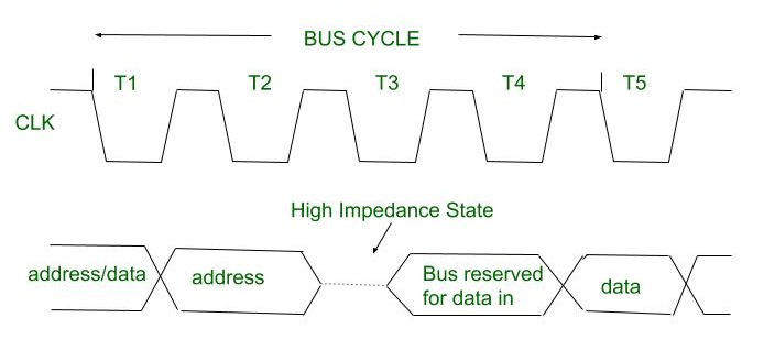
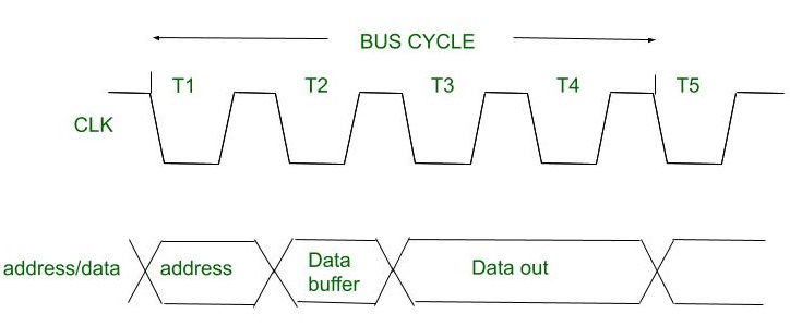
There are at least four clock periods in a bus cycle of 8086 microprocessor. These four clock periods are called T1, T2, T3 and T4 states.
These four clock states gives bus cycle duration T of 200 ns *4 = 800 ns in 5-MHz 8086 system.
- Read Cycle :
When a read cycle is to be performed, during T1 microprocessor puts an address on address bus, and then bus is put in high impedance state during T2 state. Data to be read must be out on bus during T3 and T4. During T3 bus is made “reserved for data in” and finally data is read during T4.
- Write Cycle :
In case of write memory cycle, during T1 state microprocessor puts an address on address bus. Data is put on data bus by CPU during T2 state and maintained during T3 and T4 states, that is written out to memory or I/O devices.
The important Companion chips are:
- Clock Generator Intel 8284
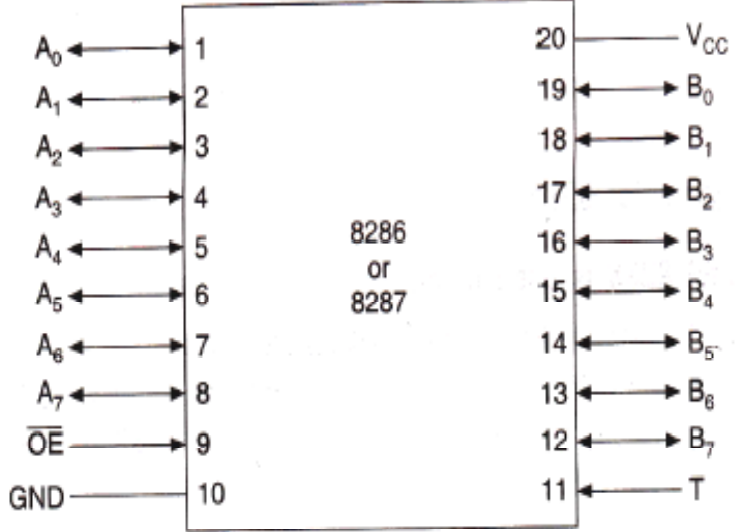
- Bidirectional Bus Transceiver Intel 8286/8287
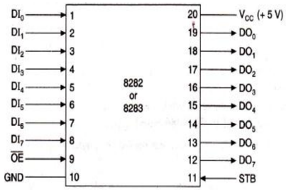
- 8 Bit Input/Output Port Intel S282/8283
- Bus Controller Intel 8288
Clock Generator
Bidirectional Bus Transceiver Intel 8286/8287
S282/8283
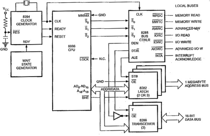
A processor is in the Maximum Mode Configuration of 8086 when its MN/MX pin is grounded. The maximum mode defines pins 24 to 31 as follows:
Pin Definitions (24 to 31) in Maximum Mode:
QS1, QS0 (output) : These two output signals reflect the status of the instruction queue. This status indicates the activity in the queue during the previous clock cycle.
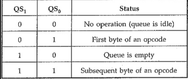
S2,S1,S0 (output) : These three status signals indicate the type of transfer to be take place during the current bus cycle.

LOCK : This signal indicates that an instruction with a LOCK prefix is being executed and the bus is not to be used by another processor:
RQ/GT1 and RQ/GT0 : In the Maximum Mode Configuration of 8086, HOLD and HLDA pins are replaced by RQ (Bus request)/GT0 (Bus Grant), and RQ/GT1 signals. By using bus request signal another master, can request for the system bus and processor communicate.that the request is granted to the requesting master by using bus grantnal. Both signals are similar except the RQ/GT0 has higher priority than RQ/GT1.
Figure shows the typical Maximum Mode Configuration of 8086. In the maximum mode additional circuitry is required to translate the control signals. The additional circuitry converts the status signals (S2-S0) into the I/O and memory transfer signals. It also generates the control signals required to direct the data flow and for controlling 8282 latches and 8286 transceivers. The Intel 8288 bus controller is used to implement this control circuitry.
There are four common types of memory:
• Read only memory ( ROM )
• Flash memory ( EEPROM )
• Static Random access memory ( SARAM )
• Dynamic Random access memory ( DRAM ).
• Pin connections common to all memory devices are:
The address input, data output or input/outputs, selection input and control input used to select a read or write operation.
• Address connections: All memory devices have address inputs that select a memory location within the memory device. Address inputs are labeled from A0 to An.
• Data connections: All memory devices have a set of data outputs or input/outputs. Today many of them have bi-directional common I/O pins.
• Selection connections: Each memory device has an input, that selects or enables the memory device. This kind of input is most often called a chip select ( CS ), chip enable ( CE ) or simply select ( S ) input.
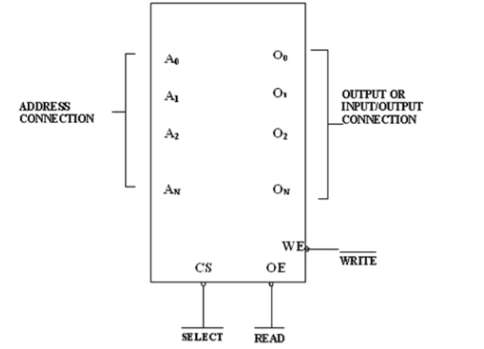
RAM memory generally has at least one CS or S input and ROM at least one CE . • If the CE , CS , S input is active the memory device perform the read or write. • If it is inactive the memory device cannot perform read or write operation. • If more than one CS connection is present, all are active to perform read or write data.
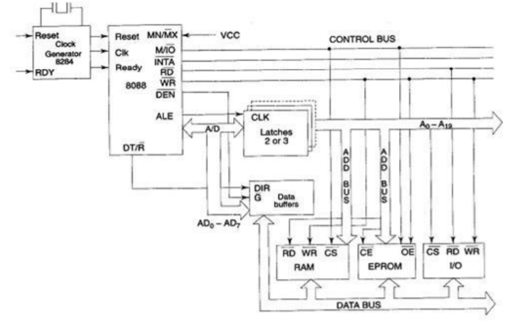
•In a minimum mode 8086 system, the microprocessor 8086 is operated in minimum mode by strapping its MN/MX pin to logic 1.
•In this mode, all the control signals are given out by the microprocessor chip itself. There is a single microprocessor in the minimum mode system.
•The remaining components in the system are latches, transreceivers, clock generator, memory and I/O devices. Some type of chip selection logic may be required for selecting memory or I/O devices, depending upon the address map of the system.
•Latches are generally buffered output D-type flip-flops like 74LS373 or 8282. They are used for separating the valid address from the multiplexed address/data signals and are controlled by the ALE signal generated by 8086.
•Transreceivers are the bidirectional buffers and sometimes they are called as data amplifiers. They are required to separate the valid data from the time multiplexed address/data signals.
•They are controlled by two signals namely, DEN and DT/R. •The DEN signal indicates the direction of data, i.e. from or to the processor. The system contains memory for the monitor and users program storage.
•Usually, EPROMs are used for monitor storage, while RAM for users program storage. A system may contain I/O devices.
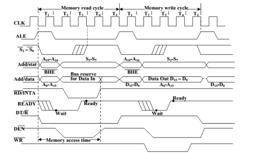
•The opcode fetch and read cycles are similar. Hence the timing diagram can be categorized in two parts, the first is the timing diagram for read cycle and the second is the timing diagram for write cycle.
•The read cycle begins in T1 with the assertion of address latch enable (ALE) signal and also M / IO signal. During the negative going edge of this signal, the valid address is latched on the local bus.
•The BHE and A0 signals address low, high or both bytes. From T1 to T4, the M/IO signal indicates a memory or I/O operation.
•At T2, the address is removed from the local bus and is sent to the output. The bus is then tristated. The read (RD) control signal is also activated in T2.
•The read (RD) signal causes the address device to enable its data bus drivers. After RD goes low, the valid data is available on the data bus.
•The addressed device will drive the READY line high. When the processor returns the read signal to high level, the addressed device will again tristate its bus drivers.
•A write cycle also begins with the assertion of ALE and the emission of the address. The M/IO signal is again asserted to indicate a memory or I/O operation. In T2, after sending the address in T1, the processor sends the data to be written to the addressed location.
•The data remains on the bus until middle of T4 state. The WR becomes active at the beginning of T2 (unlike RD is somewhat delayed in T2 to provide time for floating).
•The BHE and A0 signals are used to select the proper byte or bytes of memory or I/O word to be read or write.
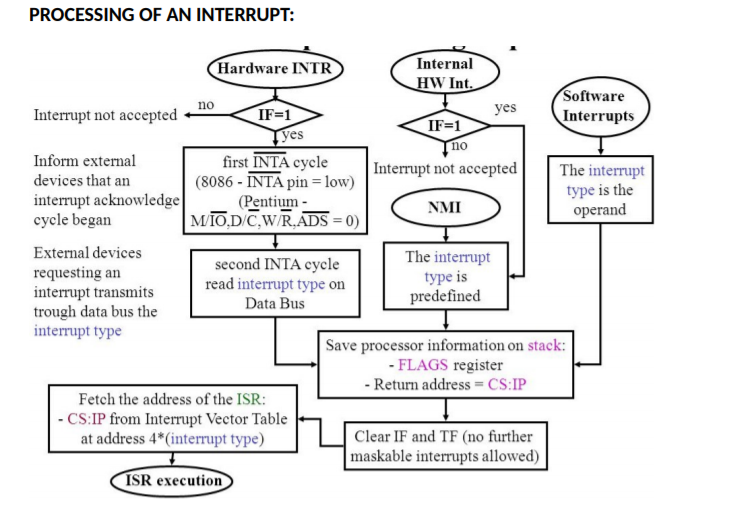
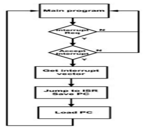
When an interrupt occurs (shown in figure 1), regardless of source, the 80x86 does the following:
1. The CPU pushes the flags register onto the stack.
2. The CPU pushes a far return address (segment: offset) onto the stack, segment value first.
3. The CPU determines the cause of the interrupt (i.e., the interrupt number) and fetches the four byte interrupt vector from address 0: vector*4.
4. The CPU transfers control to the routine specified by the interrupt vector table entry.
References:
1. Microprocessor Book by A.P.Godse and D.A.Godse
2. Microprocessor And Microcontroller Book by A.P.Godse