Unit - 3
Principle of Operation as an amplifier at high frequency
A bipolar junction transistor operated in the microwave region is called a microwave BJT. The operation of the microwave BJT is similar to that of low-frequency transistors. However, the major differences are
• GaAs is to be used instead of silicon, because the mobility of electrons is more in GaAs than in Si.
• To minimize junction capacitance, the size of the device should be minimized.
• The emitter forward resistance is to be minimized by reducing the thickness of the emitter and also by applying maximum possible forward voltage at the emitter junction.
• The base transit time is to be reduced by minimizing its thickness and using a graded doping profile.
In the analysis and designing of a circuit with microwave BJT, the following points should be
considered:
A much more complex equivalent circuit model as shown in the figure below is considered. This includes package parasitic capacitance, lead inductance, and resistance.
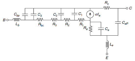
Fig 1 Equivalent circuit of microwave BJT
Cbp —base bond pad capacitance
Cep —emitter bond pad capacitance
Rbc —base contact resistance
Rec —emitter contact resistance
R1, R2, R3 —base distributed resistance
C1, C2, C3 —collector base distributed capacitance
Re —dynamic emitter-base diode resistance
Ce —emitter-base diode junction capacitance
Rc —collector resistance
Lb, Le — base and emitter bond wire inductances
Construction: These are usually N-P-N type, because the electron mobility is higher than the hole mobility. The structure of a conventional Si homojunction N-P-N BJT is as shown in the figure below. N-P-N BJT is designed with planar shape as a double diffused epitaxial transistor.
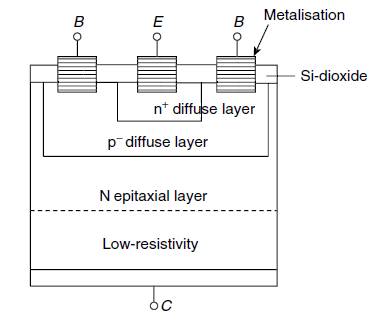
Fig 2 Construction of Microwave BJT
An N-type epitaxial layer, which acts as a collector, is grown on an N + substrate. An insulating layer of silicon dioxide is grown thermally over the epitaxial layer. The base and emitter layer are formed by diffusion or ion implantation. Proper care is to be taken during the whole process of microwave BJT fabrication so as to reduce package parasites considerably. Contacts are provided by means of openings in the oxide, and connections are made in parallel. The surface geometry of the microwave transistor can be any one of the following:
(a) inter-digitized
(b) overlay
(c) matrix
All the three types are as shown in the figure below. In an inter-digitized geometry, a large number of metallized emitter strips alternating with metallized base strips are present as shown in the figure.
This type is used for small signal and power transistors. The second one is the overlay geometry that has a large number of segmented emitters overlying a number of wide metal strips. The third is the matrix or mesh geometry that has an emitter which forms the grid, with the base filling the meshes of this grid with a P+ contact area in the middle of each mesh. Overlay and matrix structures are useful for power transistors.
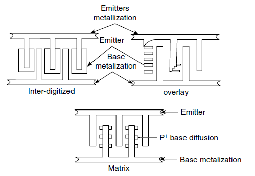
Fig 3 The surface geometry of the microwave transistor
Operation of BJT: Microwave BJT behave very similarly to a low-frequency N-P-N bipolar transistor.
In an N-P-N BJT, primarily, the collector-base and emitter-base junctions are reverse biased, consequent to the class C condition. The microwave frequency signal is applied between the emitter and base junction, this junction forward bias during the positive portion of the microwave signal. A pulse of current flows through the load connected in the collector circuit. In a proper-designed microwave BJT, the emitter current consists almost all of the electrons and is approximately equal to the collector current, while very small fraction of the emitter current is the base current.
The mode mentioned just now is known as an active mode. There are two other operation modes.
One is the cut-off mode, in which the emitter and collector junctions are reverse biased and the collector current is negligible, and another mode is the saturation mode, in which both the emitter and collector junctions are forward biased, resulting in a large collector current.
Disadvantages: Microwave transistors also suffer from high-frequency limitations. The effects like transit time, inter electrode capacitance etc, come into view again at high frequencies. For example, due to the effect of the inter electrode capacitance high frequency response is limited which causes increase the complexity of the transistor. Lead inductance cause undesirable effect. Ideally, these effects should be kept lowest with appropriate selection of geometry and packaging of BJTs. In addition, they operate at lower frequencies than microwave field effect transistors (FETs).
Key takeaway
An N-type epitaxial layer, which acts as a collector, is grown on an N + substrate. An insulating layer of silicon dioxide is grown thermally over the epitaxial layer. The base and emitter layer are formed by diffusion or ion implantation.
It is called as High Electron Mobility Transistor. In addition to the very high frequency performance, the HEMT also offers a very attractive low noise performance. The key element within a HEMT is the specialised PN junction that it uses. It is known as a hetero-junction and consists of a junction that uses different materials either side of the junction. The most common materials used aluminium gallium arsenide (AlGaAs) and gallium arsenide (GaAs).
Structure
Gallium arsenide is generally used because it provides a high level of basic electron mobility which is crucial to the operation of the device. Silicon is not used because it has a much lower level of electron mobility. There is a variety of different structures that can be used within a HEMT, but all use basically the same manufacturing processes. In the manufacture of a HEMT, first an intrinsic layer of gallium arsenide is set down on the semi-insulating gallium arsenide layer. This is only about one micron thick.
Next a very thin layer (between 30 and 60 Angstroms) of intrinsic aluminium gallium arsenide is set down on top of this. Its purpose is to ensure the separation of the hetero-junction interface from the doped aluminium gallium arsenide region. This is critical if the high electron mobility is to be achieved.
The doped layer of aluminium gallium arsenide about 500 Angstroms thick is set down above this. Precise control of the thickness of this layer is required and special techniques are required for the control of this.
There are two main structures that are used. These are the self-aligned ion implanted structure and the recess gate structure. In the case of the self-aligned ion implanted structure the gate, drain and source are set down and are generally metallic contacts, although source and drain contacts may sometimes be made from germanium. The gate is generally made from titanium, and it forms a minute reverse biased junction similar to that of the GaAsFET.
For the recess gate structure another layer of n-type gallium arsenide is set down to enable the drain and source contacts to be made. Areas are etched as shown in the diagram. The thickness under the gate is also very critical since the threshold voltage of the FET is determined by this. The size of the gate, and hence the channel is very small. Typically, the gate is only 0.25 microns or less, enabling the device to have a very good high frequency performance.
Operations
The operation of the HEMT is somewhat different to other types of FET.
Electrons from the n-type region move through the crystal lattice and many remain close to the hetero-junction. These electrons form a layer that is only one electron thick forming what is known as a two-dimensional electron gas. Within this region the electrons are able to move freely because there are no other donor electrons or other items with which electrons will collide and the mobility of the electrons in the gas is very high.
A bias applied to the gate formed as a Schottky barrier diode is used to modulate the number of electrons in the channel formed from the 2 D electron gas and in turn this controls the conductivity of the device. This can be compared to the more traditional types of FET where the width of the channel is changed by the gate bias.
There are several advantages to using HEMT devices:
High gain: HEMTs have a high gain at microwave frequencies because the charge carriers are almost exclusively the majority carriers and the minority carriers are not significantly involved.
Low noise: HEMTs provide very low noise operation because the current variation in the devices is low when compared to other field effect devices.
Key takeaway
It has high speed of operations. It is used in low noise small signal amplifiers, power amplifiers, oscillators and mixers. It is used in RF design applications including cellular telecommunications, DBS radar, radio astronomy.
The Doherty amplifier offers improved efficiency compared to balanced amplifiers, when output power is backed off from saturation. Doherty amplifiers are typically used in communications. The heart of the Doherty amplifier is the Doherty combiner, shown below.
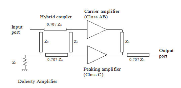
Fig 4 Block Diagram of Doherty Amplifier
This another image of a Doherty amp, which provides an additional degree of freedom.

Fig 5 Doherty Amplifier
The Doherty amplifier power-combines two amplifiers, one is called the "carrier" amplifier while the second is called the "peaking" amplifier. In many Doherty amplifiers the two amplifiers are biased differently, the carrier amp is at a normal Class AB (provides gain at any power level) or Class B, while the peaking amplifier is at Class C which only conducts at half of the cycle. The beauty of the Doherty amplifier is improved power-added efficiency, compared to a balanced amplifier, at backed off power levels.
The Doherty amplifier pair works as follows: on the input the signal is split using a quadrature coupler such as a Lange or branch line hybrid. The input behaves the same as a balanced amplifier, and has the same feature where mismatched amplifiers will have their reflection coefficients reduced if the reflection coefficients are equal in amplitude and phase, the reflected waves end up in the load terminating the isolated port of the coupler.
The output of the Doherty pair is where life gets interesting. The two signals are out of phase by 90 degrees, but by the addition of a quarter-wave transmission line of the peaking amplifier, they are brought back into phase and reactively combined. At this point the two signals in parallel create a Z0/2 impedance.
This is stepped up to Z0 by a quarter-wave transformer. In a fifty-ohm system the transformer would be 35.35 ohms. However, the amplifiers are operating nonlinearly, so the output combiner is more complicated. During operation, the response of one amplifier actively load-pulls the other, as they are not isolated like they would be in a Wilkinson power divider, for example. To design a Doherty amplifier, you are going to need to perform nonlinear analyses.
Key takeaway
The Doherty amplifier pair works as follows: on the input the signal is split using a quadrature coupler such as a Lange or branch line hybrid. The input behaves the same as a balanced amplifier, and has the same feature where mismatched amplifiers will have their reflection coefficients reduced if the reflection coefficients are equal in amplitude and phase, the reflected waves end up in the load terminating the isolated port of the coupler.
Gunn diode has a negative resistance property. To make this negative resistance diode act as an oscillator, it is required is to tune out the capacitance and a shunt load resistance not greater than negative resistance. The efficiency of Gunn diode is only a few percent. It has negative resistance of about 100 ohms in parallel with capacitance of 0.6 pF. A commercial Gunn diode will require a 9 V DC bias with an operating current of 950 mA.
Gunn diode is preferably placed in a resonant cavity which improves the efficiency and allows some variation in the operating frequency. If better electrical tuning is required, a Varactor diode is placed in the cavity at the opposite end to Gunn diode. If a sawtooth sweep voltage is applied to the Varactor diode, the Gunn oscillator will be frequency modulated. The Gunn device can be very well operated as a pulsed oscillator by applying the DC bias voltage in the form of a pulse train of short rectangular pulses. If the duty cycle is low enough and very short bias pulses are applied, the peak power output will be limited only by peak current, since the thermal heating of the device will be negligible.
Cavity Gunn diode oscillator can deliver power output of a few watts at 30 to 40 GHz for continuous operation and up to 200 W in pulsed operation. The heat removal from the small chip of Gunn diode is the most difficult part of its operation. Because of excessive heat, its power handling capability is limited. Commercially Gunn diodes are available for frequencies from 4 GHz to about 100 GHz.
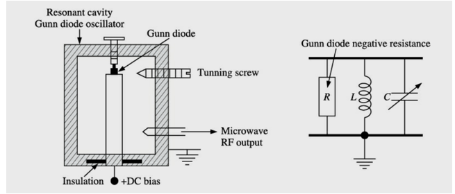
Fig 6 Gunn Diode
Advantages of Gunn Oscillator
Gunn diodes have high frequency stability. They have high reliability and frequency bandwidth. Capable of broad band operation, 2: 1 VSWR for wide bandwidth range. Small size which can be very well located in any part of the circuit. Ruggedness in operation which makes this diode very stable and fit for operation in radars for long duration, deployed in field conditions. Low manufacturing cost. Low supply voltage. Noise performance of Gunn diode is on par with the klystron which is quite acceptable compared to other devices. Gunn diode has huge potential for applications in terahertz frequency band.
Disadvantages of Gunn Diode
Conventional GaAs Gunn Diodes can provide around 500 mW power at 20 GHz with 5.5% efficiency. The efficiency reduces to about 1.5% at 60 GHz and power to 50 mW. It has also been observed that at 77 GHz it gives about 0.8% efficiency. The conventional Gunn diodes have following major limitations: The device has a high turn on voltage. Low efficiency below 10 GHz. The device exhibits poor bias and poor temperature stability. Small tuning range. Spurious FM noise is very high but not bad for normal applications. The device operating current is high thus leading to more power dissipation. At millimeter frequency band, the device has lower efficiency and provides lower power.
Gunn Diode Applications
Because of high frequency capability, Gunn diodes are mainly used at microwave frequencies and above. Some of the important applications are as follows:
Used as low and medium power oscillators in microwave receivers and instruments. Majority of parametric amplifiers use Gunn diode as pump sources. The high-power Gunn oscillators, ranging from 250 to 2000 mW are used as power output oscillators in low power transmitter applications such as police radars, CW Doppler radars etc.
Key takeaway
Gunn diode has a negative resistance property. Gunn diode is preferably placed in a resonant cavity which improves the efficiency and allows some variation in the operating frequency.
The magnetron is a self-contained microwave oscillator that operates differently from linear wave tubes, such as the TWT and Klystron. The magnetrons are cross field tubes in which electric and magnetic fields are perpendicular to each other, so these tubes are known as M-type microwave tubes.
Cylindrical magnetron consists of a cylindrical cathode of finite length and radius 'a' at the centre surrounded by a cylindrical anode of radius 'b'. The anode has several re-entrant cavities which are equi-spaced around the circumference. These cavities are connected between anode and cathode by slots.
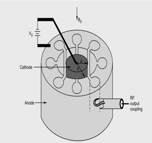
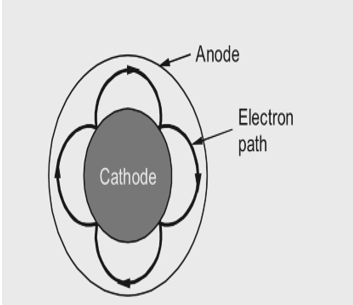
Fig 7 Cylindrical Magnetron
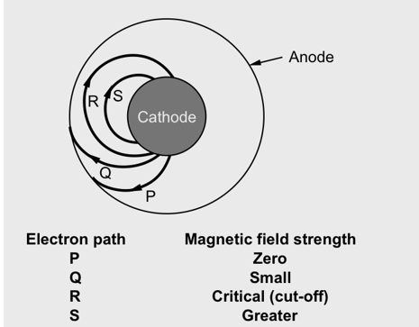
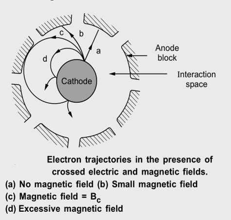
The dc voltage is applied between anode and cathode. The magnetic flux density is maintained in positive-z direction by an electromagnet. If the dc voltage and the magnetic flux are adjusted properly then under the combined forces the electrons follow the cycloidal path between anode-cathode space. The figure below shows the cycloidal path of electrons under the balanced electric and magnetic field strength. The path of electron for various magnetic field strength are shown: The open space between cathode and anode is called the interaction space. In this space, the electric and magnetic fields interact to exert force upon the electrons. The magnetic field is usually provided by a strong permanent magnet mounted around the magnetron so that magnetic field is parallel with the axis of the cathode.
There are three types of Magnetrons
1) Negative resistance type
2) Cyclotron frequency type
3) Travelling wave or cavity type.
1. Negative Resistance Type: These are useful only at the frequency less than 500 MHz. These magnetrons use the negative resistance between two anode segments. The negative resistance magnetrons are capable of generating high power output. The length of the tube plate is limited to few centimetres. The small diameter tube is required to make the magnetron operate efficiently at microwave frequency.
2. Cyclotron Frequency Type: These are useful only for frequencies greater than 100 MHz. The working of these magnetrons depends upon the synchronisation between an alternating component of electric field and periodic oscillations of electrons in the direction parallel to this field.
3. Travelling Wave or Cavity Type: These magnetrons provide the oscillations of very high peak power. These are very useful in radar applications. The working of these magnetrons depends upon the interaction of electrons with a rotating electromagnetic field of constant angular velocity. We have already discussed the construction of these magnetrons. In next section we will discuss the operation of cavity magnetrons.
Working of Magnetron:
1) When there is no RF field in cavity magnetron (zero-mode):
The strong electric field going from anode to cathode is created by applying the negative voltage pulse to cathode. The strong electric field causes the electrons to accelerate towards the anode after they have been accelerated by the cathode. The electron takes the energy from field when it is accelerated by electric field and moves against the electric field. An electron gives up energy to the field and slows down if it moves in the same direction as the electric field.
Oscillations are sustained in the magnetron because of the acceleration and retardation of the electric and magnetic fields. In the diagram a, b c and d are four different electrons which exerts different electric and magnetic field (B = 0), the electron travels in a straight line from cathode to anode due to the radial electric field force action on it. If the magnetic field strength is increased slightly, it will exert lateral force on it and it travels from cathode to anode in a small current path (electron 'b'). As shown in the figure, the radius of the path varies directly with electron velocity and inversely proportional to the magnetic field strength. The radius is given by, R = mV/eB where ‘m’ is mass of the electron, ‘e’ is charge on the electron. When magnetic field is increased, then the electron does not reach the anode shown by path of electron 'C' in the figure and the anode current becomes zero. The magnetic field required to return electrons back to the cathode is called the critical magnetic field. If the magnetic field is made larger than the critical field the electron exerts a greater force on it and it returns back to cathode faster than the electron C, as shown by path of electron 'd' in the figure. All such electrons may cause back heating of the cathode. This can be avoided by switching off the heater.
Fig 8 Electron trajectories in the presence of crossed electric and magnetic fields
2) When the RF oscillations are present in cavity magnetron (-mode):
The RF oscillations are initiated due to some noise transient within the magnetron and oscillations are sustained by the device operation. When n = 4 then there is-mode of operation which is shown in Figure below. The anode poles are-radians apart in phase. The electron ‘a’ is seen to be slowed down in the presence of oscillations thus transferring energy from cathode to anode. The electrons which participate in transferring the energy to the RF field are called forward electrons and they are responsible for the bunching effect.
The electron ' b' is accelerated by the RF field and it takes energy from the oscillations resulting in increased velocity. It bends more sharply, spends very little time in the interaction space and return back to the cathode, these electrons do not participate in the bunching process. The electron 'd' is slowed down and it falls back in step with electron ‘a’.
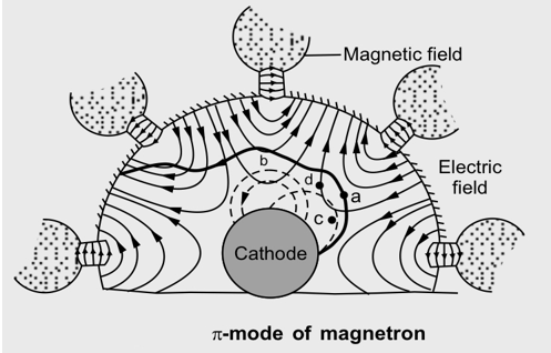
This results in forward electrons like a, c, d to be confined to spokes or electron clouds. The spokes so formed in-mode rotate with an angular velocity corresponding to two poles per cycle. The process is called phase focusing effect, corresponding to a bunch of forward electrons around the reference electron ‘a’. The phase focusing effect of these forward electrons, imparts enough energy to the RF oscillations so that they are sustained.
Strapping
Due to mutual coupling, two or more identical cavities resonate at two different frequencies. The process of separating the - mode from other adjacent mode is known as strapping.
The strapping is also used to avoid the mode jumping in magnetrons. The resonant modes of magnetron are very close to each other. The weaker modes have slightly different frequency from dominant mode so there is always a possibility of mode jumping because the purity of oscillations is lost due to small difference of frequency of oscillations.
The disadvantage of strapping is that it may cause power loss in conducting rings, also at higher frequencies, it may cause power loss in conducting rings. At higher frequencies, it is very difficult to maintain the RF field within the interaction space and strapping causes the stray effects.
Frequency Pushing and Pulling
The process of change in resonant frequency of magnetron by changing the anode voltage is known as the frequency pushing. If there is a change in anode voltage, then orbital velocity of electrons will also change. Due to the change in velocity of electrons, the energy which is transferred to anode resonators is also changed and this factor results in the change of oscillation of frequency.
In magnetron, the change in load impedance causes the variations in frequency. This takes place whether these load variations are purely resistive or reactive variations. The frequency variations due to the change in load impedances are known as the frequency pulling. To minimize the frequency variations a stabilized power supply is used.
To minimize the frequency pushing a circulator is placed before the waveguide connection at the output at the magnetron, this circulator does not allow the backward flow of energy.
Characteristics of Magnetron
The performance characteristics of magnetron is as follows:
2. Power output: 800 kW (pulsed)
3. Operating frequency: up to 10 GHz.
Key takeaway
2. In satellite and missiles for telemetry.
3. Industrial heating.
4. Microwave ovens
A mixer is a three-port component, which performs the task of frequency conversion. Mixers translate the frequency of an input signal to a different frequency. This functionality is vital for a wide range of applications, including military radar, satellite-communications (satcom), cellular base stations, and more. Mixers are used to perform both frequency upconversion and downconversion.
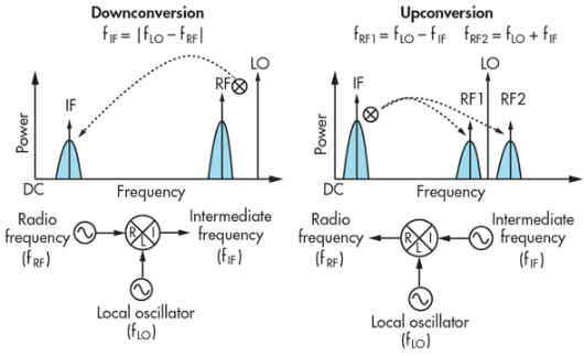
Fig 9 Down and Up Conversion
An ideal mixer produces an output that consists of the sum and difference frequencies of its two input signals. In other words:
fout = fin1 ± fin2
The three ports of a mixer are known as the intermediate-frequency (IF), radio-frequency (RF), and local-oscillator (LO) ports. The LO port is usually an input port.
The RF and IF ports can be used interchangeably, depending on whether the mixer is being used to perform upconversion or downconversion. The LO signal is typically the strongest signal injected into a mixer. The required LO drive level is dependent on several factors, including the mixer’s configuration and device technology.
When a mixer is used to perform downconversion, an input signal enters the RF port and an LO signal enters the LO port. These two input signals produce an output signal at the IF port. The frequency of this output signal is equal to the difference of the RF input signal’s frequency and the LO signal’s frequency.
When a mixer is used to perform upconversion, an input signal enters the IF port and an LO signal enters the LO port. These two input signals produce an output signal at the RF port. The frequency of this output signal is equal to the sum of the IF input signal’s frequency and the LO signal’s frequency. Both downconversion and upconversion are shown graphically in figure above. Upconversion is normally part of a transmitter, while down conversion is typically used in a receiver.
Mixer Parameters
Conversion Loss: In passive mixers, conversion loss is defined as the difference in signal level between the amplitude of the input signal and the amplitude of the desired output signal. In a mixer used for downconversion, the conversion loss is the difference between the RF input signal’s amplitude and the IF output signal’s amplitude. In a mixer used for upconversion, the conversion loss is the difference between the IF input signal’s amplitude and the RF output signal’s amplitude.
Conversion loss is expressed as a positive number in decibels. Typical values of conversion loss can range from approximately 4.5 to 9 dB, depending on the mixer. Conversion loss values of 6 to 8 dB are common in standard double-balanced mixers, while triple-balanced mixers generally have a higher conversion loss than double-balanced mixers. It is also possible to achieve conversion gain in active mixers.
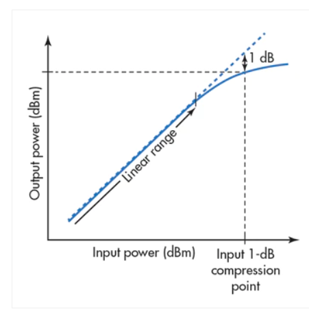
Fig 10 1-dB Compression Point
Isolation is a measurement of the amount of power that leaks from one port to another. Isolation is defined as the difference in signal level between the amplitude of an input signal and the amplitude of the leaked power from that input signal to another port. When isolation is high, the amount of power leaked from one port to a different port is small.
1-dB Compression Point: A mixer’s conversion loss remains constant when the mixer is in linear operation. As the amplitude of the input signal increases, the amplitude of the output signal rises by the same amount. However, once the input signal’s amplitude reaches a certain level, the amplitude of the output signal ceases to exactly follow the input signal. The mixer deviates from linear behaviour and its conversion loss begins to increase.
Intermodulation Distortion: Two-tone third-order intermodulation distortion (IMD) occurs when two signals simultaneously enter the mixer’s IF or RF input port. In practice, this could happen in a multi-carrier signal environment. These two signals interact with each other and with the LO signal, which creates distortion. In a receiver, two-tone third-order IMD is a serious problem because it can generate third-order distortion products that fall within the IF bandwidth.
If fRF1 and fRF2 represent two separate RF input signals and fLO represents the LO signal, the third-order distortion products generated at the mixer’s IF port are:
Interferer1 = 2fRF1 - fRF2 - fLO
Interferer2 = 2fRF2 - fRF1 - fLO
These third-order distortion products are extremely close to the desired IF output frequency. No amount of filtering can remove these unwanted distortion products. Thus, the signal-to-noise ratio of the received signal is degraded, highlighting the need to suppress these distortion products.
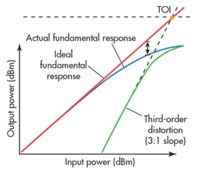
Fig 11 Representation of TOI
The third-order input intercept point (TOI or IP3) is a widely accepted figure of merit used to describe a mixer’s capability to suppress third-order distortion products. TOI is used in predicting the nonlinear behaviour of a mixer as the amplitude of its input signal increases, which causes the third-order products to increase by a 3:1 ratio. For any 1-dB increase in the input signal’s amplitude, the third-order products increase by 3 dB as shown in figure above.
Mixer Design Using Single Diode
Passive mixers primarily use Schottky diodes, although the FET resistive mixer has recently become another popular passive mixer. Active mixers use either FETs or bipolar devices. Schottky diodes, in comparison with FETs and bipolar devices, have the advantage of possessing an inherently wide bandwidth. This is a major reason why diodes are still widely used to design mixers.

Fig 12 Mixer design using Single Diode
Mixers can be designed with just a single diode, which is the simplest mixer topology. Balanced mixers, which consist of two, four, or even eight diodes in a balanced structure, build upon the single-diode mixer. The majority of mixers available today incorporate some form of mixer balancing.
A single diode can be used to create a mixer. Here, the RF and LO signals combine at the anode of the diode. The LO signal needs to be large enough to switch the diode on and off, which causes the actual mixing process. The frequency components generated by single-diode mixers are:
fIF = nfLO ±mfRF (m and n are all integers)
where:
fLO = the LO input signal frequency
fRF = the RF input signal frequency
fIF = the IF output signal frequency
Although only one output frequency is desired (when n = 1 and m = 1), additional unwanted harmonics are generated by the diode’s current-voltage (I-V) characteristics and the transconductance modulation caused by the RF signal. Because the single-diode mixer has no inherent isolation between the RF and LO ports, external filters also are needed to achieve isolation between ports. This need for external filtering makes it difficult to achieve wideband mixers with just a single diode.
Key takeaway
A mixer is a three-port component, which performs the task of frequency conversion. Mixers translate the frequency of an input signal to a different frequency. This functionality is vital for a wide range of applications, including military radar, satellite-communications (satcom), cellular base stations, and more. Mixers are used to perform both frequency upconversion and downconversion.
References:
[1] Microwave Engineering by D. M. Pozor, 2nd Edition. John Willy & Sons. Selected portions from Chapter 2, 3, 4, 6, 7 & 9.
[2] Principles of Microwave Engineering by Reich, Oudong and Others.
[3] Microwave Device and Circuit, 3rd Edition, Sammuel Y., Liao, Perason
[4] Microwave Devices and Circuits, G S N Raju