Unit - 1
Revision of Number System
A digital system understands positional number system where there are few symbols called digits and these symbols represents different values depending on their position in the number.
A value of the digit is determined by using
Decimal Number System
(1×1000) + (2×100) + (3×10) + (4×l)
(1×10³) + (2×10²) + (3×101) + (4×l00)
1000 + 200 + 30 + 1
1234
S.N. | Number System & Description |
1 | Binary Number System Base 2. Digits used: 0 and 1 |
2 | Octal Number System Base 8. Digits used: 0 to 7 |
3 | Hexa Decimal Number System Base 16. Digits used: 0 to 9, Letters used: A- F |
Binary Number System
Example
Binary Number: 101112
Calculating the Decimal Equivalent of binary number −
Step | Binary Number | Decimal Number |
Step 1 | 101012 | ((1 × 24) + (0 × 23) + (1 × 22) + (1 × 21) + (1 × 20))10 |
Step 2 | 101012 | (16 + 0 + 4 + 2 + 1)10 |
Step 3 | 101012 | 2310 |
Note: 101112 is normally written as 10111.
Octal Number System
Example
Octal Number − 125758
Calculating Decimal Equivalent −
Step | Octal Number | Decimal Number |
Step 1 | 125758 | ((1 × 84) + (2 × 83) + (5 × 82) + (7 × 81) + (5 × 80))10 |
Step 2 | 125758 | (4096 + 1024 + 320 + 56 + 5)10 |
Step 3 | 125758 | 550010 |
Note: 125758 is normally written as 12575 in octal.
Hexadecimal Number System
Example −
Hexadecimal Number: 19FDA16
Calculating Decimal Equivalent −
Step | Hexadecimal Number | Decimal Number |
Step 1 | 19FDA16 | ((1 × 164) + (9 × 163) + (F × 162) + (D × 161) + (A × 160))10 |
Step 2 | 19FDA16 | ((1 × 164) + (9 × 163) + (15 × 162) + (13 × 161) + (10 × 160))10 |
Step 3 | 19FDA16 | (65536 + 36864 + 3840 + 208 + 10)10 |
Step 4 | 19FDA16 | 10645810 |
Note − 19FDA16 is normally written as 19FDA in hexa decimal.
Conversions:
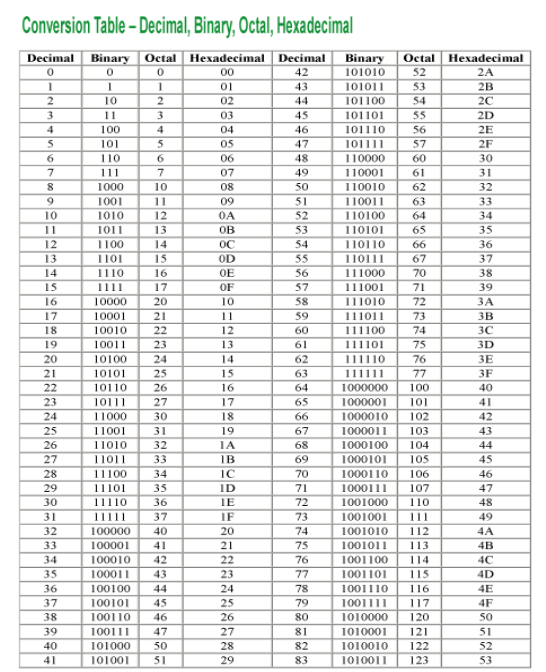
There are many techniques which are used to convert numbers from one base to another. These are as follows −
Decimal to Any Base System
It includes the following steps:
For example −
Decimal Number: 2710
Calculating Binary Equivalent −
Step | Operation | Result | Remainder |
Step 1 | 27 / 2 | 13 | 1 |
Step 2 | 13 / 2 | 6 | 1 |
Step 3 | 6 / 2 | 3 | 0 |
Step 4 | 3 / 2 | 1 | 1 |
Step 5 | 1 / 2 | 0 | 1 |
Hence, the remainders are arranged in the reverse order and we get:
Decimal Number − 2710 = Binary Number − 110112.
Any Base System to Decimal System
For example:
Binary Number − 111102
Calculating Decimal Equivalent −
Step | Binary Number | Decimal Number |
Step 1 | 111102 | ((1 × 24) + (1 × 23) + (1 × 22) + (1 × 21) + (0 × 20))10 |
Step 2 | 111102 | (16 + 8 + 4 + 2 + 0)10 |
Step 3 | 111102 | 3010 |
Binary Number − 111102 = Decimal Number − 3010
Any Base System to Non-Decimal System
Example
Octal Number − 268
Calculating its Binary Equivalent −
Step 1 – Converting octal to Decimal
Step | Octal Number | Decimal Number |
Step 1 | 268 | ((2 × 81) + (6 × 80))10 |
Step 2 | 268 | (16 + 6 )10 |
Step 3 | 268 | 2210 |
Octal Number − 268 = Decimal Number − 2210
Step 2 − Converting Decimal to Binary
Step | Operation | Result | Remainder |
Step 1 | 22 / 2 | 11 | 0 |
Step 2 | 11 / 2 | 5 | 1 |
Step 3 | 5 / 2 | 2 | 1 |
Step 4 | 2 / 2 | 1 | 0 |
Step 5 | 1 / 2 | 0 | 1 |
Decimal Number − 2210 = Binary Number − 101102
Octal Number − 268 = Binary Number − 101102
Binary to Octal
For example:
Binary Number − 101012
Its Octal Equivalent −
Step | Binary Number | Octal Number |
Step 1 | 101012 | 010 101 |
Step 2 | 101012 | 28 58 |
Step 3 | 101012 | 258 |
Binary Number − 101012 = Octal Number − 258
Octal to Binary
For example:
Octal Number − 258
Its Binary Equivalent −
Step | Octal Number | Binary Number |
Step 1 | 258 | 210 510 |
Step 2 | 258 | 0102 1012 |
Step 3 | 258 | 0101012 |
Octal Number − 258 = Binary Number − 101012
Binary to Hexadecimal
For example:
Binary Number − 101012
Its hexadecimal Equivalent −
Step | Binary Number | Hexadecimal Number |
Step 1 | 101012 | 0001 0101 |
Step 2 | 101012 | 110 510 |
Step 3 | 101012 | 1516 |
Binary Number − 101012 = Hexadecimal Number − 1516
Hexadecimal to Binary
For example:
Hexadecimal Number − 1516
Its Binary Equivalent −
Step | Hexadecimal Number | Binary Number |
Step 1 | 1516 | 110 510 |
Step 2 | 1516 | 00012 01012 |
Step 3 | 1516 | 000101012 |
Hexadecimal Number − 1516 = Binary Number − 101012
Key takeaway
Binary system complements:
S.N. | Complement | Description |
1 | Radix Complement | It is referred to as the r's complement. |
2 | Diminished Radix Complement | It is referred to as the (r-1)'s complement. |
1's complement
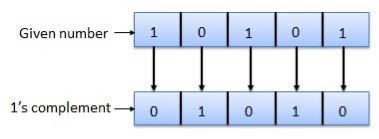
Fig.1: 1's complement
2's complement
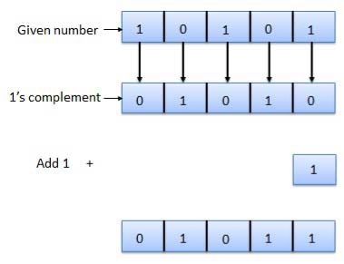
Fig.2: 2's complement
Using 1’s complement:
Example1: Subtract 134 from 168.
Sol: 168-134 = 168 + (-134)
Binary representation of 168= 1010 1000
Binary representation of 134= 1000 0110
Binary representation of -134= 0111 1001
[Because 1’s complement represents the negative magnitude of a binary number]
168 + (-134) = 1010 1000 + 0111 1001 = 10010 0001
As a carry bit is present, 1 will be added to the result and it represents that the result is positive. 0010 0001 + 1 = 0010 0010
Decimal representation of 0010 0010 is 34.
168-134=34; hence the result is correct.
Example2: Subtract 168 from 134.
Sol: 134-168 = 134 + (-168)
Binary representation of 134= 1000 0110
Binary representation of 168= 1010 1000
Binary representation of -168= 0101 0111
[Because 1’s complement represents the negative magnitude of a binary number]
134 + (-168) = 1000 0110 + 0101 0111=1101 1101
As a carry bit is absent, 1’s complement of this value will be the final result and absence of carry bit represents that the result is negative.
1’s complement of 1101 1101 = 0010 0010
Decimal representation of 0010 0010 is 34.
As carry bit is absent the result is negative i.e., -34 134 -168= -34; hence the result is correct.
Using 2’s complement
Example 1: Subtract 96 from 118.
Sol: 118-96 = 118 + (-96)
Binary representation of 118= 0111 0110
Binary representation of 96= 0110 0000
Here 2’s complement represents the negative magnitude of a binary number.
Hence 2’s complement of 96 represents -96.
So -96= 1001 1111 118 + (-96) = 0111 0110 + 1001 1111=10001 0101
As a carry bit is present, 1 will be added to the result and presents of carry bit represents that the result is positive. 0001 0101+ 1= 0001 0110
Decimal representation of 0001 0110 is 22.
As carry bit is present the result is positive.
Example 2: Subtract 118 from 96.
Sol: 118-96 = 96 + (-118)
Binary representation of 96= 0110 0000
Binary representation of 118= 0111 0110
Here 2’s complement represents the negative magnitude of a binary number.
Hence 2’s complement of 118 represents -118.
So -118= 1000 1010 96 + (-118) = 0110 0000 + 1000 1010 1110 1010
As a carry bit is absent, 2’s complement of this value will be the final result and absence of carry bit represents that the result is negative.
2’s complement of 1110 1010 = 0001 0110
Decimal representation of 0001 0110 is 34. As carry bit is absent the result is negative i.e., -34
Key takeaway
2's complement
Signed Binary:
 For a binary number the most significant bit (MSB) denotes the signed bit. For example, +9 using 8-bits is denoted as 10001001
MSB
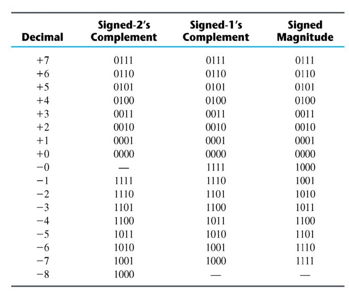
The table below shows all the signed four-bit binary numbers.
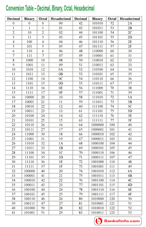
Binary Addition
Binary Addition in 2’s compliment form:
Binary Subtraction in 2’s compliment form:
For example: (-6) -(-13) = (11111010 – 11110011)
= (11111010+00001101)
= (00000111) = +7
Floating Point Numbers
This is the most common method for representation of real numbers on computers. To represent floating point numbers IEEE has set a standard. IEEE 754 numbers have basic components as listed below:
We can summarise the above as:
The exponent base is two. The exponent field contains 127 plus the true exponent for single-precision, or 1023 plus the true exponent for double precision. The first bit of the mantissa is typically assumed to be 1.
On the basis of above three components IEEE 754 can be categorised as
a) Single Precision: It is 8-bit exponent field.

The number ranges which the single precision floating point number cannot represent are:
i) Negative numbers less than −(2−2−23) × 2127
ii) Negative numbers greater than −2−149
iii) Zero
iv) Positive numbers less than 2−149
v) Positive numbers greater than (2−2−23) × 2127
b) Double Precision

Few numbers which are still not defined in this standard are:
i) Denormalized: If the exponent is 0 the value is a denormalized number.
Key takeaway
The exponent field contains 127 plus the true exponent for single-precision, or 1023 plus the true exponent for double precision. The first bit of the mantissa is typically assumed to be 1.
Advantages of Binary Code
Classification of binary codes
The codes are broadly classified as:
Weighted Codes
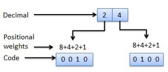
Fig.3: Weighted codes (Ref. 1)
Non-Weighted Codes
1.Excess-3 code

Example
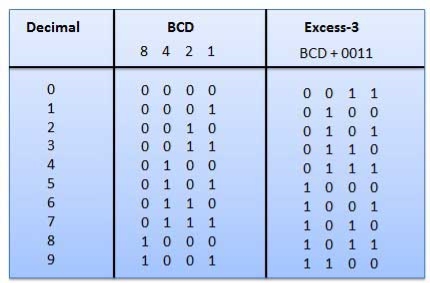
Fig.4: BCD to XS 3 conversion (Ref. 1)
2.Gray Code
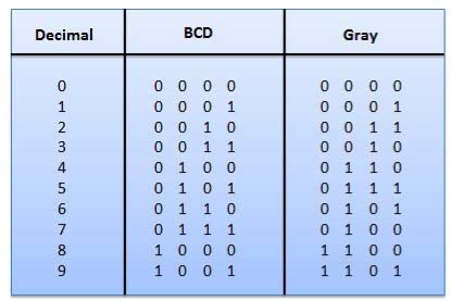
Fig.5: Gray codes (Ref. 1)
Application of Gray code
3. Binary Coded Decimal (BCD) code

Fig.6: BCD codes (Ref. 1)
Advantages of BCD Codes
Disadvantages of BCD Codes
4. Alphanumeric codes
5.Error Codes
There technique is available to detect and correct data during data transmission.
Error Code | Description |
Error Detection and Correction | Error detection and correction code techniques |
Key takeaway
In BCD code only first ten of these numbers are used (0000 to 1001) and rest are invalid.
ASCII code is a 7-bit code whereas EBCDIC is an 8-bit code.
Postulates and Basic Laws of Boolean Algebra
Here, the Boolean postulates and basic laws that are used are given underneath.
Boolean Postulates
x + 0 = x
x + 1 = 1
x + x = x
x + x’ = 1
x.1 = x
x.0 = 0
x.x = x
x.x’ = 0
Basic Laws of Boolean Algebra
Commutative Law
x + y = y + x
x.y = y.x
Associative Law
x + (y + z) = (x + y) + z
x. (y.z) = (x.y). z
Distributive Law
x. (y + z) = x.y + x.z
x + (y.z) = (x + y). (x + z)
Theorems of Boolean Algebra
- Duality theorem
- De Morgan’s theorem
Duality Theorem
Group1 | Group2 |
x + 0 = x | x.1 = x |
x + 1 = 1 | x.0 = 0 |
x + x = x | x.x = x |
x + x’ = 1 | x.x’ = 0 |
x + y = y + x | x.y = y.x |
x + (y + z) = (x + y) + z | x. (y.z) = (x.y). z |
x. (y + z) = x.y + x. z | x + (y.z) = (x + y). (x + z) |
De Morgan’s Theorem
(x + y)’ = x’. y’
(x.y)’ = x’ + y’
Simplification of Boolean Functions
Numerical
f = p’qr + pq’r + pqr’ + pqr
Method 1
Given
f = p’qr + pq’r + pqr’ +pqr.
In first and second term r is common and in third and fourth terms pq is common.
So, taking out the common terms by using Distributive law we get,
⇒ f = (p’q + pq’) r + pq (r’ + r)
The terms present in first parenthesis can be simplified by using Ex-OR operation.
The terms present in second parenthesis is equal to ‘1’ using Boolean postulate we get
⇒ f = (p ⊕q) r + pq (1)
The first term can’t be simplified further.
But, the second term is equal to pq using Boolean postulate.
⇒ f = (p ⊕q) r + pq
Therefore, the simplified Boolean function is f = (p⊕q) r + pq
Method 2
Given f = p’qr + pq’r + pqr’ + pqr.
Using the Boolean postulate, x + x = x.
Hence, we can write the last term pqr two more times.
⇒ f = p’qr + pq’r + pqr’ + pqr + pqr + pqr
Now using the Distributive law for 1st and 4th terms, 2nd and 5th terms, 3rdand 6th terms we get.
⇒ f = qr (p’ + p) + pr (q’ + q) + pq (r’ + r)
Using Boolean postulate, x + x’ = 1 and x.1 = x for further simplification.
⇒ f = qr (1) + pr (1) + pq (1)
⇒ f = qr + pr + pq
⇒ f = pq + qr + pr
Therefore, the simplified Boolean function is f = pq + qr + pr.
Hence, we got two different Boolean functions after simplification of the given Boolean function. Functionally, these two functions are same. As per requirement, we can choose one of them.
Numerical
Find the complement of the Boolean function,
f = p’q + pq’.
Solution:
Using DeMorgan’s theorem, (x + y)’ = x’. y’ we get
⇒ f’ = (p’q)’. (pq’)’
Then by second law, (x.y)’ = x’ + y’ we get
⇒ f’ = {(p’)’ + q’}. {p’ + (q’)’}
Then by using, (x’)’=x we get
⇒ f’ = {p + q’}. {p’ + q}
⇒ f’ = pp’ + pq + p’q’ + qq’
Using x.x’=0 we get
⇒ f = 0 + pq + p’q’ + 0
⇒ f = pq + p’q’
Therefore, the complement of Boolean function, p’q + pq’ is pq + p’q’.
Key takeaways
1.6 Complete Logic set
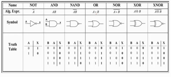
If any digital circuit can be built from a set of gates, that set is said to be functionally complete
The NAND gate is functionally complete
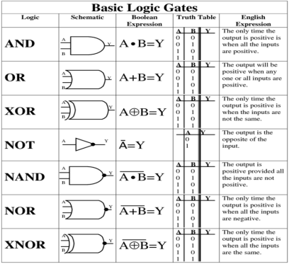
Basic Gates
The basic gates are namely AND gate, OR gate & NOT gate.
AND gate
It is a digital circuit that consists of two or more inputs and a single output which is the logical AND of all those inputs. It is represented with the symbol ‘.’.
The following is the truth table of 2-input AND gate.
A | B | Y = A. B |
0 | 0 | 0 |
0 | 1 | 0 |
1 | 0 | 0 |
1 | 1 | 1 |
Here A, B are the inputs and Y is the output of two input AND gate.
If both inputs are ‘1’, then only the output, Y is ‘1’. For remaining combinations of inputs, the output, Y is ‘0’.
The figure below shows the symbol of an AND gate, which is having two inputs A, B and one output, Y.

Fig.7: AND gate (ref. 1)
OR gate
It is a digital circuit which has two or more inputs and a single output which is the logical OR of all those inputs. It is represented with the symbol ‘+’.
The truth table of 2-input OR gate is:
A | B | Y = A + B |
0 | 0 | 0 |
0 | 1 | 1 |
1 | 0 | 1 |
1 | 1 | 1 |
Here A, B are the inputs and Y is the output of two input OR gate.
When both inputs are ‘0’, then only the output, Y is ‘0’. For remaining combinations of inputs, the output, Y is ‘1’.
The figure below shows the symbol of an OR gate, which is having two inputs A, B and one output, Y.

Fig.8: OR gate (ref. 1)
NOT gate
It is a digital circuit that has one input and one output. Here the output is the logical inversion of input. Hence, it is also called as an inverter.
The truth table of NOT gate is:
A | Y = A’ |
0 | 1 |
1 | 0 |
Here A and Y are the corresponding input and output of NOT gate. When A is ‘0’, then, Y is ‘1’. Similarly, when, A is ‘1’, then, Y is ‘0’.
The figure below shows the symbol of NOT gate, which has one input, A and one output, Y.

Fig.9: NOT gate (ref. 1)
NAND gate
It is a digital circuit which has two or more inputs and single output and it is the inversion of logical AND gate.
The truth table of 2-input NAND gate is:
A | B | Y = (A.B)’ |
0 | 0 | 1 |
0 | 1 | 1 |
1 | 0 | 1 |
1 | 1 | 0 |
Here A, B are the inputs and Y is the output of two input NAND gate. When both inputs are ‘1’, then the output, Y is ‘0’. If at least one of the inputs is zero, then the output, Y is ‘1’. This is just the inverse of AND operation.
The image shows the symbol of NAND gate:

Fig.10: NAND gate (ref. 1)
NAND gate works same as AND gate followed by an inverter.
NOR gate
It is a digital circuit that has two or more inputs and a single output which is the inversion of logical OR of all inputs.
The truth table of 2-input NOR gate is:
A | B | Y = (A+B)’ |
0 | 0 | 1 |
0 | 1 | 0 |
1 | 0 | 0 |
1 | 1 | 0 |
Here A and B are the two inputs and Y is the output. If both inputs are ‘0’, then the output is ‘1’. If any one of the inputs is ‘1’, then the output is ‘0’. This is exactly opposite to two input OR gate operation.
The symbol of NOR gate is:

Fig.11: NAND gate (ref. 1)
NOR gate works exactly same as that of OR gate followed by an inverter.
Special Gates
Ex-OR gate
It stands for Exclusive-OR gate. Its function varies when the inputs have even number of ones.
The truth table of 2-input Ex-OR gate is:
A | B | Y = A⊕B |
0 | 0 | 0 |
0 | 1 | 1 |
1 | 0 | 1 |
1 | 1 | 0 |
Here A, B are the inputs and Y is the output of two input Ex-OR gate. The output (Y) is zero instead of one when both the inputs are one.
Therefore, the output of Ex-OR gate is ‘1’, when only one of the two inputs is ‘1’. And it is zero, when both inputs are same.
The symbol of Ex-OR gate is as follows:

Fig.12: XOR gate (ref. 1)
It is similar to that of OR gate with an exception for few combination(s) of inputs. Hence, the output is also known as an odd function.
Ex-NOR gate
It stands for Exclusive-NOR gate. Its function is same as that of NOR gate except when the inputs having even number of ones.
The truth table of 2-input Ex-NOR gate is:
A | B | Y = A⊙B |
0 | 0 | 1 |
0 | 1 | 0 |
1 | 0 | 0 |
1 | 1 | 1 |
Here A, B are the inputs and Y is the output. It is same as Ex-NOR gate with the only modification in the fourth row. The output is 1 instead of 0, when both the inputs are one.
Hence the output of Ex-NOR gate is ‘1’, when both inputs are same and 0, when both the inputs are different.
The symbol of Ex-NOR gate is:

Fig.13: XNOR gate (ref. 1)
It is similar to NOR gate except for few combination(s) of inputs. Here the output is ‘1’, when even number of 1 is present at the inputs. Hence is also called as an even function.
Key takeaway
1.9 Algebraic Reduction and realization using logic gates
Boolean Expression for a Logic Circuit To derive the Boolean expression for a given logic circuit, begin at the leftmost inputs and work toward the final output, writing the expression for each gate. For the example circuit in Fig, the Boolean expression is determined as follows:
The expression for the left-most AND gate with inputs C and D is CD.
The output of the left-most AND gate is one of the inputs to the OR gate and B is the other input. Therefore, the expression for the OR gate is B + CD.
The output of the OR gate is one of the inputs to the right-most AND gate and A is the other input. Therefore, the expression for this AND gate is A (B + CD), which is the final output expression for the entire circuit.

Fig 14 Logic Circuit showing the Boolean Expression for the output
Examples
Q1) Using Boolean algebra techniques, simplify this expression: AB + A (B + C) + B (B + C)
Solution
Step 1: Apply the distributive law to the second and third terms in the expression, as follows: AB + AB + AC + BB + BC
Step 2: Apply rule 7 (BB = B) to the fourth term. AB + AB + AC + B + BC
Step 3: Apply rule 5 (AB + AB = AB) to the first two terms. AB + AC + B + BC
Step 4: Apply rule 10 (B + BC = B) to the last two terms. AB + AC + B
Step 5: Apply rule 10 (AB + B = B) to the first and third terms. B+AC At this point the expression is simplified as much as possible.
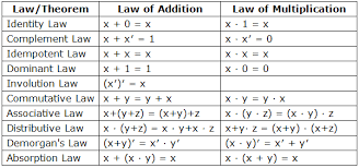
Fig 15 Implementation using gates
Q2) Design a logic circuit that has three inputs, A, B, and C, and whose output will be HIGH only when a majority of the inputs are HIGH.
Solution Step 1. Set up the truth table. On the basis of the problem statement, the output x should be 1 whenever two or more inputs are 1; for all other cases, the output should be 0
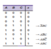
Fig 16 Truth Table with AND terms
Step 2. Write the AND term for each case where the output is a 1. There are four such cases. The AND terms are shown next to the truth table. Again, note that each AND term contains each input variable in either inverted or noninverted form.
Step 3. Write the sum-of-products expression for the output. x =  BC + A
 C + AB
 + ABC
+ ABC
Step 4. Simplify the output expression.
This expression can be simplified in several ways. Perhaps the quickest way is to realize that the last term ABC has two variables in common with each of the other terms. Thus, we can use the ABC term to pair with each of the other terms. The expression is rewritten with the ABC term occurring three times:
x =  BC + A
 C + AB
 + ABC + ABC + ABC
Factoring the appropriate pairs of terms, we have
x = BC ( + A) + AC (
 + B) + AB (
 + C) Each term in parentheses is equal to 1, so we have x = BC + AC + AB
Step 5. Implement the circuit for the final expression. This expression is implemented in Figure. Since the expression is in SOP form, the circuit consists of a group of AND gates working into a single OR gate.
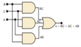
Fig 17 Implementation using gates
References:
