Combinational Logic Design
A Combinational circuit is a circuit in which we combine the different gates. For example, encoder, decoder, multiplexer, demultiplexer etc. Some of the characteristics are as follows −
Block diagram
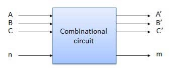
Fig: Combinational circuit (ref.2)
Key takeaway
The output of combinational circuit depends only on the levels present at input terminals at any instant of time.
It does not use any memory element
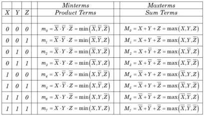
The following table represents the min terms and MAX terms for 2 variables.
x | y | Min terms | Max terms |
0 | 0 | m0=x’y’ | M0=x + y |
0 | 1 | m1=x’y | M1=x + y’ |
1 | 0 | m2=xy’ | M2=x’ + y |
1 | 1 | m3=xy | M3=x’ + y’ |
Canonical SoP and PoS forms
Therefore, we can express each output variable in two ways.
Canonical SoP form
Example
Considering the following truth table.
Inputs | Output | ||
P | q | r | f |
0 | 0 | 0 | 0 |
0 | 0 | 1 | 0 |
0 | 1 | 0 | 0 |
0 | 1 | 1 | 1 |
1 | 0 | 0 | 0 |
1 | 0 | 1 | 1 |
1 | 1 | 0 | 1 |
1 | 1 | 1 | 1 |
f = p’qr + pq’r + pqr’ + pqr.
f=m3+m5+m6+m7f=m3+m5+m6+m7
f=∑m (3,5,6,7) f=∑m (3,5,6,7)
Canonical PoS form
Standard SoP and PoS forms
Standard SoP form
Standard SoP of output variable can be obtained by two steps.
The same procedure is followed for other output variables too, if there is more than one output variable.
Standard PoS form
Standard PoS form of output variable is obtained by two steps.
The same procedure is followed for other output variables too.
Key takeaway
Numerical
Q1) Convert the Boolean function into Standard SoP form.
f = p’qr + pq’r + pqr’ + pqr
Solution:
Step 1 – By using the Boolean postulate, x + x = x and also writing the last term pqr two more times we get
⇒ f = p’qr + pq’r + pqr’ + pqr + pqr + pqr
Step 2 – By Using Distributive law for 1st and 4th terms, 2nd and 5th terms, 3rdand 6th terms.
⇒ f = qr (p’ + p) + pr (q’ + q) + pq (r’ + r)
Step 3 – Then Using Boolean postulate, x + x’ = 1 we get
⇒ f = qr (1) + pr (1) + pq (1)
Step 4 – hence using Boolean postulate, x.1 = x we get
⇒ f = qr + pr + pq
⇒ f = pq + qr + pr
This is the required Boolean function.
Q2) Convert the Boolean function into Standard PoS form.
f = (p + q + r). (p + q + r’). (p + q’ + r). (p’ + q + r)
Solution:
Step 1 – By using the Boolean postulate, x.x = x and writing the first term p+q+r two more times we get
⇒ f = (p + q + r). (p + q + r). (p + q + r). (p + q + r’). (p +q’ + r). (p’ + q + r)
Step 2 – Now by using Distributive law, x + (y.z) = (x + y). (x + z) for 1st and 4thparenthesis, 2nd and 5th parenthesis, 3rd and 6th parenthesis.
⇒ f = (p + q + rr’). (p + r + qq’). (q + r + pp’)
Step 3 − Applying Boolean postulate, x.x’=0 for simplifying of the terms present in each parenthesis.
⇒ f = (p + q + 0). (p + r + 0). (q + r + 0)
Step 4 − Using Boolean postulate, x + 0 = x we get
⇒ f = (p + q). (p + r). (q + r)
⇒ f = (p + q). (q + r). (p + r)
This is the simplified Boolean function.
Hence, both Standard SoP and Standard PoS forms are Dual to one another.
It stands for Exclusive-OR gate. Its function varies when the inputs have even number of ones.
The truth table of 2-input Ex-OR gate is:
A | B | Y = A⊕B |
0 | 0 | 0 |
0 | 1 | 1 |
1 | 0 | 1 |
1 | 1 | 0 |
Here A, B are the inputs and Y is the output of two input Ex-OR gate. The output (Y) is zero instead of one when both the inputs are one.
Therefore, the output of Ex-OR gate is ‘1’, when only one of the two inputs is ‘1’. And it is zero, when both inputs are same.
The symbol of Ex-OR gate is as follows:

Fig: XOR gate (ref. 1)
It is similar to that of OR gate with an exception for few combination(s) of inputs. Hence, the output is also known as an odd function.
Ex-OR Function Realisation using NAND gates

Fig. Realisation using NAND Gates
Exclusive-OR Gates are used mainly to build circuits that perform arithmetic operations and calculations especially Adders and Half-Adders as they can provide a “carry-bit” function or as a controlled inverter, where one input passes the binary data and the other input is supplied with a control signal.
Key takeaway
The output of Ex-OR gate is ‘1’, when only one of the two inputs is ‘1’. And it is zero, when both inputs are same.
K-Maps for 2 to 5 Variables
It is the most suitable method for minimizing Boolean functions of 2 variables to 5 variables.
2 Variable K-Map
It has 4 number of cells since the number of variables is two.
The 2 variable K-Map is:

Fig: 2 variable K-Map (ref. 1)
3 Variable K-Map
It has 8 number of cells since the number of variables is 3.
The 3 variable K-Map is:
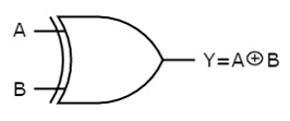
Fig: 3 variable K-Map
4 Variable K-Map
It has 16 number of cells since the number of variables is 4.
The 4 variable K-Map is:

Fig: 4 variable K-Map
Rules for simplifying K-maps:
Key takeaway
Numerical
Simplify f (X, Y, Z) =∏M (0,1,2,4) f (X, Y, Z) =∏M (0,1,2,4) using K-map.

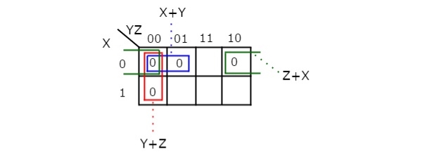
Therefore, the simplified Boolean function is
f = (X + Y). (Y + Z). (Z + X)
Simplify:
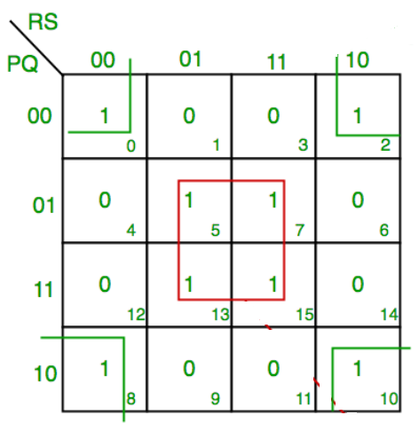
F (P, Q, R, S) =∑ (0,2,5,7,8,10,13,15)

F = P’Q’R’S’ + PQ’R’S’ + P’Q’RS’ +PQ’RS’ + QS
F = P’Q’S’ + PQ’S’ + QS
F = Q’S’ +QS
Simplify:
F (A, B, C) =π (0,3,6,7)

F = A’BC +ABC +A’B’C’ +ABC’
F = BC + C’ (A’B’ + AB)
Consider the following SOP expression F = W.X.Y + X.Y.Z + Y.Z.W
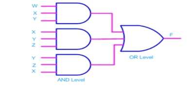
Fig: Implementation of F = W.X.Y + X.Y.Z + Y.Z.W
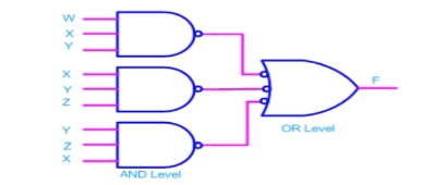
Fig: Implementation of F = W.X.Y + X.Y.Z + Y.Z.W
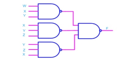
Fig: Implementation of F = W.X.Y + X.Y.Z + Y.Z.W
Realization of logic gates using NAND gates
Implementing an inverter using NAND gate
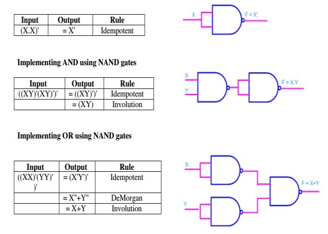

Fig: Implementation of basic gates using NAND gate
Realization of logic function using NOR gates
Consider the following POS expression F = (X+Y). (Y+Z)

Fig: Implementation of F = (X+Y). (Y+Z)
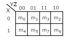
Fig: Implementation of F = (X+Y). (Y+Z)
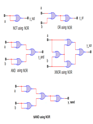
Implementing logic gates using NOR gate
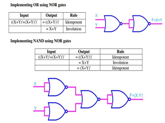
Fig: Implementation of Or and NAND gate using NOR gate
Key takeaway
2.7 Logic Components: Concept of Digital Components
A digital circuit whose outputs depend solely on the present combination of the circuit inputs’ values. Built out of simple components: switches and gates.
Electronic switches are the basis of binary digital circuits – Electrical terminology
• Voltage: Difference in electric potential between two points Analogous to water pressure
• Current: Flow of charged particles – Analogous to water flow
• Resistance: Tendency of wire to resist current flow – Analogous to water pipe diameter V I * R (Ohm’s Law)
A switch has three parts – Source input, and output
• Current wants to flow from source input to output
– Control input
• Voltage that controls whether that current can flow.
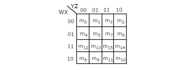
Fig: Switch
Integrated Circuits or IC’s as they are more commonly called, can be grouped together into families according to the number of transistors or “gates” that they contain.
Integrated circuits are categorised according to the number of logic gates or the complexity of the circuits within a single chip with the general classification for the number of individual gates given as:
Classification of Integrated Circuits
Small Scale Integration or (SSI) – Contain up to 10 transistors or a few gates within a single package such as AND, OR, NOT gates.
Medium Scale Integration or (MSI) – between 10 and 100 transistors or tens of gates within a single package and perform digital operations such as adders, decoders, counters, flip-flops and multiplexers.
Large Scale Integration or (LSI) – between 100 and 1,000 transistors or hundreds of gates and perform specific digital operations such as I/O chips, memory, arithmetic and logic units.
Very-Large Scale Integration or (VLSI) – between 1,000 and 10,000 transistors or thousands of gates and perform computational operations such as processors, large memory arrays and programmable logic devices.
Super-Large Scale Integration or (SLSI) – between 10,000 and 100,000 transistors within a single package and perform computational operations such as microprocessor chips, micro-controllers, basic PICs and calculators.
Ultra-Large Scale Integration or (ULSI) – more than 1 million transistors – the big boys that are used in computers CPUs, GPUs, video processors, micro-controllers, FPGAs and complex PICs.
Block diagram
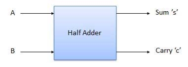
Fig: Half adder (ref. 2)
Truth Table
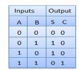
Circuit Diagram
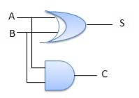
Fig: Half adder (ref. 2)
B. Full Adder
Block diagram
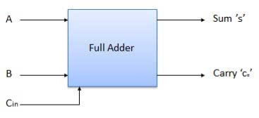
Fig: Full adder (ref. 2)
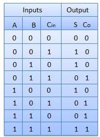
Truth Table
Circuit Diagram
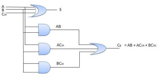
Fig: Full adder (ref. 2)
C. N-Bit Parallel Adder
4 Bit Parallel Adder
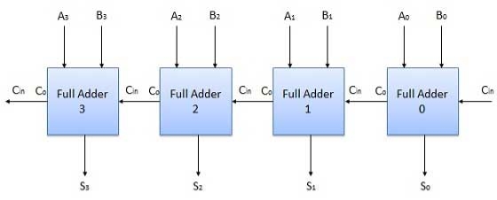
Fig: 4-bit parallel adder (ref. 2)
D. N-Bit Parallel Subtractor
4 Bit Parallel Subtractor
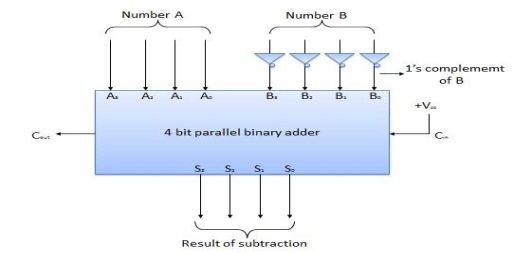
Fig: 4-bit parallel subtractor (ref. 2)
E. Half Subtractors
Truth Table
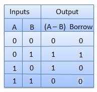
Circuit Diagram
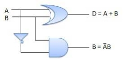
Fig: Half subtractor (ref. 2)
F. Full Subtractors
Truth Table
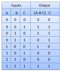
Circuit Diagram
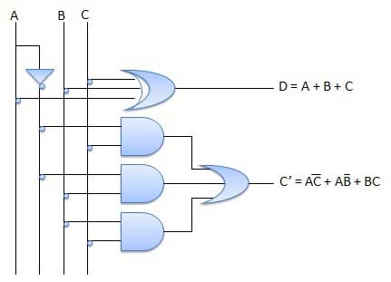
Fig: Full subtractor (ref. 2)
Carry Look-Ahead Adder

Fig: Look ahead Carry adder (ref. 2)
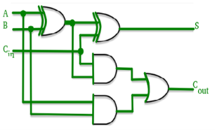
Fig: Look ahead Carry adder (ref. 2)
Advantages and Disadvantages of Carry Look-Ahead Adder:
Advantages –
Disadvantages –
Multiplier:
Multiplication of binary numbers is usually implemented in microprocessors and microcomputers by using repeated addition and shift operations. Since the binary adders are designed to add only two binary numbers at a time, instead of adding all the partial products at the end, they are added two at a time and their sum is accumulated in a register called the accumulator register. Also, when the multiplier bit is ‘0’, that very partial product is ignored, as an all ‘0’ line does not affect the final result. The basic hardware arrangement of such a binary multiplier would comprise shift registers for the multiplicand and multiplier bits, an accumulator register for storing partial products, a binary parallel adder and a clock pulse generator to time various operations.
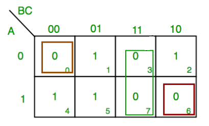
Fig: Binary Multiplier
Binary multipliers are also available in IC form. Some of the popular type numbers in the TTL family include 74261 which is a 2 × 4bit multiplier (a four-bit multiplicand designated asB0, B1, B2, B3 and B4, and a two-bit multiplier designated as M0, M1 and M2. The MSBs B4 and M2 are used to represent signs. 74284 and 74285 are 4 × 4bit multipliers. They can be used together to perform high-speed multiplication of two four-bit numbers. Figure shows the arrangement. The result of multiplication is often required to be stored in a register. The size of this register (accumulator) depends upon the number of bits in the result, which at the most can be equal to the sum of the number of bits in the multiplier and multiplicand. Some multipliers ICs have an in-built register.
Key takeaway
Half adder has two inputs and two outputs and full adder overcomes the problem faced in half adder. The full adder has three inputs including the carry bit.

Fig: N-bit comparator (ref.2)
1-Bit Magnitude Comparator –
The truth table is given below:
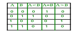
From the above truth table logical expressions for each output can be expressed as follows:
A>B: AB'
A<B: A'B
A=B: A'B' + AB
From the above expressions we can derive the following formula:
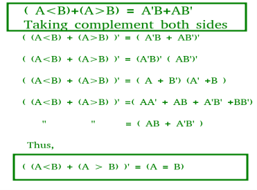
By using the above expressions, we can implement a logic circuit:

Fig: 1-bit comparator (ref.2)
2-Bit Magnitude Comparator
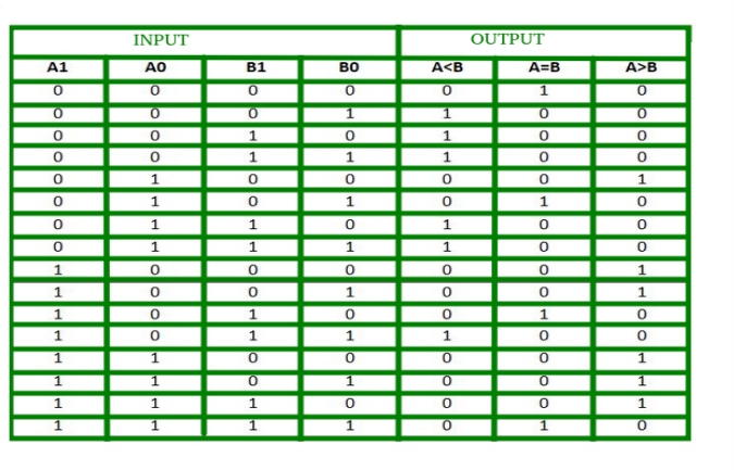
K-map for each output is as follows:
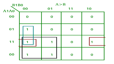
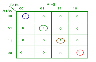
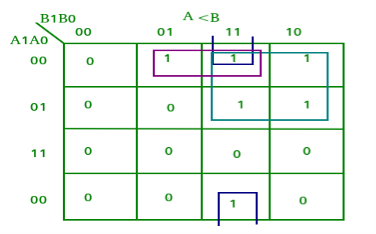
From the above K-maps output can be expressed as follows:
A>B: A1B1’ + A0B1’B0’ + A1A0B0’
A=B: A1’A0’B1’B0’ + A1’A0B1’B0 + A1A0B1B0 + A1A0’B1B0’
: A1’B1’ (A0’B0’ + A0B0) + A1B1 (A0B0 + A0’B0’)
: (A0B0 + A0’B0’) (A1B1 + A1’B1’)
: (A0 Ex-Nor B0) (A1 Ex-Nor B1)
A<B: A1’B1 + A0’B1B0 + A1’A0’B0
A logic circuit for this comparator as given below:
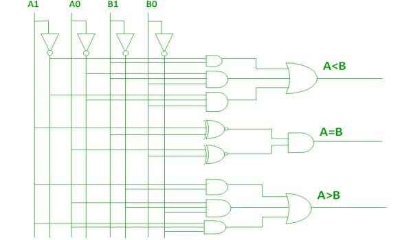
Fig: 2-bit comparator (ref.2)
4-Bit Magnitude Comparator
AA, 831331 r: (A3 Ex-Nor 33) A2132′ a (A3 Ex-Nor 133) (A2 Ex-Nor 132) A131′ a (A3 Ex-Nor 33) (A2 ENor132) (Al Ex-Nor 31) A01301 ,13: A3’03 a (A3 Ex-Nor 33) A211:12 a (A3 Ex-Nor 83) (A2 Ex-Nor 132) Ar131 a (A3 Ex-Nor 33) (A2 Ex-Nor32) (Al Ex-Nor 131) A0N30
A=B: (A3 Ex-Nor B3) (A2 Ex-Nor 82) (Al Ex-Nor BI) (AO Ex-Nor BO)
Implementation of a logic circuit for this comparator is given below:
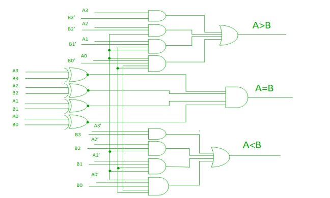
Fig: 4-bit comparator (ref.2)
Cascading Comparator –
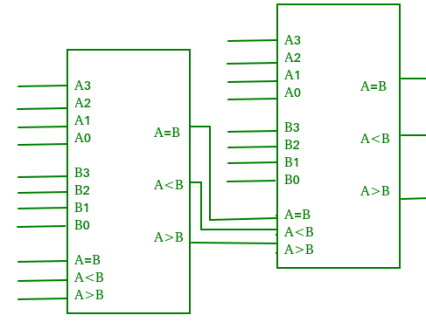
Fig: cascading comparator (ref.2)
Applications of Comparators –
Key takeaway
It is a combinational circuit which compares two binary numbers to find whether one number is equal to, less than or greater than the other number.
Truth Table –
X | Y | Z | D0 | D1 | D2 | D3 | D4 | D5 | D6 | D7 |
0 | 0 | 0 | 1 | 0 | 0 | 0 | 0 | 0 | 0 | 0 |
0 | 0 | 1 | 0 | 1 | 0 | 0 | 0 | 0 | 0 | 0 |
0 | 1 | 0 | 0 | 0 | 1 | 0 | 0 | 0 | 0 | 0 |
0 | 1 | 1 | 0 | 0 | 0 | 1 | 0 | 0 | 0 | 0 |
1 | 0 | 0 | 0 | 0 | 0 | 0 | 1 | 0 | 0 | 0 |
1 | 0 | 1 | 0 | 0 | 0 | 0 | 0 | 1 | 0 | 0 |
1 | 1 | 0 | 0 | 0 | 0 | 0 | 0 | 0 | 1 | 0 |
1 | 1 | 1 | 0 | 0 | 0 | 0 | 0 | 0 | 0 | 1 |
Implementation
D0 is high when X = 0, Y = 0 and Z = 0. Hence,
D0 = X’ Y’ Z’
Similarly,
D1 = X’ Y’ Z
D2 = X’ Y Z’
D3 = X’ Y Z
D4 = X Y’ Z’
D5 = X Y’ Z
D6 = X Y Z’
D7 = X Y Z
Hence,
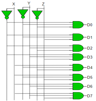
Fig: Decoder (ref.2)
Key takeaway
The decoder and demux have same internal circuit. The decoder with enable input can function as a demultiplexer. A 2x4 line decoder can act as a 1:4 demux and vice versa. Decoder contains AND gates or NAND gates.
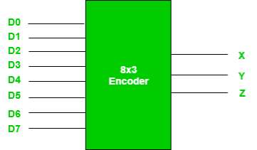
Fig: 8X3 Encoder (ref. 2)
Truth Table –
D7 | D6 | D5 | D4 | D3 | D2 | D1 | D0 | X | Y | Z |
0 | 0 | 0 | 0 | 0 | 0 | 0 | 1 | 0 | 0 | 0 |
0 | 0 | 0 | 0 | 0 | 0 | 1 | 0 | 0 | 0 | 1 |
0 | 0 | 0 | 0 | 0 | 1 | 0 | 0 | 0 | 1 | 0 |
0 | 0 | 0 | 0 | 1 | 0 | 0 | 0 | 0 | 1 | 1 |
0 | 0 | 0 | 1 | 0 | 0 | 0 | 0 | 1 | 0 | 0 |
0 | 0 | 1 | 0 | 0 | 0 | 0 | 0 | 1 | 0 | 1 |
0 | 1 | 0 | 0 | 0 | 0 | 0 | 0 | 1 | 1 | 0 |
1 | 0 | 0 | 0 | 0 | 0 | 0 | 0 | 1 | 1 | 1 |
Implementation –
X = D4 + D5 + D6 + D7
Y = D2 +D3 + D6 + D7
Z = D1 + D3 + D5 + D7
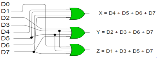
Fig: 8:3 encoder (ref.2)
Priority Encoder: –
Truth Table –
D3 | D2 | D1 | D0 | X | Y | V |
0 | 0 | 0 | 0 | x | x | 0 |
0 | 0 | 0 | 1 | 0 | 0 | 1 |
0 | 0 | 1 | x | 0 | 1 | 1 |
0 | 1 | X | x | 1 | 0 | 1 |
1 | x | X | x | 1 | 1 | 1 |
Implementation –
The condition for valid bit to be 1 is when at least one of the inputs should be high. Hence,
V = D0 + D1 + D2 + D3
For X:
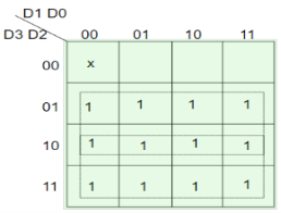
=>X=D2+D3
For Y:
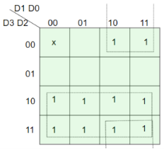
=> Y = D1 D2’ + D3
Hence, the priority 4-to-2 encoder can be realized as follows:
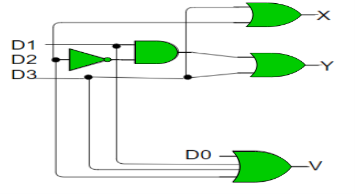
Fig: Priority encoder (ref.2)
Key takeaway
An Encoder is a combinational circuit that performs the reverse operation of Decoder. It has maximum of 2n input lines and ‘n’ output lines. It will produce a binary code equivalent to the input, which is active High.
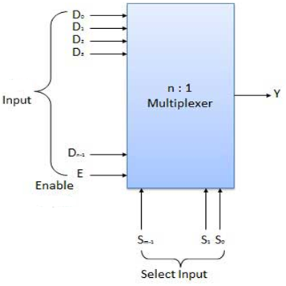
Fig: Block diagram of multiplexer (ref. 2)
Multiplexers come in multiple variations
Block Diagram of 2:1 MUX
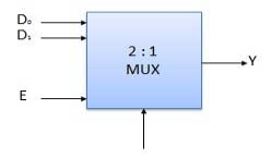
Truth Table of 2:1 MUX
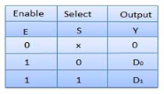
Where x is don’t care.
Demultiplexers
Various Demultiplexers are used as:
Block diagram
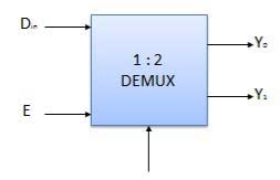
Truth Table
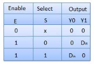
Where x is don’t care.
