Unit - 4
Binary Counters
Counter Classification
Counters are broadly classified into two categories:
1. Asynchronous Counter

Fig. 1 Asynchronous counter
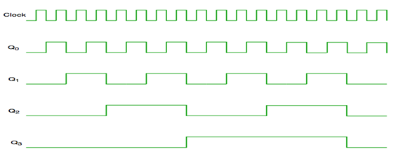
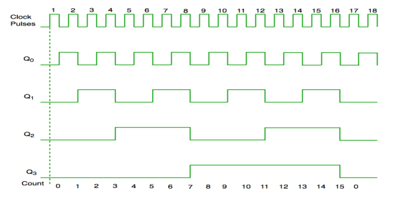
Fig. 2 Timing diagram of Asynchronous counter
2. Synchronous Counter
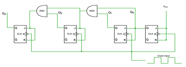
Fig. 3 synchronous counter
Fig. 4 Timing diagram of synchronous counter
Key takeaway
Counters are broadly classified into two categories:
Truth table is as follows:
Clock pulse | Q3 | Q2 | Q1 | Q0 |
0 | 0 | 0 | 0 | 0 |
1 | 0 | 0 | 0 | 1 |
2 | 0 | 0 | 1 | 0 |
3 | 0 | 0 | 1 | 1 |
4 | 0 | 1 | 0 | 0 |
5 | 0 | 1 | 0 | 1 |
6 | 0 | 1 | 1 | 0 |
7 | 0 | 1 | 1 | 1 |
8 | 1 | 0 | 0 | 0 |
9 | 1 | 0 | 0 | 1 |
10 | 0 | 0 | 0 | 0 |

Fig 5 Decade counter
In the above circuit diagram, we used NAND gate for Q3 and Q1 and sending this to clear input line as the binary representation of 10 is—
1010
And Q3 and Q1 are 1 here, if we give NAND of these two bits then counter clears at 10 and again starts from the beginning.
Up/down counters
Both Synchronous and Asynchronous counters are capable of counting “Up” or counting “Down”, but there is another more “Universal” type of counter that can count in both directions either up or down depending on the state of their input control pin and these are known as Bidirectional Counters.
Bidirectional counters, also known as Up/Down counters, are capable of counting in either direction through any given count sequence and they can be reversed at any point within their count sequence by using an additional control input as shown below.
The circuit above is of a simple 3-bit Up/Down synchronous counter using JK flip-flops configured to operate as toggle or T-type flip-flops giving a maximum count of zero (000) to seven (111) and back to zero again. Then the 3-Bit counter advances upward in sequence (0,1,2,3,4,5,6,7) or downwards in reverse sequence (7,6,5,4,3,2,1,0).
Generally, most bidirectional counter chips can be made to change their count direction either up or down at any point within their counting sequence. This is achieved by using an additional input pin which determines the direction of the count, either Up or Down and the timing diagram gives an example of the counter’s operation as this Up/Down input changes state.
Nowadays, both up and down counters are incorporated into single IC that is fully programmable to count in both an “Up” and a “Down” direction from any preset value producing a complete Bidirectional Counter chip. Common chips available are the 74HC190 4-bit BCD decade Up/Down counter, the 74F569 is a fully synchronous Up/Down binary counter and the CMOS 4029 4-bit Synchronous Up/Down counter.
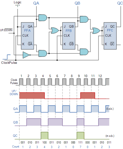
Fig 6 Up/Down Counter
Key takeaway
Both Synchronous and Asynchronous counters are capable of counting “Up” or counting “Down”, but there is another more “Universal” type of counter that can count in both directions either Up or Down depending on the state of their input control pin and these are known as Bidirectional Counters.
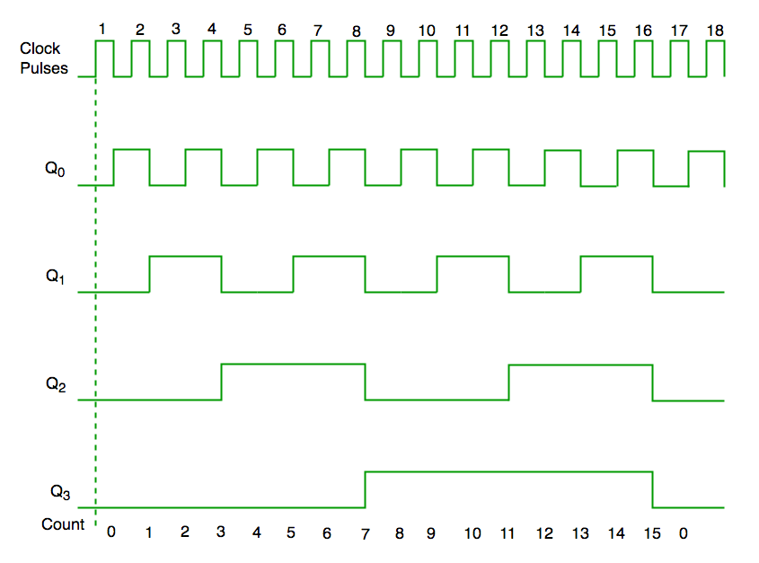

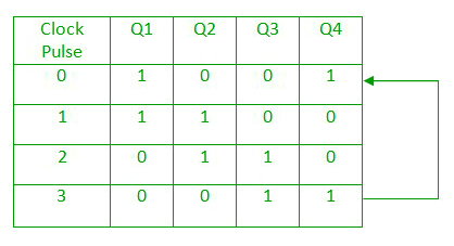
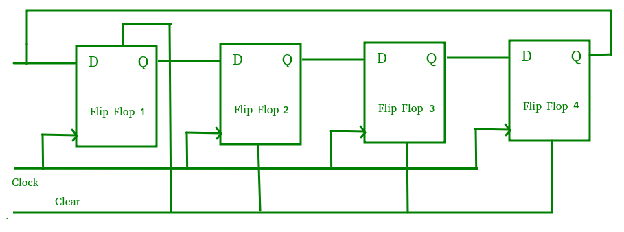
Fig. 7 Ring counter
Key takeaway
It is a shift register counter whose output of the first flip flop is connected to the second and so on and the output of the last flip flop is fed back to the input of the first flip flop, thus named as ring counter.
Truth table is as follows:
Clock pulse | Q3 | Q2 | Q1 | Q0 |
0 | 0 | 0 | 0 | 0 |
1 | 0 | 0 | 0 | 1 |
2 | 0 | 0 | 1 | 0 |
3 | 0 | 0 | 1 | 1 |
4 | 0 | 1 | 0 | 0 |
5 | 0 | 1 | 0 | 1 |
6 | 0 | 1 | 1 | 0 |
7 | 0 | 1 | 1 | 1 |
8 | 1 | 0 | 0 | 0 |
9 | 1 | 0 | 0 | 1 |
10 | 0 | 0 | 0 | 0 |
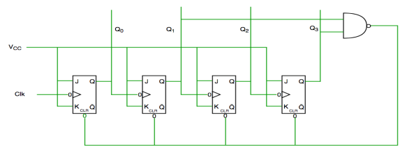
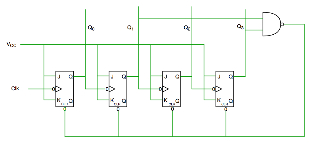
Fig. 8 Decade counter
In the above circuit diagram, we used Nand gate for Q3 and Q1 and sending this to clear input line as the binary representation of 10 is—
1010
And Q3 and Q1 are 1 here, if we give NAND of these two bits then counter clears at 10 and again starts from the beginning.
Examples
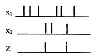
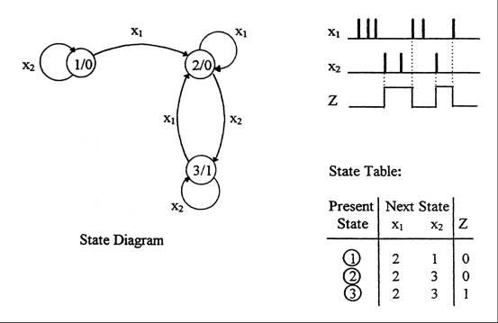
Q1) In a circuit having input pulses x1 and x2 the output z is said to be a pulse occurring with the first x2 pulse immediately following an x1 pulse.
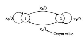
Q2) A pulsed sequential circuit has two input pulses x1, x2 and a single output Z. Z changes to logic ‘1’ with the first x2 pulse immediately following an x1 pulse. Z subsequently goes to ‘0’ when the next x1 pulse occurs
A2)
Q3) A clocked sequential circuit has two inputs x1, x2. Data on x1 and x2 are synchronized to a clock input to the circuit. Whenever x1x2 = 11 follows x1x2 = 10, the output Z is to become ‘1’. Z remains at ‘1’ until x1x2 = 00, when it returns to ‘0’.
A3)
Flip-flop is a 1-bit memory cell which can be used for storing the digital data. To increase the storage capacity in terms of number of bits, we have to use a group of flip-flops. Such a group of flip-flops is known as a Register. The n-bit register will consist of n number of flip-flop and it is capable of storing an n-bit word.
Shift registers
The registers which shift the bits towards the right are called “Shift right registers”.
Shift registers are of 4 types and they are:
Serial-In Serial-Out Shift Register (SISO) –
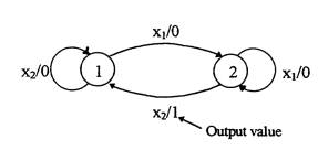
Fig 13 SISO
Serial-In Parallel-Out shift Register (SIPO) –

Fig 14 SIPO
Parallel-In Serial-Out Shift Register (PISO) –
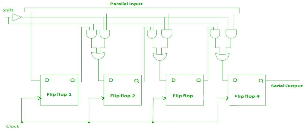
Fig 15 PISO
Parallel-In Parallel-Out Shift Register (PIPO) –
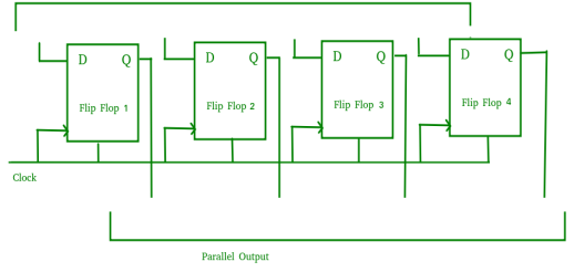
Fig 16 PIPO
Key takeaway
A logic device is an electronic component which performs a definite function which is decided at the time of manufacture and will never change. For example, a NOT Gate always inverts the logic level of the input signal and does/can-do-nothing else.
On the other hand, Programmable Logic Devices (PLDs) are the components which do not have a specific function associated with them. These can be configured to perform a certain function by the user, on a need basis and can further be changed to perform some other function at the later point of time, i.e., these are re-configurable. However, the amount of flexibility offered depends on their type. The classification of Programmable Logic Devices is as follows:
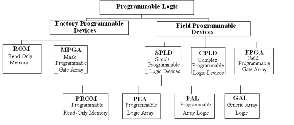
Fig 17 Programming logic devices
ECCs are of two types −
Hamming Code
Encoding a message by Hamming Code
It requires the following steps −
Step 1 − Calculating the number of redundant bits.
Step 2- Positioning them.
Step 3 − Calculating the values of each of the redundant bits
Even Parity − where the total number of bits in the message is even.
Odd Parity − where the total number of bits in the message is odd.
Decoding a message in Hamming Code
Once the receiver gets an incoming message, recalculations are done to detect errors and correct them. The steps for recalculation are −
Step 1 − Calculation of the number of redundant bits
Using the same method as in encoding, the number of redundant bits are ascertained.
2r ≥ m + r + 1
where m is and r have their usual meaning.
Step 2 − Positioning the redundant bits
The r redundant bits placed at bit positions of powers of 2.
Step 3 − Parity checking
They are calculated on the basis of the data bits and the redundant bits using the same rule as during generation. Thus,
c1 = parity (1, 3, 5, 7, 9, 11 and so on)
c2 = parity (2, 3, 6, 7, 10, 11 and so on)
c3 = parity (4 to7, 12-15, 20 to 23 and so on)
Step 4 − Error detection and correction
The decimal equivalent of the parity bits is calculated. If it is a 0, then there is no error. Else, the decimal value gives the bit position which has error.
For example, if c1c2c3c4 = 1000, it implies that the data bit at position 8, decimal equivalent of 1000, has error.
The bit is flipped to get the correct message.
Key takeaway
Hamming Codes
To meet the growing needs for semiconductor memory, there are many types and technologies that are used. As the demand grows new memory technologies are being introduced and the existing types and technologies are being further developed.
There are two main types or categories that can be used for semiconductor technology. These memory types or categories differentiate the memory to the way in which it operates:
RAM - Random Access Memory: As the names suggest, the RAM or random access memory is a form of semiconductor memory technology that is used for reading and writing data in any order - in other words as it is required by the processor. It is used for such applications as the computer or processor memory where variables and other stored and are required on a random basis. Data is stored and read many times to and from this type of memory.
Random access memory is used in huge quantities in computer applications as current day computing and processing technology requires large amounts of memory to enable them to handle the memory hungry applications used today. Many types of RAM including SDRAM with its DDR3, DDR4, and soon DDR5 variants are used in huge quantities.
ROM - Read Only Memory: A ROM is a form of semiconductor memory technology used where the data is written once and then not changed. In view of this it is used where data needs to be stored permanently, even when the power is removed - many memory technologies lose the data once the power is removed.
As a result, this type of semiconductor memory technology is widely used for storing programs and data that must survive when a computer or processor is powered down. For example, the BIOS of a computer will be stored in ROM. As the name implies, data cannot be easily written to ROM. Depending on the technology used in the ROM, writing the data into the ROM initially may require special hardware. Although it is often possible to change the data, this gain requires special hardware to erase the data ready for new data to be written in.
Each of the semiconductor memory technologies outlined below falls into one of these two types of categories. Each technology offers its own advantages and is used in a particular way, or for a particular application.
1) EPROM
This is an Erasable Programmable Read Only Memory. These semiconductor devices can be programmed and then erased at a later time. This is normally achieved by exposing the semiconductor device itself to ultraviolet light. To enable this to happen there is a circular window in the package of the EPROM to enable the light to reach the silicon of the device. When the PROM is in use, this window is normally covered by a label, especially when the data may need to be preserved.
The PROM stores its data as a charge on a capacitor. There is a charge storage capacitor for each cell and this can be read repeatedly as required. However, it is found that after many years the charge may leak away and the data may be lost. Nevertheless, this type of semiconductor memory used to be widely used in applications where a form of ROM was required, but where the data needed to be changed periodically, as in a development environment, or where quantities were low.
2) EEPROM
This is an Electrically Erasable Programmable Read Only Memory. Data can be written to these semiconductor devices and it can be erased using an electrical voltage. This is typically applied to an erase pin on the chip. Like other types of PROM, EEPROM retains the contents of the memory even when the power is turned off. Also, like other types of ROM, EEPROM is not as fast as RAM.
3) DRAM
Dynamic RAM is a form of random access memory. DRAM uses a capacitor to store each bit of data, and the level of charge on each capacitor determines whether that bit is a logical 1 or 0.
However, these capacitors do not hold their charge indefinitely, and therefore the data needs to be refreshed periodically. As a result of this dynamic refreshing, it gains its name of being a dynamic RAM. DRAM is the form of semiconductor memory that is often used in equipment including personal computers and workstations where it forms the main RAM for the computer. The semiconductor devices are normally available as integrated circuits for use in PCB assembly in the form of surface mount devices or less frequently now as leaded components.
4) SRAM
This form of semiconductor memory gains its name from the fact that, unlike DRAM, the data does not need to be refreshed dynamically. These semiconductor devices are able to support faster read and write times than DRAM (typically 10 ns against 60 ns for DRAM), and in addition its cycle time is much shorter because it does not need to pause between accesses. However, they consume more power, they are less dense and more expensive than DRAM. As a result of this SRAM is normally used for caches, while DRAM is used as the main semiconductor memory technology.
5) NVRAM
NVRAM is random-access memory that retains its information when power is turned off (non-volatile). This is in contrast to dynamic, random-access memory (DRAM) and static random-access memory (SRAM), which both maintain data only for as long as power is applied. The best-known form of NVRAM memory today is flash memory.
Key takeaway
RAM - Random Access Memory: As the names suggest, the RAM or random access memory is a form of semiconductor memory technology that is used for reading and writing data in any order - in other words as it is required by the processor.
ROM - Read Only Memory: A ROM is a form of semiconductor memory technology used where the data is written once and then not changed. In view of this it is used where data needs to be stored permanently, even when the power is removed - many memory technologies lose the data once the power is removed.
The combinational circuit do not use all the minterms every time. Occasionally they have don’t care conditions. Don’t care condition when implemented with a PROM becomes an address input that will never occur. The result is that not all the bit patterns available in the PROM are used, which may be considered a waste of available equipment.
For cases where the number of don’t care conditions is excessive, it is more economical to use Programmable Logic Array (PLA). The concept is similar to PROM, however it does not generate all the minterms as in the case of PROM. It has both sections of the AND and OR Arrays as programmable, i.e., there is a Programmable AND Array and Programmable OR Array as well. (Both AND and OR gates have fuses at the inputs).
The following figure shows the block diagram of PLA:
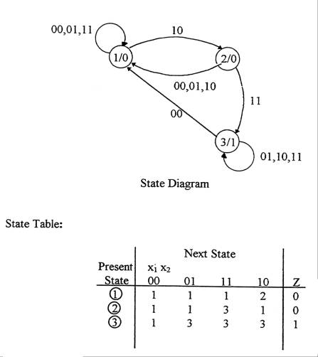
Fig 18 Block Diagram of PLA
It consists of n-inputs, m outputs, k-product terms and m sum terms. The product terms constitute a group of k AND gates and the sum terms constitute a group of m OR gates. Fuses are inserted between all n inputs and their complement values to each of the AND gates. Fuses are also provided between the outputs of the AND gates and the inputs of the OR Gates. The third set of fuses in the output inverters allows the output function to be generated either in the AND-OR form or in the AOI form.
The following figure shows the internal construction of PLA having 3-inputs, 3 product terms and two outputs. The size of the PLA is specified by the number of inputs, the number of product terms and the number of outputs.
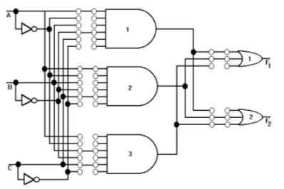
Fig 19 Internal Construction of PLA
Key takeaway
The concept is similar to PROM; however, it does not generate all the min-terms as in the case of PROM. It has both sections of the AND and OR Arrays as programmable, i.e., there is a Programmable AND Array and Programmable OR Array as well. (Both AND and OR gates have fuses at the inputs).
Programmable array logic (PAL) is a programmable logic device with a fixed OR array and a programmable AND array. Because only AND gates are programmable, PAL is easier to program, but is not as flexible as the PLA. Figure below shows the array logic of typical PAL.
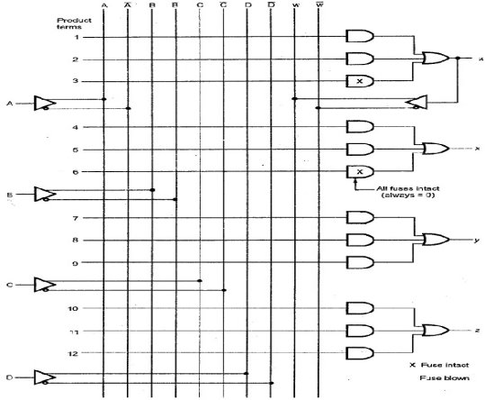
Fig 20 PAL
It has 4 inputs and 4 outputs. Each input has buffer and inverter gate. Please note that two gates are shown with one composite graphic symbol with normal and complement outputs. Each section in the figure has three programmable AND gates and one fixed OR gate. The output of section 1 is connected to a buffer-inverter gate and then feedback into the inputs of the AND gates, through fuses. This allows the logic designer to feed an output function back as an input variable to create a new function.
Key takeaway
Programmable array logic (PAL) is a programmable logic device with a fixed OR array and a programmable AND array. Because only AND gates are programmable, PAL is easier to program, but is not as flexible as the PLA. Figure below shows the array logic of typical PAL.
Digital systems are designed with flip-flops and gates. Since the combinational PLD consists of only gates, it is necessary to include external flip-flops when they are used in the design. Sequential programmable devices include both gates and flip-flops. Therefore, we will describe three major types without going into their detailed construction:
1. Sequential (or simple) programmable logic device (SPLD)
2. Complex programmable logic device (CPLD)
3. Field‐programmable gate array (FPGA)
1. Sequential (or simple) programmable logic device (SPLD) The sequential PLD is sometimes referred to as a simple PLD to differentiate it from the complex PLD. The SPLD includes flip‐flops, in addition to the AND–OR array, within the integrated circuit chip. The result is a sequential circuit as shown in Figure. A PAL or PLA is modified by including a number of flip‐flops connected to form a register. The circuit outputs can be taken from the OR gates or from the outputs of the flip‐flops.

Fig 21 Sequential Programmable Logic Device
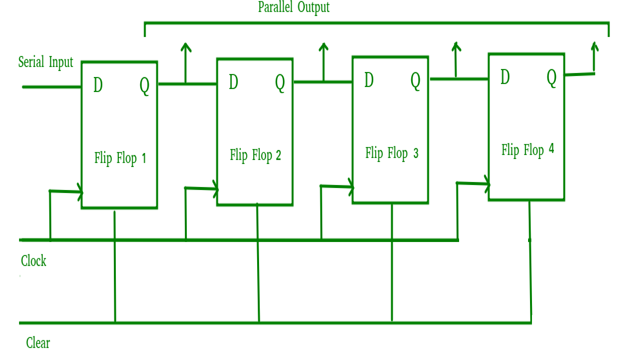
Fig 22 Basic Micro cell
Additional programmable connections are available to include the flip‐flop outputs in the product terms formed with the AND array. The flip‐flops may be of the D or the JK type. The configuration mostly used in an SPLD is the combinational PAL together with D flip‐flops. A PAL that includes flip‐flops is referred to as a registered PAL, to signify that the device contains flip‐flops in addition to the AND–OR array. Each section of an SPLD is called a macrocell, which is a circuit that contains a sum‐of‐products combinational logic function and an optional flip‐flop.
Figure shows the logic of a basic macrocell. The AND–OR array is the same as in the combinational PAL. The output is driven by an edge‐triggered D flip‐flop connected to a common clock input and changes state on a clock edge. The output of the flip‐flop is connected to a three‐state buffer (or inverter) controlled by an output‐enable signal marked in the diagram as OE. The output of the flip‐flop is fed back into one of the inputs of the programmable AND gates to provide the present‐state condition for the sequential circuit. A typical SPLD has from 8 to 10 macrocells within one IC package. All the flip‐flops are connected to the common CLK input, and all three‐state buffers are controlled by the OE input.
FPGAs are based on gate array technology unlike the PROM technology of early PLDs. These devices comprise of configurable logic blocks (CLBs) along with an interconnection matrix running in-between. FPGAs work based upon the look-up tables (LUTs) and the flip-flops which form a part of CLB. The user has to program the CLBs to perform a certain logical function and then use the interconnection matrix to connect one or more logic blocks together. Further, they comprise of input-output (I/O) ports facilitating the design both from the point of programming as well as debugging.
These devices are capable of implementing state-machine based sequential designs along with the designs based on combinational logic. FPGAs are used to realize more complex designs when compared to CPLDs due to their high density. Moreover, FPGAs offer the customer the flexibility to design/re-design the logic even after being deployed in the work field which gives them the name field-programmable.
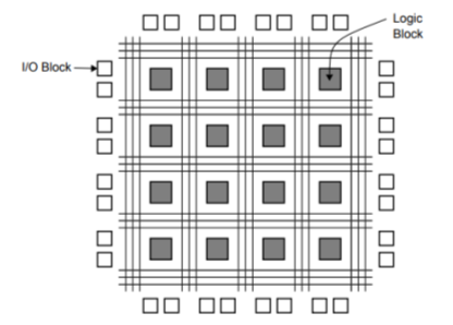
Fig 23: Architecture of FPGA
CPLD
CPLDs are denser than PALs and comprise of a large number of programmable logical elements. The interconnection between these macro cells is to be established by the user through the interconnecting network. Here sum-of-product establishing logical elements are combined together to form structures in order to reduce the number of input-output (IO) pins. This facilitates the implementation of more complex logic design with slightly worse propagation time when compared to that of PALs. These offer predictable timing characteristics making them most suitable for critical control applications with high performance. CPLDs are preferred to implement combinational logic-based designs.
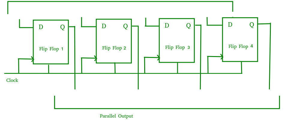
Fig 24: Architecture of CPLDs
The building block of the CPLD is the macro cell, which contains logic implementing disjunctive normal form expressions and more specialized logic operations.
The programmable interconnect in the centre allows connection to the logic block macro cells and the I/O cell arrays.
Key takeaway
Three major types without going into their detailed construction:
1. Sequential (or simple) programmable logic device (SPLD)
2. Complex programmable logic device (CPLD)
3. Field‐programmable gate array (FPGA)
References:
