Unit - 5
IC Logic Families
- Power Dissipation: Power dissipation of a circuit defines its battery life: the greater the power dissipation, the shorter the battery life. It is directly proportional to the heat generated by the chip or system hence excessive heat dissipation may increase operating temperature and cause gate circuitry to drift out of its normal operating range.
- Power Supply Requirements: There is normally one power supply to the chip denoted as Vcc. The main requirement for ICs is low power consumption.
DTL Logic Family
The diode-transistor logic, also termed as DTL, replaced RTL family because of greater fan-out capability and more noise margin. As its name suggests, DTL circuits mainly consists of diodes and transistors that comprises DTL devices.
The basic DTL device is a NAND gate, shown aside. Three inputs to the gate are applied through three diodes viz. D1, D2 and D3. The diode will conduct only when corresponding input is LOW.
If any of the diode is conducting i.e., when at least one input is LOW, the voltage at cathode of diode DA is such that it keeps transistor T in cut-off and subsequently, output of transistor is HIGH.
If all inputs are HIGH, all diodes are non-conducting, transistor T is in saturation, and its output is LOW.
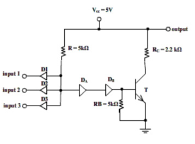
Fig 1 DTL Logic
Due to number of diodes used in this circuit, the speed of the circuit is significantly low. Hence this family of logic gates is modified to transistor-transistor logic i.e., TTL family.
RTL Logic
As its name suggests, RTL circuits mainly consists of resistors and transistors that comprises RTL devices.
The basic RTL device is a NOR gate, shown in figure.
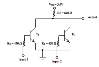
Fig 2 RTL Logic
Inputs to the NOR gate shown above are ‘input1’ & ‘input2’. The inputs applied at these terminals represent either logic level HIGH (1) or LOW (0). The logic level LOW is the voltage that drives corresponding transistor in cut-off region, while logic level HIGH drives it into saturation region.
If both the inputs are LOW, then both the transistors are in cut-off i.e., they are turned-off. Thus, voltage Vcc appears at output i.e., HIGH. If either transistor or both of them are applied HIGH input, the voltage Vcc drops across Rc and output is LOW.
RTL family is characterized by poor noise margin, poor fan-out capability, low speed and high-power dissipation. Due to these undesirable characteristics, this family is now obsolete.
I2L Logic
Its main advantage is its high packing density of gates that can be achieved in a given area of semiconductor chip. This allows more circuits to be placed in the chip. The circuit is shown below.
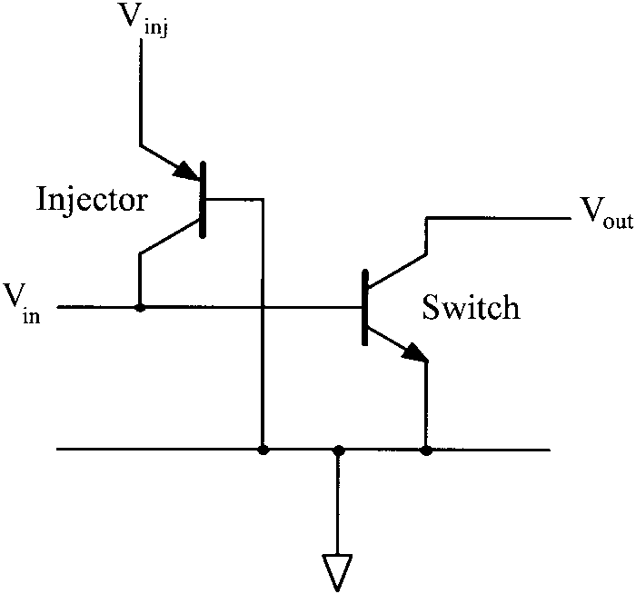
Fig 3 I2L
The I2L basic gate is similar to RTL gate as
TTL: Standard TTL characteristics
They are built only with the help of transistors.
It has been improved to meet performance requirements.
TTL family comprises of:
Operation of TTL NAND Gate (Two input)
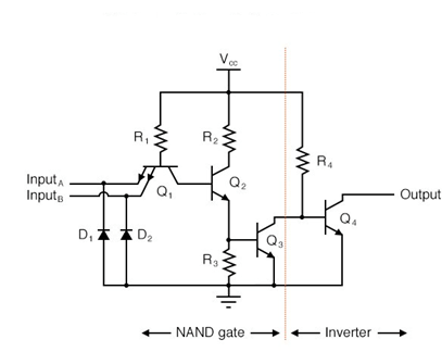
The circuit diagram of a 2 input TTL NAND gate is as follows:
a) A and B both low: both B-E junctions of Q1 are forward biased. Hence D1 and D2 will conduct to force the voltage at point C to 0.7V. This voltage is insufficient to forward bias B-E junction of Q2. Hence Q2 remains OFF. Therefore, its collector voltage rises to VCCVCC. As Q3 is operating in emitter follower mode, output Y will be pulled up to high voltage Y= 1
b) Either A or B low: If any one input is connected to ground with other left open or connected to VCCVCC the corresponding diode (D1 or D2) will conduct. This will pull down voltage at C o 0.7V. This voltage is insufficient to turn on Q2 so it remains OFF. So, collector voltage of Q2 will be equal to VCC. This voltage acts as base voltage for Q3. As Q3 acts as an emitter follower, output Y will be pulled to VCCVCC. Y= 1
c) A and B both high: If both A and B are connected to then both diodes D1 and D2 will be reverse biased and do not conduct. Therefore, D3 is forward biased and base current is supplied to transistor Q2 via R1 and D3. As Q2 conducts, the voltage at X will drop down and Q3 will be OFF, whereas voltage at Z will increase to turn ON Q4. As Q4 goes into saturation, the output voltage Y will be pulled down to low. Y = 0
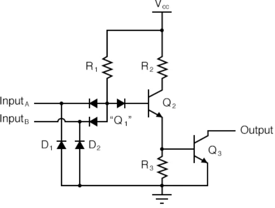
Fig 4 TTL NAND Gate Logic
TTL with active pull up
It is possible in TTL gates the charging of output capacitance without corresponding increase in power dissipation with the help of an output circuit arrangement referred to as an active pull-up or totem-pole output. In this case,
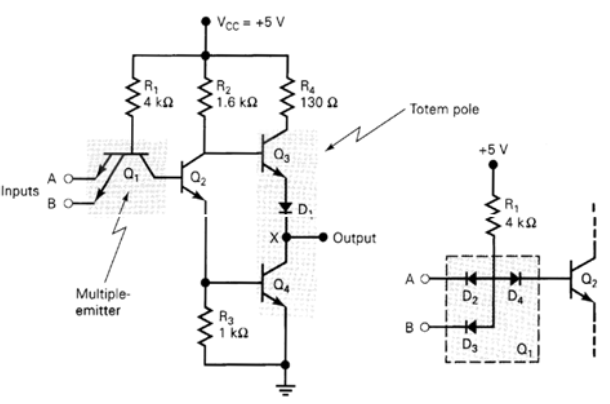
Fig 5 TTL Active Pull Up
TTL with open collector output
The main feature is that its output is 0 when low and floating when high. Usually, an external Vcc may be applied.
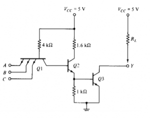
Fig 6 TTL with open collectorTransistor
Q1 behaves as a cluster of diodes placed back-to-back. With any of the input at logic low, the corresponding emitter-base junction is forward biased and the voltage drop across the base of Q1 is around 0.9V, not enough for the transistors Q2 and Q3 to conduct. Thus, the output is either floating or Vcc, i.e., High level.
Similarly, when all inputs are high, all base-emitter junctions of Q1 are reverse biased and transistor Q2 and Q3 get enough base current and are in saturation mode. The output is at logic low. (For a transistor to go to saturation, collector current should be greater than β times the base current).
Totem Pole Output:
Totem Pole means the addition of an active pull up the circuit in the output of the Gate which results in a reduction of propagation delay.

Fig 7 Totem Pole Output
Logic operation is the same as the open collector output. The use of transistors Q4 and diode is to provide quick charging and discharging of parasitic capacitance across Q3. The resistor is used to keep the output current to a safe value.
Three state Gate:
It provides 3 state output.
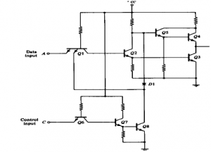
Fig 8 Three state Gate TTL
Operation of TTL NAND gate
In the single-input (inverter) circuit, grounding the input resulted in an output that assumed the “high” (1) state. In the case of the open-collector output configuration, this “high” state was simply “floating.”
Allowing the input to float (or be connected to Vcc) resulted in the output becoming grounded, which is the “low” or 0 state. Thus, a 1 in resulted in a 0 out, and vice versa.
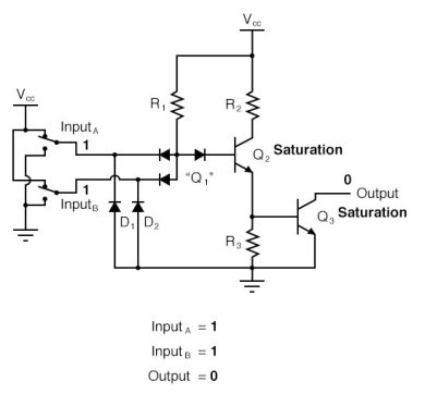
Fig 9 Operation of NAND Gate
AND
To create an AND function using TTL circuitry, we need to increase the complexity of this circuit by adding an inverter stage to the output, just like we had to add an additional transistor stage to the TTL inverter circuit to turn it into a buffer:
Of course, both NAND and AND gate circuits may be designed with totem-pole output stages rather than open-collector. I am opting to show the open-collector versions for the sake of simplicity.
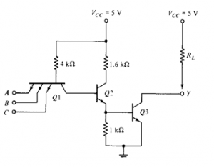
Fig 10 Operation of AND Gate
CMOS Inverter
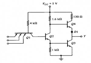
Fig 11: CMOS inverter
A | Y = A’ |
0 | 1 |
1 | 0 |

Fig 12: NOT gate (ref. 1)
CMOS characteristics
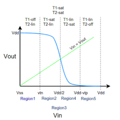
The VTC is divided into five regions (1-5) for easy of understanding. The above shown curve is possible when both T1 and T2 are matched for optimum operation. Optimum operation is achieved when Vin = Vdd/2 we get Vout = Vdd/2. This can be achieved by adjusting width and length of both T1 and T2 as other parameters like mobility, oxide capacitance varies between different technologies.

Region-1
In this, the input is in the range of (0, Vtn).
Region-2
Here, the input is in the range of (Vtn, Vdd/2).
Region-3
Here the input voltage is Vdd/2. At this point the output voltage is Vdd/2. Here both the NMOS and PMOS are in saturation and the output drops drastically from Vdd to Vdd/2. At this point a large amount of current flows from the supply.
Region-4
In this region the input voltage is in the range of (Vdd/2, Vdd-Vtp). Here the PMOS remains in saturation as Vout < Vin - Vtp and Vgsp < Vtp. But the NMOS moves from saturation to linear region since the drain to source voltage now is less than Vgsn-Vtn.
Region-5
In this region the input voltage is in the range of (Vdd-Vtp, Vdd). Here the PMOS moves from saturation to cutoff as the Vgsp is so high that Vgsp > Vtp. The NMOS still remains in linear as the drain to source voltage now is less than Vgsn-Vtn.
CMOS configurations- Wired Logic, Open-drain outputs
Open Drain is a type of programmable output port configuration with push pull, input only, and quasi-bidirectional configurations. Open-collector/open-drain is a circuit technique which allows multiple devices to communicate bidirectionally on a single wire. This is basically a mode which provides just a pull-down operation.
An open collector/open drain is a common type of output found on many integrated circuits (IC). Instead of outputting a signal of a specific voltage or current, the output signal is applied to the base of an internal NPN transistor whose collector is externalized (open) on a pin of the IC. The emitter of the transistor is connected internally to the ground pin. If the output device is a MOSFET the output is called open drain and it functions in a similar way.
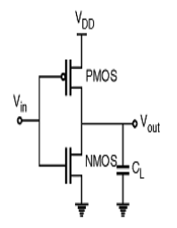
Fig 13 Open Drain CMOS
Operation of CMOS NAND gate
The CMOS NAND Gate is shown below. It has two transistors Q1 and Q3 connected in series and having the same input A. The transistor Q1 is turned ON when the input is high and the transistor Q3 is turned OFF during that period and vice versa.
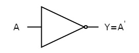
Fig 14: CMOS NAND Gate
The transistors Q2 and Q4 are connected in series having same input B. The transistors Q1 and Q2 have their source and drain connected in parallel. So, when any of the transistor amongst the two saturates the output goes HIGH. The transistors Q3 and Q4 have their source and drain connected in series. When both these transistors saturate the output goes LOW.
Key takeaway
A/D converters
A converter that is used to change the analog signal to digital is known as an analog to digital converter or ADC converter. This converter is one kind of integrated circuit or IC that converts the signal directly from continuous form to discrete form. ADC is available in different types and some of the types of analog to digital converters include:
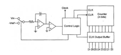
Dual Slope A/D Converter
In this type of ADC converter, comparison voltage is generated by using an integrator circuit which is formed by a resistor, capacitor, and Op-Amp combination. By the set value of Vref, this integrator generates a sawtooth waveform on its output from zero to the value Vref. When the integrator waveform is started correspondingly counter starts counting from 0 to 2^n-1 where n is the number of bits of ADC.
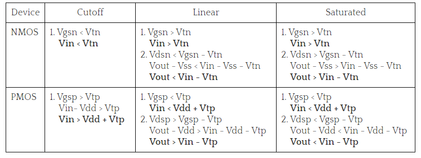
Fig 15 Dual Slope Converter
When the input voltage Vin equal to the voltage of the waveform, then the control circuit captures the counter value which is the digital value of the corresponding analog input value. This Dual slope ADC is a relatively medium cost and slow speed device
Flash A/D Converter
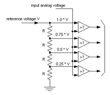
This ADC converter IC is also called parallel ADC, which is the most widely used efficient ADC in terms of its speed. This flash analog to digital converter circuit consists of a series of comparators where each one compares the input signal with a unique reference voltage. At each comparator, the output will be a high state when the analog input voltage exceeds the reference voltage. This output is further given to the priority encoder for generating binary code based on higher-order input activity by ignoring other active inputs. This flash type is a high-cost and high-speed device.
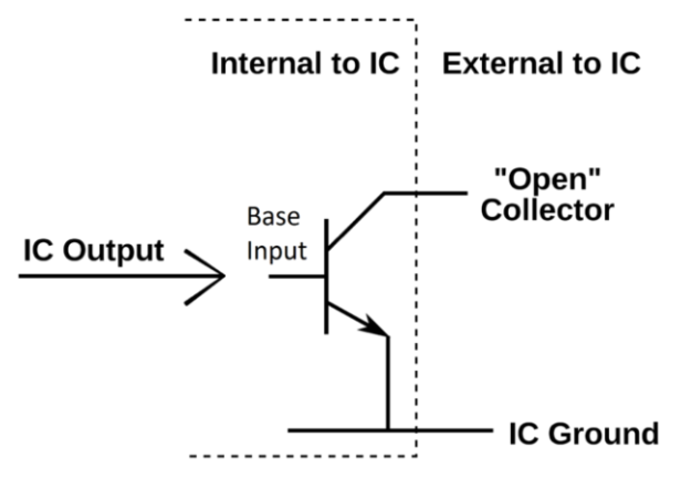
Fig 16 Flash A/D Converter
Successive Approximation A/D Converter
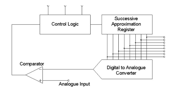
The SAR ADC a most modern ADC IC and much faster than dual slope and flash ADCs since it uses a digital logic that converges the analog input voltage to the closest value. This circuit consists of a comparator, output latches, successive approximation register (SAR), and D/A converter.
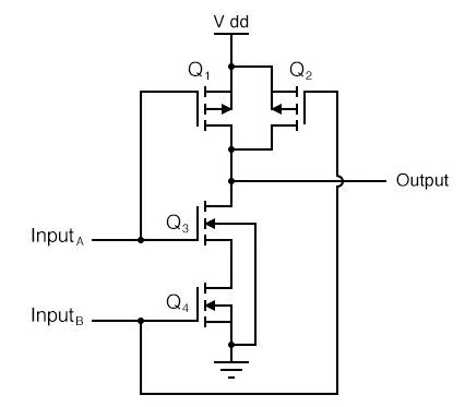
Fig 17 Successive Approximation A/D Converter
At the start, SAR is reset and as the LOW to HIGH transition is introduced, the MSB of the SAR is set. Then this output is given to the D/A converter that produces an analog equivalent of the MSB, further it is compared with the analog input Vin. If comparator output is LOW, then MSB will be cleared by the SAR, otherwise, the MSB will be set to the next position. This process continues till all the bits are tried and after Q0, the SAR makes the parallel output lines to contain valid data.
D/A converters
A Digital to Analog Converter (DAC) converts a digital input signal into an analog output signal. The digital signal is represented with a binary code, which is a combination of bits 0 and 1. A Digital to Analog Converter (DAC) consists of a number of binary inputs and a single output. In general, the number of binary inputs of a DAC will be a power of two.
Types of DACs
There are two types of DACs
This section discusses about these two types of DACs in detail −
Weighted Resistor DAC
A weighted resistor DAC produces an analog output, which is almost equal to the digital (binary) input by using binary weighted resistors in the inverting adder circuit. In short, a binary weighted resistor DAC is called as weighted resistor DAC.
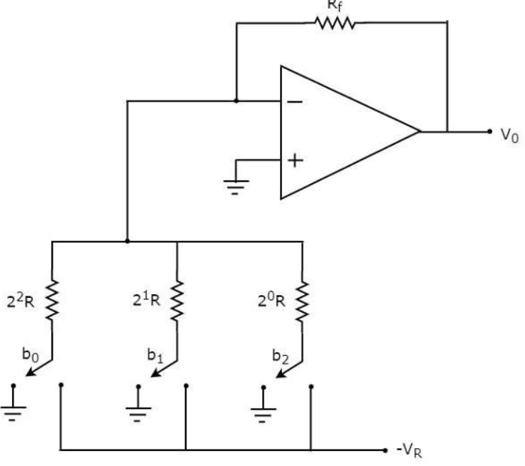
The circuit diagram of a 3-bit binary weighted resistor DAC is shown in the following figure −
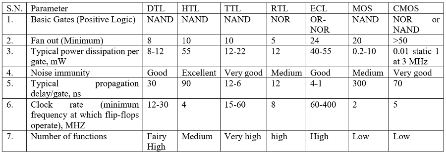
Fig 18 Weighted Resistor DAC
Here, the bits b2 and b0 denote the Most Significant Bit (MSB) and Least Significant Bit (LSB) respectively. The digital switches shown in the above figure will be connected to ground, when the corresponding input bits are equal to ‘0’. Similarly, the digital switches shown in the above figure will be connected to the negative reference voltage, −VR when the corresponding input bits are equal to ‘1’.
In the above circuit, the non-inverting input terminal of an op-amp is connected to ground. That means zero volts is applied at the non-inverting input terminal of op-amp.
According to the virtual short concept, the voltage at the inverting input terminal of opamp is same as that of the voltage present at its non-inverting input terminal. So, the voltage at the inverting input terminal’s node will be zero volts.
The nodal equation at the inverting input terminal’s node is:

The above equation represents the output voltage equation of a 3-bit binary weighted resistor DAC. Since the number of bits are three in the binary (digital) input, we will get seven possible values of output voltage by varying the binary input from 000 to 111 for a fixed reference voltage, VRVR.
We can write the generalized output voltage equation of an N-bit binary weighted resistor DAC as shown below based on the output voltage equation of a 3-bit binary weighted resistor DAC.

R-2R Ladder DAC
he R-2R Ladder DAC overcomes the disadvantages of a binary weighted resistor DAC. As the name suggests, R-2R Ladder DAC produces an analog output, which is almost equal to the digital (binary) input by using a R-2R ladder network in the inverting adder circuit.
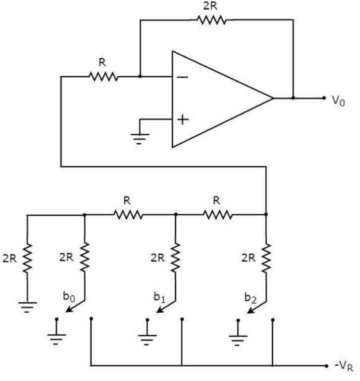
The circuit diagram of a 3-bit R-2R Ladder DAC is shown in the following figure

Fig 19 R-2R Ladder DAC
Here, the bits b2 and b0 denote the Most Significant Bit (MSB) and Least Significant Bit (LSB) respectively.
The digital switches shown in the above figure will be connected to ground, when the corresponding input bits are equal to ‘0’. Similarly, the digital switches shown in above figure will be connected to the negative reference voltage, −VR when the corresponding input bits are equal to ‘1’.
It is difficult to get the generalized output voltage equation of a R-2R Ladder DAC. But we can find the analog output voltage values of R-2R Ladder DAC for individual binary input combinations easily.
Key takeaway
The advantages of a R-2R Ladder DAC are as follows
This is reason R-2R are preferred over binary weighted resistor.

VHDL Capabilities
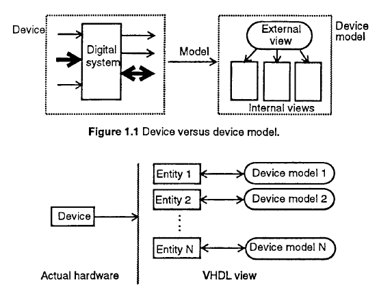
 VHDL view of a device

Fig.20: VHDL view (ref 4)
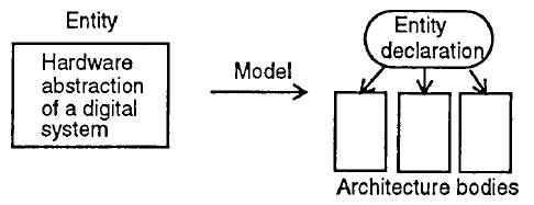
ENTITY BLOCK
entity entity_name is
port (signal_name, signal_name: mode type;
signal_name, signal_name: mode type); end entity_name;

Fig.21: Entity and its model (ref 4)
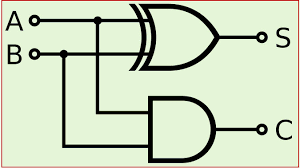
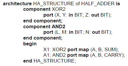
Here is an example of an entity declaration for a half adder
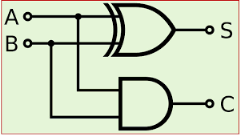
Fig.22: Half adder (ref 4)
entity hf is
port (A, B: in std_logic;
Sum, Carry: out std_logic);
end hf;
ARCHITECTURE BLOCK

architecture arch_name of entity_name is declarations;
begin
statements defining operation;
end arch_name;
library ieee;
use ieee.std_logic_1164.all;
-- entity block
entity hf is
port (A, B: in std_logic;
Sum, Carry: out std_logic);
end hf;
-- architecture block architecture hf1 of hf is
begin
-- assignment statements
{
Sum<= a xor b;
Carry <= a and b;
}
end hf1;
Modeling Styles
There are 3 types of modeling styles:
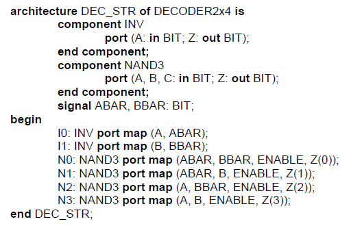
Structural Modeling

A structural representation of 2X4 decoder is given by:
Data Flow Modeling

Behavioral Modeling
VHDL Sequential Statements
Sequential Statements
Wait statement
SYNTAX:
[ label:] wait [ sensitivity clause] [ condition clause];
For Example:
wait for 10 ns; -- timeout clause, specific time delay.
entity FF is
port (D, CLK: in bit;
Q : out bit);
end FF;
architecture BEH_1 of FF is begin
process
begin
wait on CLK;
if (CLK = '1') then
Q<=D;
end if;
end process;
 end BEH_1;
Assertion statement
SYNTAX:
[ label:] assert boolean_condition [ report string] [ severity name];
For Example:
assert a= (b or c);
Report statement
It is used for output messages.
SYNTAX:
[ label:] report string [ severity name];
report "finished pass1";
Signal assignment statement
SYNTAX:
[ label:] target <= [ delay_mechanism] waveform;
For Example:
 delay_mechanism transport reject time_expression inertialwaveform
waveform_element [, waveform_element]
unaffected
Variable assignment statement
SYNTAX:
[ label:] target: = expression;
For Example:
architecture RTL of XYZ is
signal A, B, C: integer range 0 to 7;
signal Y, Z: integer range 0 to 15; begin

process (A, B, C)
variable M, N: integer range 0 to 7;
begin
M: =A;
N: =B;
Z<=M+N;
M: =C;
Y<=M+N;
end process;
end RTL;
Procedure call statement
SYNTAX:
[ label:] procedure-name [ (actual parameters)];
For Example:
do_it; -- no actual parameters
compute (stuff, A=>a, B=>c+d); -- positional association first,
--formal parameters to actual parameters
If statement
SYNTAX:
if CONDITION then
-- sequential statements end if;

if CONDITION then
-- sequential statements
else
-- sequential statements end if;
For Example:
entity IF_STATEMENT is
port (A, B, C, X: in bit_vector (3 downto 0);
Z: out bit_vector (3 downto 0); end IF_STATEMENT;
architecture EXAMPLE1 of IF_STATEMENT is begin
process (A, B, C, X)
begin
Z<=A;
if (X = "1111") then
Z<=B;
elsif (X > "1000") then
Z<=C;
end if;
end process;
end EXAMPLE1
Case statement
SYNTAX:
case EXPRESSION is
when VALUE_1 =>
-- sequential statements
when VALUE_2 | VALUE_3 =>
- sequential statements
when VALUE_4 to VALUE_N =>
when others =>
-- sequential statements
end case;
For Example:
entity CASE_STATEMENT is
port (A, B, C, X: in integer range 0 to 15;
Z : out integer range 0 to 15;
end CASE_STATEMENT;
architecture EXAMPLE of CASE_STATEMENT is begin
process (A, B, C, X)
begin
case X is
when 0 =>
Z<=A;
when 7 | 9 =>
Z<=B;
 when 1 to 5 =>
Z<=C;
when others =>
Z<=0;
end case;
end process;
end EXAMPLE;
Loop statement
Three kinds of iteration statements.
SYNTAX:
[ label:] loop
sequence-of-statements -- use exit statement to get out end loop [ label];
[ label:] for variable in range loop
sequence-of-statements
end loop [ label];
[ label:] while condition loop sequence-of-statements
end loop [ label];
loop
input_something; exit when end_file; end loop;
For Example:
entity CONV_INT is
port (VECTOR: in bit_vector (7 downto 0);
RESULT: out integer);
end CONV_INT;
architecture A of CONV_INT is
begin
process (VECTOR)
variable TMP: integer;
begin
TMP: = 0;
for I in 7 downto 0 loop
if (VECTOR(I)='1') then
TMP: = TMP + 2**I;
end if;
end loop;
RESULT <= TMP;
end A;
architecture C of CONV_INT is
begin
process (VECTOR)
variable TMP: integer;
variable I : integer;
begin
TMP: = 0;
I: = VECTOR’ high;
while (I >= VECTOR’ low) loop if (VECTOR(I)='1') then
TMP: = TMP + 2**I;
end if;
I: =I-1;
end loop;
RESULT <= TMP;
 end process; end C;
Next statement
SYNTAX:
[ label:] next [ label2] [ when condition];
next;
For Example:
next outer_loop;
next when A>B;
next this_loop when C=D or done; -- done is a Boolean variable
Exit statement
SYNTAX:
[ label:] exit [ label2] [ when condition];
exit;
For Example:
exit outer_loop;
exit this_loop when C=D or done; -- done is a Boolean variable
Return statement
SYNTAX:
[ label:] return [ expression];
For Example:
return; -- from somewhere in a procedure return a+b; -- returned value in a function
Null statement
SYNTAX:
 [ label:] null;
Concurrent Statements
Block statement
SYNTAX:
block_label:
block [ (guard_expression)]
block_header
block_declarative_part
begin
block_statement_part
end block [ block_label];
For Example:
architecture block_structure of processor is type data_path_control is …;
signal internal_control: data_path_control;
begin
control_unit: block
port (clk: in bit;
bus_control: out proc_control;
bus_ready: in bit;
control: out data_path_control); port map (clk => clock,
bus_control => control, bus_ ready => ready; control => internal_control); declarations for control_unit
 begin
begin
statements for control_unit
end block control_unit;
data_path: block
port (address: out integer;
data: inout word_32;
control: in data_path_control);
port map (address => address, data => data, control => internal_control); declarations for data_path
begin
statements for data_path
end block data_path;
end block_structure;
GENERATE statement
SYNTAX:
generate_statement:: = generate_label: generation_scheme generate {concurrent_statement}
end generate [ generate_label];
generation_scheme:: = for generate_parameter_specification if condition.
For Example:
for i in 0 to width-1
generate ls_bit: if i = 0
 generate ls_cell: half_adder
port map (a (0), b (0), sum (0), c_in (1));
end generate lsbit;
middle_bit: if i > 0 and i < width-1 generate
middle_cell: full_adder port map (a(i), b(i), c_in(i), sum(i), c_in(i+1)); end generate middle_bit;
ms_bit: if i = width-1 generate
ms_cell: full_adder port map (a(i), b(i), c_in(i), sum(i), carry);
end generate ms_bit;
end generate adder;
Key takeaway
Concurrent vs sequential statement
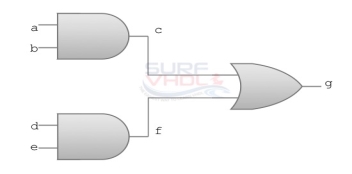
This can be shown with the help of an example:
Logic gates
use IEEE.STD_LOGIC_1164.ALL;
use IEEE.STD_LOGIC_ARITH.ALL;
use IEEE.STD_LOGIC_UNSIGNED.ALL;
entity and_or is
port (
a: in std_logic;
b: in std_logic;
d: in std_logic;
e: in std_logic;
g: out std_logic);
end and_or;
architecture and_or_a of and_or is
-- declarative part: empty
begin
g <= (a and b) or (d and e);
end and_or_a;
Multiplexers
use IEEE.STD_LOGIC_1164.ALL;
use IEEE.STD_LOGIC_ARITH.ALL;
use IEEE.STD_LOGIC_UNSIGNED.ALL;
entity MUX_SOURCE is
Port (S: in STD_LOGIC_VECTOR (1 downto 0);
I: in STD_LOGIC_VECTOR (3 downto 0);
Y: out STD_LOGIC);
end MUX_SOURCE;
architecture Behavioral of MUX_SOURCE is
begin
process (S, I)
begin
if (S <= "00") then
Y <= I (0);
elsif (S <= "01") then
Y <= I (1);
elsif (S <= "10") then
Y <= I (2);
else
Y <= I (3);
end if;
end process;
end Behavioral;
Subtractors
Write code for Half Subtractor
library IEEE;
use IEEE.STD_LOGIC_1164.ALL;
entity half_sub is
port (a, b: in std_logic;
dif, bo: out std_logic
);
end half_sub;
architecture sub_arch of half_sub is
begin
dif <= a xor b;
bo <= (not a) and b;
end sub_arch;
Adders
library IEEE;
use IEEE.STD_LOGIC_1164.ALL;
use IEEE.STD_LOGIC_ARITH.ALL;
use IEEE.STD_LOGIC_UNSIGNED.ALL;
entity FULLADDER_BEHAVIORAL_SOURCE is
Port (A: in STD_LOGIC_VECTOR (2 downto 0);
O: out STD_LOGIC_VECTOR (1 downto 0));
end FULLADDER_BEHAVIORAL_SOURCE;
architecture Behavioral of FULLADDER_BEHAVIORAL_SOURCE is
begin
process (A)
begin
—for SUM
if (A = “001” or A = “010” or A = “100” or A = “111”) then
O (1) <= ‘1’;
—single inverted commas used for assigning to one bit
else
O (1) < = ‘0’;
end if;
—for CARRY
if (A = “011” or A = “101” or A = “110” or A = “111”) then
O (0) <= ‘1’;
else
O (0) <<= ‘0’;
end if;
end process;
end Behavioral;
Flip-Flops
Write a code for JK flip-flop.
library IEEE;
use IEEE.STD_LOGIC_1164.all;
entity jk is
port (
j: in STD_LOGIC;
k: in STD_LOGIC;
clk: in STD_LOGIC;
reset: in STD_LOGIC;
q: out STD_LOGIC;
qb: out STD_LOGIC
);
end jk;
architecture jk_flip_flop of jk is
begin
jkff: process (j, k, clk, reset) is
variable m: std_logic: = '0';
begin
if (reset='1') then
m: = '0';
elsif (rising_edge (clk)) then
if (j/=k) then
m: = j;
elsif (j='1' and k='1') then
m: = not m;
end if;
end if;
q <= m;
qb <= not m;
end process jkff;
end jk_flip_flop;
library IEEE;
use IEEE.STD_LOGIC_1164.all;
entity SR_Latch is
port (
enable: in STD_LOGIC;
s: in STD_LOGIC;
r: in STD_LOGIC;
reset: in STD_LOGIC;
q: out STD_LOGIC;
qb: out STD_LOGIC);
end SR_Latch;
architecture SR_Latch_arc of SR_Latch is
begin
latch: process (s, r, enable, reset) is
begin
if (reset='1') then
q <= '0';
qb <= '1';
elsif (enable='1') then
if (s/=r) then
q <= s;
qb <= r;
elsif (s='1' and r='1') then
q <= 'Z';
qb <= 'Z';
end if;
end if;
end process latch;
end SR_Latch_arc;
Comparator
Write a program for 1-bit comparator
use IEEE.STD_LOGIC_1164.ALL;
entity comparator_1bit is
Port (A, B: in std_logic;
G, S, E: out std_logic);
end comparator_1bit;
architecture comp_arch of comparator_1bit is
begin
G <= A and (not B);
S <= (not A) and B;
E <= A xnor B;
end comp_arch;
Write a program for 8-bit comparator
library IEEE;
use IEEE.STD_LOGIC_1164.ALL;
entity comparator_8bit is
Port (A, B: in std_logic_vector (0 to 7);
G, S, E: out std_logic);
end comparator_8bit;
architecture comp_arch of comparator_8bit is
begin
process
begin
if A=B then
G <= ‘0’;
S <= ‘0’;
E <= ‘1’;
elsif A>B then
G <= ‘1’;
S <= ‘0’;
E <= ‘0’;
elsif A<B then
G <= ‘0’;
S <= ‘1’;
E <= ‘0’;
end if;
end process;
end comp_arch;
Decoder
Write a program for 3:8 Decoder
Counter
Write program for 4-bit binary counter
use IEEE.STD_LOGIC_1164.ALL;
use IEEE.STD_LOGIC_ARITH.all;
use IEEE.STD_LOGIC_UNSIGNED.all;
entity counter is
Port (rst, clk: in std_logic;
o: out std_logic_vector (0 to 3));
end counter;
architecture count_arch of counter is
signal count: std_logic_vector (0 to 3);
begin
process (rst, clk)
begin
if (rst = ‘1’) then count <= “0000”;
elsif (clk ’event and clk = ‘1’) then count <= count + 1;
end if;
end process;
o <= count;
end count_arch;
Write VHDL code for 4-bit synchronous up/down counter with asynchronous active-low reset
library ieee;
use ieee.std_logic_1164.all;
entity my_bcd_ud_count is
port (clock, resetn, ud: in std_logic;
Q: out integer range 0 to 15);
end my_bcd_ud_count;
architecture bhv of my_bcd_ud_count is
signal Qt: integer range 0 to 15;
begin
process (resetn, clock, ud)
begin
if resetn = '0' then
Qt <= 0;
elsif (clock ‘event and clock='1') then
if ud = '0' then
Qt <= Qt - 1;
else
Qt <= Qt + 1;
end if;
end if;
end process;
Q <= Qt;
end bhv;
Shift Register
Write VHDL code for Parallel in Parallel Out Shift Register
library ieee;
use ieee.std_logic_1164.all;
entity pipo is
port (
clk: in std_logic;
D: in std_logic_vector (3 downto 0);
Q: out std_logic_vector (3 downto 0)
);
end pipo;
architecture arch of pipo is
begin
process (clk)
begin
if (CLK ‘event and CLK='1') then
Q <= D;
end if;
end process;
end arch;
Write VHDL Code for Serial In Parallel Out Shift Register
library ieee;
use ieee.std_logic_1164.all;
entity sipo is
port (
clk, clear: in std_logic;
Input_Data: in std_logic;
Q: out std_logic_vector (3 downto 0));
end sipo;
architecture arch of sipo is
begin
process (clk)
begin
if clear = '1' then
Q <= "0000";
elsif (CLK ‘event and CLK='1') then
Q (3 downto 1) <= Q (2 downto 0);
Q (0) <= Input_Data;
end if;
end process;
end arch;
Write VHDL code for 8-bit register with enable and asynchronous reset
library ieee;
use ieee.std_logic_1164.all;
entity reg8 is port (clock, resetn, E: in std_logic;
D: in std_logic_vector (7 downto 0);
Q: out std_logic_vector (7 downto 0));
end reg8;
architecture bhv of reg8 is
begin
process (resetn, E, clock)
begin
if resetn = '0' then
Q <= (others => '0');
elsif (clock ‘event and clock = '1') then
if E = '1' then
Q <= D;
end if;
end if;
end process;
end bhv;
Write VHDL code for 8-bit register with enable and asynchronous reset
library ieee;
use ieee.std_logic_1164.all;
entity my_rege is
generic (N: INTEGER: = 4);
port (clock, resetn: in std_logic;
E, sclr: in std_logic;
D: in std_logic_vector (N-1 downto 0);
Q: out std_logic_vector (N-1 downto 0));
end my_rege;
architecture Behavioral of my_rege is
signal Qt: std_logic_vector (N-1 downto 0);
begin
process (resetn, clock)
begin
if resetn = '0' then Qt <= (others => '0');
elsif (clock ‘event and clock = '1') then
if E = '1' then
if sclr='1' then Qt <= (others =>'0');
else Qt <= D;
end if;
end if;
end if;
end process;
Q <= Qt;
end Behavioral;
References:
S. Widemer and Gregory L. Moss, Pearson Education.
6. A First Course in Digital System Design: An Integrated Approach, India Edition, John P. Uyemura, PWS Publishing Company, a division of Thomson Learning Inc.
7. Digital Systems – Principles and Applications, 10th Edition, Ronald J. Tocci, Neal
S. Widemer and Gregory L. Moss, Pearson Education.