Unit-5
Power Converters
n-Type semiconductors
To increase the number of conduction band electrons intrinsic silicon, pentavalent imparity atoms are added. These are atoms with five valence electrons such as
i) arsenic (As)
Ii) phosphors (P)
Iii) Bismuth (Bi)
Iii) Antimony (Sb)
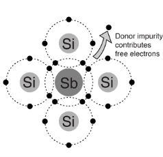
- Pentavalent impurity atom in a silicon crystal. An antimony (sb) impurity atom shown above-
- Each pentavalent atom forms covalent bonds with four adjustment silicon atoms, leaving one extra electron.
- The pentavalent atom gives up on electron, it often called a donor atom.
- Majority and minority carriers: A type here mean negative charge of an electron. Electrons are called the majority carriers in n-type material.
- Hole in an n-type material are called minority carriers
p-Type semiconductors
To increase the number of holes in intrinsic silicon, trivalent impurity atoms are added. These are atoms with three valence electrons such as
i) Boron(B)
Ii) Indium(In)
Iii)Gallium(Ga)
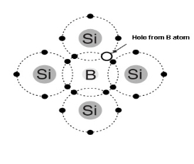
- Trivalent impurity atom in a silicon crystal structure. A) boron (B) impurity atom is shown in the center.
- The number of holes can be carefully controlled by the number of trivalent impurity atoms added to the silicon.
- A Hole created by the doping process is not accompanied by a conduction (free)electron.
- Trivalent Atom can take an electron it is often referred to as on accepted atom
Semiconductor conductivity
The conductivity of a material depends upon the concentration of free electrons. In semiconductors the concentration of electrons is in between conductors and insulators. As discussed in earlier section that the conduction in semiconductor is possible up to some temperature. Germanium and silicon are generally used semiconductors. If we talk about Ge than it has 4 electrons in its outer most shell which can form covalent bond with four adjacent Ge atoms.
At absolute zero the semiconductors behave as insulators as there are no free electrons for conduction. At room temperature due to presence of some energy few covalent bonds break and there are some free electrons. These free electrons contribute in conduction. For Ge the energy required to break the covalent bond is 0.72eV. For Si the energy required to break the covalent bond is 1.1eV at room temperature.
In semiconductors the holes can also be considered as the carrier of electricity. The hole exists in semiconductors where there is incomplete bond. When an electron leaves its place and to form bond with neighbouring atom it creates a new hole at that place. This process continues as every time due to electrons a new hole is created. So, it can be visualized as the holes move in opposite direction to the electrons. In ideal case the semiconductor has equal number of holes and electrons.
The current density due to drift holes for applied field E is given as
Jh=q p pE
pE
The current density due to drift electrons for applied field E is given as
Je = q pn n E
n E
The drift current density is given as
J= Jp+Jn
J = q (p p+n
p+n n) E
n) E
J= E
E
 =q (p
=q (p p+n
p+n n)
n)
Where
 = Conductivity of semiconductors
n, p = magnitude of free electron and hole concentration respectively.
Q1) For a p-type Ge ni = 2.1x10¹⁹m-3 density of boron =3.2x10²³ atoms m-3. The electron and hole mobility are 0.4 and 0.2 m2V-1s-1. Calculate conductivity before and after addition of boron?
Sol: Before adding boron
 =q (p
=q (p p+n
p+n n)
n)
= ni q ( p+
p+ n) = 2.1x1019x1.6x10-19x(0.4+0.2)=2.016 S/m-1
After adding boron
 =q p
=q p p
p
= 3.2x1023x1.6x10-19x0.2=10.24x10³S/m-1
Q1) Determine the density of the donor atoms which have been added to the intrinsic Ge to make it a n-type material of resistivity 0.1x10⁻²ohm-m. Mobility of electron in n-type semiconductor is 0.5m2V-1s-1.
Sol:  =q (n
=q (n n)
n)
n=  /q
/q n
n
 = 1/
= 1/
n= 1/ q
q n = 1/(0.1x10-2x0.5x1.6x10-19) = 1.25x10²²m-3
Q2) The intrinsic carrier density at room temperature in Ge is 3.4x10¹⁹m-3. If electron and hole mobilities are 0.4 and 0.2 m2V-1s-1 respectively. Calculate its resistivity?
Sol:  = 1/
= 1/
 =ni q (
 p+
p+ n) = 3.4x1019x 1.6x10-19(0.4+0.2) = 3.264S/m-1
 = 1/
= 1/ = 1/3.264 = 0.31ohm-m
Q3) The electron and hole mobilities in In-Sb are 6 and 0.2m2V-1s-1 respectively. At room temperature resistivity of In-Sb is 2x10⁻⁴ohm-m. Find intrinsic carrier concentration assuming the material to be intrinsic?
Sol:  = 1/
= 1/
 =ni q (
 p+
p+ n)
n)
ni = 1/ q (
q ( p+
p+ n) = 1/2x10-4x1.6x10-19(6+0.2) = 5.04x10²¹m-3
Q4) An electric field of 90Vm-1 is applied to n-type semiconductor. Determine the current density in sample given electron mobility 0.4m2V-1s-1, n=5.9x10²⁰m-3?
Sol: J= E
E
 = nq
= nq n = 5.9x1020x1.6x10-19x0.4=37.36S/m-1
J=3.39x10³
Q5) Determine the density of the donor atoms which have been added to the intrinsic Ge to make it a n-type material of resistivity 0.5x10⁻²ohm-m. Mobility of electron in n-type semiconductor is 0.8m2V-1s-1.
Sol:  =q (n
=q (n n)
n)
n=  /q
/q n
n
 = 1/
= 1/
n= 1/ q
q n = 1/(0.5x10-2x0.8x1.6x10-19) = 1.56x10²¹m-3
PN Junction:
When a semi-conductor is doped such that half the portion is doped with the trivalent impurity (Al, Ar, Bi) and the other half is doped with pentavalent impurity (B, P) then the junction formed is known as PN junction.

Its symbol is

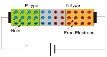
Forward Biased P-N Junction
When p-type region is connected with the positive terminal and n-type region with the negative terminal of the voltage source, then the junction is said to be forward biased.
At this condition, due to the attraction of cathode, electrons create covalent bond in p-type material and are attracted towards the terminal.
Hence, numbers of covalent bonds are broken and electrons moves towards the positive terminal increasing the concentration of electrons in the crystal nearer to the terminal and these electrons recombine with holes here.
In this way, the number of holes increases in the p-type region away from the junction, and it is reduced in the portion of p-type region nearer to the terminal.
Due to the higher concentration of holes adjacent to negative impurity ions layer the electrons of negative ions come out and recombine with those holes and create new holes in the layer.
Consequently, the width of this negative ions layer is reduced and finally this layer vanishes.
Reverse Biased PN Junction
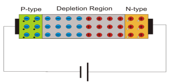
When positive terminal is connected to the n-type region and the negative terminal is connected to the p-type region then the pn junction is said to be in reverse biased condition.
When no voltage applied across the p n junction, the potential developed across the junction is 0.3 volts at 25oC for germanium and 0.7 volts at 25oC for silicon p n junction.
The polarity of this potential barrier is same as the polarity of voltage source applied during reverse biased condition.
Now if reverse biased voltage is increased the barrier potential developed also increases. Hence, the pn junction widens.
The free electrons of the n-type region are attracted towards positive terminal of the source because of that more positive impurity ions are created in the depletion layer which makes the layer thicker.
At the same time, electrons are injected in the p-type region. Due to the positive potential of the n-type region the electrons are drifted towards the junction and combine with holes and create more positive impurity ions in the layer.
Key Takeaways:
- The free electrons from the negative terminal of the battery continue to pour into the n-region while the free electrons in the n-region move towards the junction.
- The electrons travel through the n-region as free electrons hence, current in n-region is by free electrons.
- When these electrons reach the junction, they combine with holes and become valence electrons.
- As valence electron, they move through the holes in the p-region, hence, current in the p-region is by holes.
- When these valence electrons reach the left end of the crystal, they flow into the positive terminal of the battery.
When the diode is not biased a natural potential barrier is developed across the depletion region which is of 0.5-0.7V for Si and 0.2-0.3V for Ge diodes.
When the diode is forward biased the thickness of depletion region reduces (VD>0) and the diode acts like a short circuit. There is large amount of current flowing due to this short circuit.
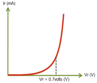
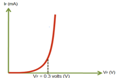
When the diode is reverse biased the thickness of depletion region increases (VD<0) and the diode acts as an open circuit. There is high voltage and no current dure to open circuit.
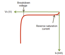
The diode current equation is given as
I=I0 ( – 1)
– 1)
I = diode current
I0 = Saturation current
Q=charge
V=Voltage applied across diode
K= Boltzmann constant=1.38x10⁻²³ JK-1
T= temperature in kelvin
For forward biased diode large amount of current flows so the above equation becomes
I=I0 ( )
)
As the current is large so 1 is neglected.
For reverse biased diode the exponential term is neglected so the current equation becomes
I=I0
BJT: The BJT is constructed with the three draped semiconductors region’s separate by two Pn junctions as shown below
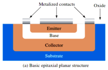
-Basic epitaxial planner structures.
-Three terminal with region’s are called emitter, base and collector.
-The physical representation of the two types of BJT’s,
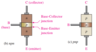
One type consists between two regions separated by a P region (npn) and other type consists of two p regions separated by an n region (pnp).
-The Pn junction joining the base region and the emitter region is called the base emitter junction.
-The Pn junction joining the base region and the collector region is called the base collector junction.
-The base region is lightly doped and very thin compared to the heavily doped emitter and the moderately doped collector regions.
Transistor Current:-
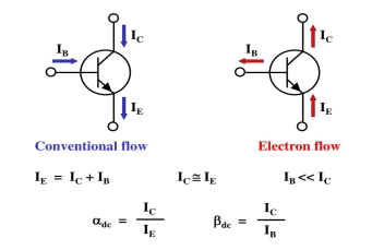
Transistor’s Characteristic’s and parameters:-
-The transistors is connected to d.c bias vtg for both the npn&pnp types VBB forward biases the base emitter junction &Vcc reverse biases the base collector junction.
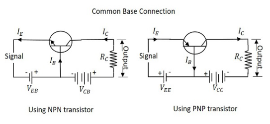
*Biasing conditions for different regions of operation:-
Sr. No | Region of operation | BE junction | CB junction | Work |
1 | Cutoff region | R.B | R.B | S/w |
2 | Active region | F.B | R.B | Ampr |
3 | Saturation region | F.B | F.B |
|
Transistor’s Configuration:-
1) Common Base configuration(C.B)
2) Common emitter Configuration(C.E)
3) Common Collector Configuration(C.C)
BJT Switching
Common Emitter (CE) configuration
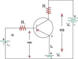
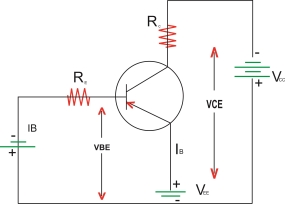
The important points about the CE
Configurations are as follows: the emitter acts as a common terminal between I/p and output. The /p Vtg. Is called between base and emitter
Hence VBE is the I/p Vtg. And IB is the input current.
The O/p is taken between the collector and emitter. There for VCE is the O/p Vtg. And IC is the O/p current.
In order to operate the transistor in its active region the base emitter (BE) junction is forward biased and collector base junction is reverse biased.
- Current relations in CE Configuration:
IE = IC + IB
Where IC =  d.c.IE + ICBO
Rearrange this eqn to get
IC – ICBO =  d.c.IE
 -
-  = IE = IC + IB
 ] = IB -
IC  ] = IB +
 ] +
] + 
- Current gain
 : as
: as  is the ration of o/p current TC and I/p current IB it called common emitter current amplification factor or simply current gain. Thus, transistor acts as current amplifier.
The value of  is match higher than
 =
= 
 =
=  =
=  =
= 
IC =  IB +
IB +  …….. I
But  =
= 
 1 +
1 +  =
=  + 1
+ 1
1 +  =
= 
 1 +
1 +  =
= 
Put in eqn I
IC =  IB + (1+
 ICBO above eqn can be expressed as
IC =  IB + ICEO
Where ICEO is the reverse saturation current for the CE configuration which is given by
ICEO = (1+  ) ICBO
- Reverse leakage current:
The Reverse leakage current of a transistor operating
In the LE configuration is denoted by
ICEO = (1 +  ) ICBO
As the value of 
- Match greater than 1 ICEO>>>> ICBO
- As IC =

Put IB = 0
 IC = (1 +
The Reverse leakage current (ICEO)
Increases with increase in the temperature this current flows in the same direction as that of IC there for the collector current IC will increase with increase in temperature even when IB is constant
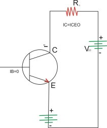
This is called as thermal instability so in CE configuration thermal stabilizing CKT must be included.
- Relation between IC and IB (Current gain
 )
)
We know that
IC 
Though ICEO is large it is much smaller as compared to . Therefor the eqn for IC gets modified as
 C =
C = 

- Relation betn
 &
& :
:
We know that
 but
but
 =
=  =
= 
 =
= 
Similarly we can obtain the expression for  d.c in terms of
  as follows
 d.c =
d.c =  but
but 
=
Multiply & divide numerator & denominator for by IE
 d.c =
d.c = 
 d.c =
d.c = 
 =
= 
- Impact characteristics:
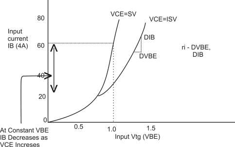
The value of dynamic input resistance ri is low for the CE configuration but it is not as low as that of CE configuration
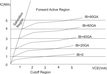
- Cutoff region: Both the BE & CB junctions are reverse biased to operate the transistor in cutoff region. The base current IB = 0 & the collector current is equal to the reverse leakage ICEO. The region below the characteristics for
IB = 0 is cutoff region.
- Active region: the BE emitter junction is forward biased CB junction is reverse biased to operate the transistor in the active region
The collector current IC increases slightly with increase in the vtg. VCE. However, the collector current is largely dependent on the base current IB
At fixed value of VCE if IB is increased then it will cause IC to increase substantially.
This is because IC = BIB this relation is true only for the active region of operation.
- Saturation region: the BE junction as well as the collector junction must be forward biased to operate the transistor in its saturation region
- Dynamic o/p resistance
 / constant IB
Q) In a CB IE= 2mA, IC=1.5mA. Calculate IB?
Sol: IE =IB+IC
2= IB+1.5
IB=0.5mA
Q) In a CB current amplification factor is 0.9. If emitter current is 1.2mA. Determine the value of base current?
Sol: α = 0.9
IE =1.2mA
α = IC/ IE
IC = α IE =0.9 x 1.2 = 1.08mA
IE =IB+IC
1.2= IB+1.08
IB= 0.12mA
Q) In a CB connection IC=1.0mA and IB= 0.02mA. Find the value of current amplification factor?
Sol: IE =IB+IC =1+0.02 = 1.02mA
α = IC/ IE
α = 1.0/1.02 = 0.98
Q) In a CB connection the emitter current is 0.98mA. If the emitter circuit is open the collector current becomes 40 A. Find total collector current. α =0.92
Sol: ICBO=40 A
A
IC =α IE+ICBO
= (0.92 x 0.98x10-3) + 40x10-6
IC =0.94mA
Q) In a common base connection, α = 0.95. The voltage drop across 3 kΩ resistance which is connected in the collector is 2.5 V. Find the base current.
Sol: IC = 2.5/3000 = 0.83mA
α = IC/ IE
IE = IC/α =0.83/0.95=0.87mA
IE =IB+IC
0.87 =IB+0.83
IB=0.04mA
Q) Find the value of β if (i) α = 0.9 (ii) α = 0.98 (iii) α = 0.99.
Sol:  = α/1- α = 0.9/1-0.9 = 9
 = α/1- α = 0.98/1-0.98 = 49
 = α/1- α = 0.99/1-0.99 = 99
Q) The collector leakage current in a transistor is 200 μA in CE arrangement. If nowthe transistor is connected in CB arrangement, what will be the leakage current? Given that β = 120.
Sol: ICEO=200 μA
 = 120
= 120
α = /1+
/1+ = 120/121=0.99
ICEO=ICBO/1- α
ICBO= 1.6μA
Q) For a certain transistor, IB = 18 μA; IC = 2 mA and β = 60. Calculate ICBO.
Sol: IC =  IB+ICEO
ICEO=IC -  IB= 2x10⁻³-(60x18x10-6) = 0.92mA
α = /1+
/1+ = 60/61=0.98
ICBO= (1- α)ICEO = (1-0.98) x 0.92=15.08 μA
The thyristor has four-layer p-n-p-n with three junctions. The three terminals are anode, cathode and the gate. The circuit diagram is shown below
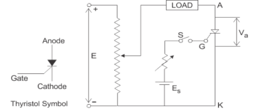
As we can see from above circuit diagram anode and cathode are connected to supply voltage. The gate and cathode are connected to supply Es. The V-I characteristics are shown below.
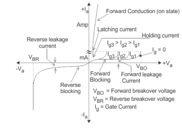
The thyristor operates in three modes
i) Reverse Blocking Mode: In this mode cathode is more positive than the anode by voltage E. The supply Es is initially detached and switch S is kept open. In this case J1 and J3 are reversed biased and J2 are forward biased.
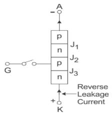
The reverse voltage is increased than at particular voltage VBR avalanche occurs at J1 and J3 and reverse current increases. This current causes more losses in SCR and increases heat in the circuit. So, the reverse voltage should not be increased more than VBR. When voltage is less than VBR the device has high impedance in reverse direction.
Ii) Forward Blocking Mode: The gate is open anode is positive in this case. The J1 and J3 are forward biased and J2 is reversed biased. A small forward leakage current flow. The current flows from anode to cathode. A thyristor is brought from forward blocking mode to forward conduction mode by turning it on by exceeding the forward break over voltage or by applying a gate pulse between gate and cathode. In this mode, thyristor is in on-state and behaves like a closed switch. The junction J2 which is reversed biased has an avalanche breakdown at voltage VB0. The thyristor operates as an open switch during forward blocking mode.
Iii) Forward Conduction Mode: When the forward voltage anode to cathode voltage is increased keeping gate open the junction J2 has avalanche breakdown at VBO making thyristor ON.The thyristor conducts maximum current with minimum voltage drop, this is known as the forward conduction forward conduction or the turn on mode of the thyristor.
Power transistor
They have controlled characteristics and are turned on when current is given to base. The transistor remains in ON state as long as control signal is present. There are two types of power transistors
i) BJT: Refer section 5.2
Ii) MOSFET:
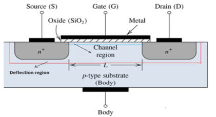
The MOSFET (Metal Oxide Semiconductor Field Effect Transistor) transistor is a semiconductor device which is widely used for switching and amplifying electronic signals in the electronic devices.
It is a core of integrated circuit and is designed and fabricated in a single chip because of its small size.It is a four terminal device with source(S), gate (G), drain (D) and body (B) terminals.The body of the MOSFET is connected to the source hence making it a three terminal device like field effect transistor. It can be used in both analog and digital circuits.
Operation
The MOSFET works by electronically varying the width of a channel along which charge carriers flow (electrons or holes).
The charge carriers enter the channel through source and exit via the drain.
The width of the channel is controlled by the gate voltage which is located between source and drain.
It is insulated from the channel near an extremely thin layer of metal oxide.
Function:
- Depletion Mode
When there is no voltage on the gate, the channel shows maximum conductance. When the voltage on the gate is either positive or negative, the channel conductivity decreases.
2. Enhancement Mode
The device does not conduct when there is no voltage on the gate. As the voltage increases on the gate, the better the device can conduct.
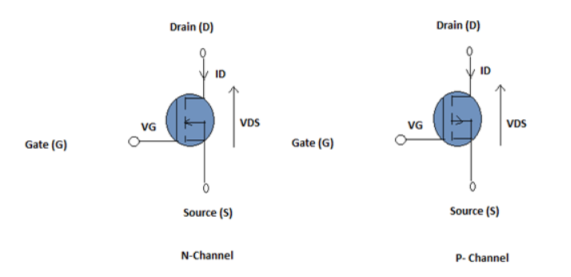
Working:
The aim of the MOSFET is to be able to control the voltage and current flow between the source and drain. It works like a switch.
The working depends upon the MOS capacitor.
The MOS capacitor is the main part of MOSFET.
The semiconductor surface at the below oxide layer is located between source and drain terminal. It can be inverted from p-type to n-type by applying positive or negative gate voltages respectively.
When the positive gate voltage is applied, the holes present under the oxide layer repel with a repulsive force and holes are pushed downward with the substrate.
The depletion region populated by the negative charges is the acceptor atoms. The positive voltage also attracts electrons. Now, if a voltage is applied between the drain and source, the current flows between the source and drain and the gate voltage controls the electrons in the channel.
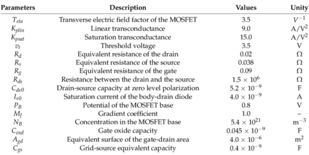
MOSFET parameters
IGBT (Insulated Gate Bipolar Junction Transistor):
This device has advantages of both BJT and MOSFET. It has high input impedance like MOSFET and low on state power loss like BJT. The major difference between MOSFET and IGBT is the substrate. The n+ layer substrate at drain in MOSFET is substituted by p+ layer substrate at collector.
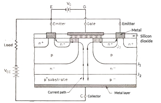
When the gate is positive with respect to the emitter and with G-E voltage more than the threshold voltage of IGBT an n-channel is formed in the p-region shown in above figure. The n-channel short circuits the n- and n+ emitter regions. The electron movement in n-channel causes substantial hole injection from p+ substrate layer into the epitaxial n- layer establishing the forward current. The three layers p+, n- and p form pnp transistor with p+ emitter n- as base and p as collector.
IGBT Characteristics
The n-channel type IGBT characteristics are shown below. The ICcollector current is plotted for various value of VCE for various values of VGE. For forward biased the characteristics are similar to that of a BJT. The controlling parameter here is VGE because IGBT is a voltage-controlled device.
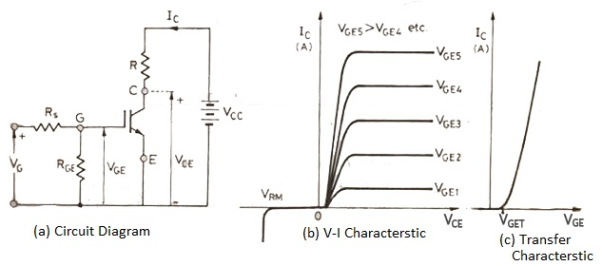
The transfer characteristics shows IC varied according to the VGE. These are similar to the MOSFET. The IGBT is OFF when VGE is less than threshold voltage VGET. During OFF state the junction J2 blocks forward voltage and in case reverse voltage appears across collector and emitter junction J1 blocks it.
The word rectification means converting an oscillating AC voltage into a constant current DC. This can be achieved by using thyristors, diodes, transistors or converters. The single-phase rectifier can be of two types
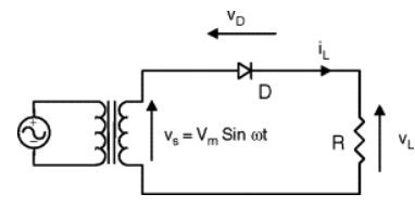
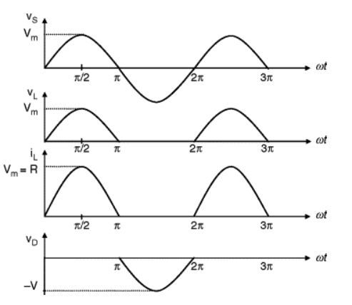
i) half wave rectifier: The circuit for half wave rectifier is shown below. The input is a sinusoidal wave. During the positive half cycle the diode is forward biased and hence it conducts (ON State) and voltage drop is across the load which is resistive load. During the negative half cycle the diode is reversed biased (OFF State) and hence there is no current in the circuit.
Ii) Full wave rectifier: In this case there are four thyristors used out of these four two are conducting in each half cycle. The circuit diagram is shown below.
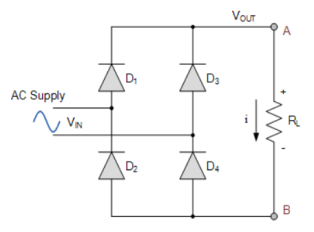
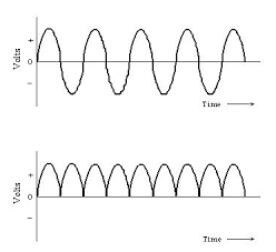
During positive half cycle D1 and D4 are forward biased and D2 and D3 are reverse biased. The current flows through path D1-A-RL-B-D4 and back to supply.
During positive half cycle D2 and D3 are forward biased and D1 and D4are reverse biased. The current flows through path D3-A-RL-B-D2 and back to supply.
Q) A single-phase half-wave rectifier is connected to a 50V RMS 50Hz AC supply. If the rectifier is used to supply a resistive load of 150 Ohms. Calculate the equivalent DC voltage developed across the load, the load current and power dissipated by the load. Assume ideal diode characteristics.
Sol: Maximum Voltage Amplitude, VM
VM = 1.414*VRMS = 1.414*50 = 70.7 volts
b) Equivalent DC Voltage, VDC
VDC = 0.318*VM = 0.318*70.7 = 22.5 volts
c) Load Current, IL
IL = VDC /RL = 22.5/150 = 150mA
d) Power Dissipated by the Load, PL
PL = V*I or I2*RL = 22.5*0.15 = 3.4W
Q2) Four diodes are used to construct a single phase full-wave bridge rectifier circuit which is required to supply a purely resistive load of 2kΩ at 240 volts DC. Calculate the RMS value of the input voltage required, the total load current drawn from the supply, the load current passed by each diode and the total power dissipated by the load. Assume ideal diode characteristics.
Sol: Rectifier Supply Voltage, VRMS
VDC = 0.9*VRMS
VRMS = VDC/0.9 = 220/0.9 = 244.4 VRMS
b) Load Current, IL
IL = VDC/ RL = 240/1000 =120mA
c) Load Current Passed by Each Diode, ID
The load current is supplied by two diodes per cycle, thus:
ID = IL/2 = 0.12/2 =60mA
d) Power Dissipated by the Load, PL
PL = V*I or I2*RL = 240*0.12 = 28.8W
The device which converts DC voltage into AC voltage is called as inverter. The single-phase inverter is of two types
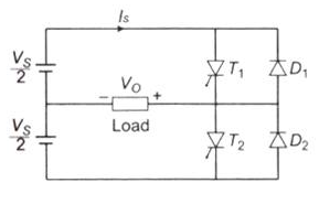
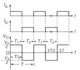
i) Half-Bridge Inverter: The circuit has two thyristors and two diodes and a resistive load as shown below. The thyristor T1 and T2 are connected with feedback diodes D1 and D2. When T1 is ON and T2 is OFF the current flows through Vs/2-T1-Vs/2. It conducts in positive half cycle. When T2 is ON and T1 is OFF the current flows through Vs/2-T2-Vs/2. It conducts in negative half cycle.
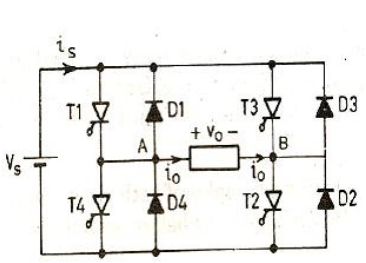
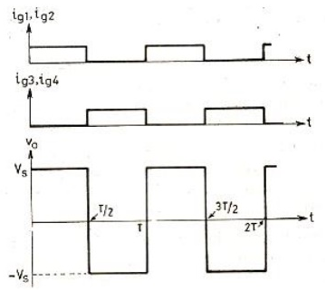
Ii) Full-Bridge Inverter: In a full-bridge inverter, four thyristors and four feedback diodes used with D source voltage. In mode-1 T1 and T2 are ON and T3 and T4 are OFF. The current flows from Vs-T1-A-RL-B-T2-Vs. The current flows from A-B through load generating positive half cycle.
In mode-1 T3 and T4 are ON and T1 and T2 are OFF. The current flows from Vs-T3-B-RL-A-T4-Vs. The current flows from B-A through load generating negative half cycle.
DC-DC Buck and Boost Converters
It is basically a DC-DC converter which has output either low or high than the input voltage value. It is combination of a step up (Buck) and step up (Boost) converter. These devices have a diode connected with inductor and a capacitor. The input is connected to a solid-state device. The diode acts as a switch. The circuit shown below is of a buck-boost converter.

Fig: Buck-Boost Converter
The diode is in the reverse direction to the source. The capacitor and diode are in parallel to load. We use pulse width modulation to turn the controlled switch ON and OFF. Normally time based PWM is used as frequency based is difficult in implementation. This operates in two modes
i) When switch is ON, Diode is OFF: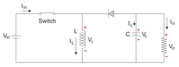
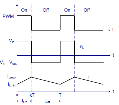
As seen from the above figure when the switch is ON it acts as a short circuit and hence, allows all the current to pass through it. In this condition the current flows through the switch and inductor and again to the input. The inductor stores energy at this time. When the switch is OFF the inductor reverses its polarity and then the current flows through the load and then diode and back to the inductor.
The total time period T = TON+TOFF
TON: ON time
TOFF: OFF time
The switching frequency fs= 1/T
In steady state Vin=VL
VL= L  = Vin
= Vin
Now duty cycle D= 
 =
= 
At end of ON state
 ILON =
  =
=  dt =
dt = 
Ii) When switch is OFF, Diode is ON:
The circuit is shown below where the switch is in OFF state. The polarity of inductor is reversed. The current flows through the load resistance from the inductor and a step-up voltage is obtained at the output.
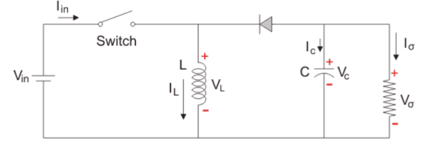
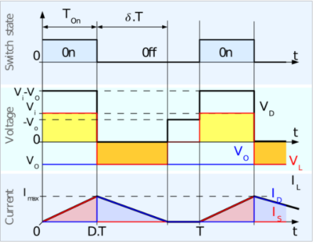
In this case VL=Vo
VL= L  = Vo
= Vo
 =
= 
TOFF= T-TON = T_DT = (1-D) T
 t= (1-D) T
 iL)open=
  (1-D) T
Duty ratio control
It is the period for which the signal is active. The time the signal takes to complete one cycle is called as period.
D= PW/T x 100%
D: Duty cycle
PW: pulse width
T: total period of signal
Reference
1 D.P Kothari and I.J Nagrath “Basic electrical engineering” Tata Mcgraw Hill,2010
2 D.C.Kulshtreshtha Basic electrical engineering” Tata Mcgraw Hill,2009
3 E.Hughes “Electrical and Electronics Technology” Pearson,2010
4 V.D.Toro “Electrical Engineering Fundamentals” Prentice Hall India, 1989