UNIT 8
Basics of Electronics
Basic amplifier
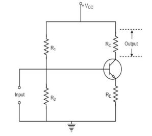
When a weak input signal is given to the base of the transistor as shown in the figure, a small amount of base current flows.
Due to the transistor action, a larger current flow in the collector of the transistor. Now, as the collector current increases, the voltage drop across the resistor RC also increases, which is collected as the output.
Hence a small input at the base gets amplified as the signal of larger magnitude and strength at the collector output. Hence this transistor acts as an amplifier.
Biasing Circuit
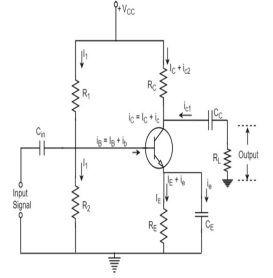
The resistors R1, R2 and RE form the biasing and stabilization circuit, which helps in establishing a proper operating point.
Input Capacitor Cin
This capacitor couples the input signal to the base of the transistor. The input capacitor Cin allows AC signal,but isolates the signal source from R2. If this capacitor is not present, the input signal gets directly applied, which changes the bias at R2.
Coupling Capacitor CC
This capacitor is present at the end of one stage and connects it to the other stage. As it couples two stages it is called as coupling capacitor. This capacitor blocks DC of one stage to enter the other but allows AC to pass. Hence it is also called as blocking capacitor.
Emitter by-pass capacitor CE
This capacitor is employed in parallel to the emitter resistor RE. The amplified AC signal is by passed through this. If this is not present, that signal will pass through RE which produces a voltage drop across RE that will feedback the input signal reducing the output voltage.
The Load resistor RL
The resistance RL connected at the output is known as Load resistor. When a number of stages are used, then RL represents the input resistance of the next stage.
Circuit currents
Base Current
When no signal is applied in the base circuit, DC base current IB flows due to biasing circuit. When AC signal is applied, AC base current ib also flows. Therefore, with the application of signal, total base current iB is given by
iB=IB+I b
Collector Current
When no signal is applied, a DC collector current IC flows due to biasing circuit. When AC signal is applied, AC collector current ic also flows. Therefore, the total collector current iC is given by
iC=IC+ic
Where
IC=βIB= zero signal collector current
Ic=βib = collector current due to signal
Emitter Current
When no signal is applied, a DC emitter current IE flows. With the application of signal, total emitter current iE is given by
iE=IE+ie
Note that
IE=IB+IC
Ie=ib+ic
As base current is usually small,
IE≅IC and ie≅ic
Voltage:
Amplifier gain of an input signal:

Voltage amplifier gain:
Voltage gain (Av) = Output voltage / Input Voltage = V out/Vin
Current amplifier gain (Ai) = Output current /Input current
Power Amplifier gain
Power Gain (Ap) = Av x Ai
Basic Attenuators:
Signals are sent from one place to another through a medium. These signals can be data signals, voltage signals, current signals, etc. When the distance travelled by the signal increases the strength of the signal gradually decreases. This gradual loss of intensity of signals through the medium is called Attenuation.
The device which is designed to reduce the power of signals without disturbing its waveform is called as “Attenuator”.
The attenuator is highly used after signal generator circuits. It helps in attenuating or reducing the strength of high-level signals before applying them to the Antenna circuits.
An attenuator is a two-port electronic device It is designed using resistors to weaken or attenuate a signal. Attenuators are passive circuits, they work without any power supply.
These are available both as fixed attenuator with a fixed attenuation level and as a continuously changing attenuator. Contrary to amplifiers gain percentage, attenuator gives loss percentage. The amount of attenuation is measured in decibels.
CRO
The cathode ray oscilloscope is an electronic test instrument, it is used to obtain waveforms when the different input signals are given.
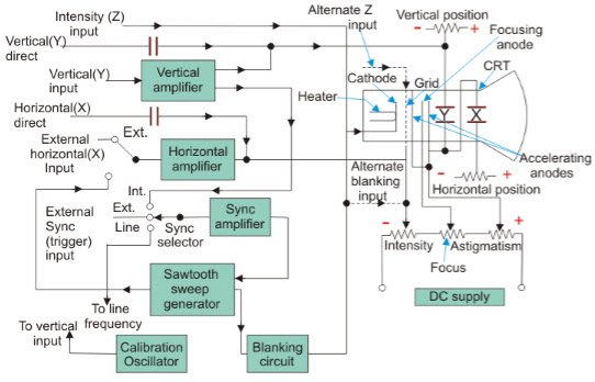
The following circuit diagram shows the basic circuit of a cathode ray oscilloscope. In this, we will discuss important parts of the oscilloscope.
Working of CRO
Vertical Deflection System
The main function of this amplifier is tamplify the weak signal so that the amplified signal can produce the desired signal. To examine the input signals are penetrated to the vertical deflection plates through the input attenuator and number of amplifier stages.
Horizontal Deflection System
The vertical and horizontal system consists of horizontal amplifiers to amplify the weak input signals, but it is different to the vertical deflection system. The horizontal deflection plates are penetrated by a sweep voltage that gives a time base. By seeing the circuit diagram the sawtooth sweep generator is triggered by the synchronizing amplifier while the sweep selector switches in the internal position. So, the trigger saw tooth generator gives the input to the horizontal amplifier by following the mechanism.
Recurrent Sweep
As the name, itself says that the saw tooth is respective that is a new sweep is started immodestly at the end of the previous sweep.
Triggered Sweep
Sometimes the waveform should be observed that it may not be predicted, thus the desired that the sweep circuit remains inoperative and the sweep should be initiated by the waveform under the examination. In these cases, we will use the triggered sweep.
Driven Sweep
In general, the drive sweep is used when the sweep is a free running but it is a triggered by the signal under the test.
Non-Saw Tooth Sweep
This sweep is used to find the difference between the two voltages. By using the non-sawtooth sweep we can compare the frequency of the input voltages.
Synchronization
The synchronization is done to produce the stationary pattern. The synchronization is between the sweep and the signal should measure. There are some sources of synchronization which can be selected by the synchronization selector. Which are discussed below.
Internal
In this the signal is measured by the vertical amplifier and the trigger is abstained by the signal.
External
In the external trigger, the external trigger should be present.
Line
The line trigger is produced by the power supply.
Intensity Modulation
This modulation is produced by inserting the signal between the ground and cathode. This modulation causes by brightening the display.
Positioning Control
By applying the small independent internal direct voltage source to the detecting plates through the potentiometer the position can be controlled and also we can control the position of the signal.
Intensity Control
The intensity has a difference by changing the grid potential with respect to the cathode.
Applications of CRO
- Voltage measurement
- Current measurement
- Examination of waveform
- Measurement of phase and frequency
Analog and digital signals
Analog Transmission
An analogue signal (otherwise known as a wave form) is characterised by being continuously variable along both amplitude and frequency. In the case of telephony, when we speak into a handset, our voice is converted into current, or voltage fluctuations. Those fluctuations in current are an analogue transmission of the actual voice pattern.
To transmit an analogue signal effectively, we need to define the frequency in which is operates. In telephony, the usable voice frequency band ranges from approximately 300 Hz to 3400 Hz, and so the network provider (phone company) will allocate a bandwidth of around 4,000Hz for voice transmission.
Because of the limited bandwidth analogue facilities have, they cannot support high-speed data transmission.
Digital Transmission
Digital signals are much simpler than analogue signals. Instead of a continuous wave form, analogue signals are made up of a series of pulses that represent either one bit or zero bits. Each computer system uses a coding scheme which defines what combinations of ones and zeros make up all the characters in the character set.
The data (ones and zeros) are carried throughout the network depending on whether it is an electrical or optical transmission system.
Bandwidth
Bandwidth is measured as the amount of data that can be transferred from one point to another within a network in a specific amount of time. Typically, bandwidth is expressed as a bitrate and measured in bits per second (bps).

The term bandwidth refers to the transmission capacity of a connection and is an important factor when determining the quality and speed of a network or the internet connection.
Modulation and demodulation
Modulation:
Modulation is defined as a process by which some characteristics or property of high frequency sine wave called the carrier signal is varied in accordance with the instantaneous amplitude of the message signal called modulating signal.
A sine wave carrier which is a high frequency signal may be represented by the signal
Vc = Vc sin(wct + ɸ) ----------------------------(1)
Where vc = instantaneous value of the carrier
Vc = peak or maximum amplitude of the carrier
Wc = angular frequency of the carrier
ɸ= phase angle of the carrier with respect to some reference.
Demodulation
Demodulation is defined as extracting the original information-carrying signal from a modulated carrier wave. A demodulator is an electronic circuit that is mainly used to recover the information content from the modulated carrier wave. There are different types of modulation and so are demodulators. The output signal via a demodulator may describe the sound, images, or binary data.
Filters
Filter: A filter is network which suppress certain range of frequencies and pass other frequencies without any loss of signal .
•Different types of filter bases on components used ;
• Active Filter.
• Passive filter
Different types of Filter based on frequency characteristics ;
• Low pass filter.
• High pass filter.
• Band pass filter.
• Band stop filter.
Low pass filter (LPF) : A filter that allows all the frequencies up to cut- off frequency to pass through it without attenuation is called LPF.
A LPF attenuates all the frequencies above the cut- off frequency.
High pass filter (HPF) : A filter which attenuates all the frequencies below a specified Frequency (fc) and passes all the frequencies above fc is called high pass filter.
Band Pass Filter (BPF) : A filter which allows all the frequencies below a specified cut off frequencies to pass and attenuates all the other frequencies is called Band Pass Filter (BPF).
Band Stop Filter (BSF) : A filter which allows all the frequencies between two specified cutt off frequencies and pass all other frequencies is called band stop filter (BSP).
Frequency Response: Variation of signal with frequency is called frequency response.
Forward biased:
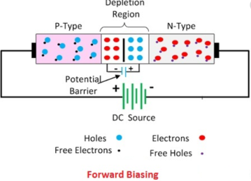
A P-N junction diode is said to be forward biased when the positive terminal of a cell or battery is connected to the p-side of the junction and the negative terminal to the n side.
When diode is forward-biased the depletion region narrows and consequently, the potential barrier is lowered. This causes the majority charge carriers of each region to cross into the other region.
The electrons travel from the n-side to the p-side and go to the positive terminal of the battery. The holes that travel from the p-side to the n-side combine with the electrons injected into the n-region from the negative terminal of the battery.
This way the diode conducts when forward-biased.
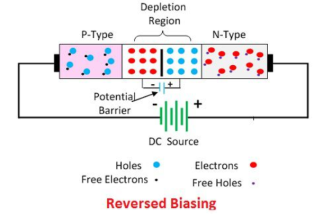
Reverse-biased
A pn-junction diode is said to be reverse biased when the positive terminal of a cell or battery is connected to the n-side of the junction and the negative terminal to the p-side.
When reverse biased, the depletion region widens and the potential barrier is increased. The polarity of the battery extracts the majority charge carriers of each region.
The holes in the p-region from the electrons injected into the p-region from the negative terminal of the battery. The electrons in the n-region go to the positive terminal of the battery.
This way, the majority charge carrier concentration in each region decreases against the equilibrium values and the reverse biased junction diode has a high resistance. Thus, the diffusion current across the junction becomes zero.
Thus, the diode does not conduct when reverse biased and is said to be in a quiescent or non-conducting state i.e., it acts as an open switch.
- Zener diode,
- A Zener diode is a silicon semiconductor device that permits current to flow in either a forward or reverse direction.
- The diode consists of a special, heavily doped p-n junction, designed to conduct in the reverse direction when a certain specified voltage is reached.
- The Zener diode has a well-defined reverse-breakdown voltage, at which it starts conducting current, and continues operating continuously in the reverse-bias mode without getting damaged.
- Additionally, the voltage drop across the diode remains constant over a wide range of voltages, a feature that makes Zener diodes suitable for use in voltage regulation.
Operation
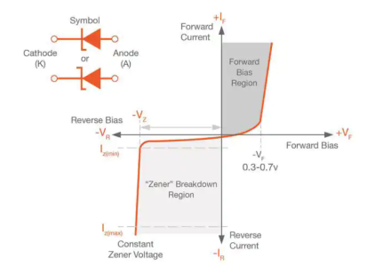
The Zener diode operates just like the normal diode when in the forward-bias mode, and has a turn-on voltage of between 0.3 and 0.7 V.
However, when connected in the reverse mode, which is usual in most of its applications, a small leakage current may flow.
As the reverse voltage increases to the predetermined breakdown voltage (Vz), a current start flowing through the diode.
The current increases to a maximum, which is determined by the series resistor, after which it stabilizes and remains constant over a wide range of applied voltage.
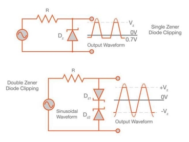
Figure : Zener diode IV characteristics
Zener breakdown
The breakdown is either due to the Zener breakdown effect that occurs below 5.5 V, or impact ionization that occurs above 5.5 V.
Both mechanisms result in the same behaviour and do not require different circuitry; however, each mechanism has a different temperature coefficient.
The Zener effect has a negative temperature coefficient while the impact effect experiences a positive coefficient.
The two temperature effects are almost equal at 5.5 V and cancel out each other to make the Zener diodes rated at around 5.5 V the most stable over a wide range of temperature conditions.
- Rectifiers: Half wave, full wave – bridge and centre tap, L and C filters for smoothing
A complete half-wave rectifier circuit consists of 3 main parts:
- A transformer
- A resistive load
- A diode
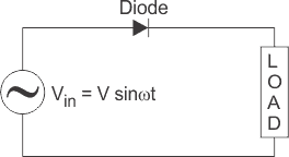
A half wave rectifier circuit diagram looks like this:
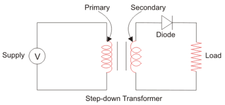
First, a high AC voltage is applied to the to the primary side of the step- down transformer and we will get a low voltage at the secondary winding which will be applied to the diode.

During the positive half cycle of the AC voltage, the diode will be forward biased and the current flows through the diode. During the negative half cycle of the AC voltage, the diode will be reverse biased and the flow of current will be blocked. The final output voltage waveform on the secondary side (DC) is shown in figure above.
If we replace the secondary transformer coils with a source voltage, we can simplify the circuit diagram of the half-wave rectifier as:
For the positive half cycle of the AC source voltage, the equivalent circuit effectively becomes:
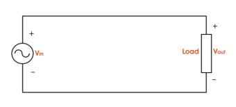
This is because the diode is forward biased, and is hence allowing current to pass through. So, we have a closed circuit.
But for the negative half cycle of the AC source voltage, the equivalent circuit becomes:
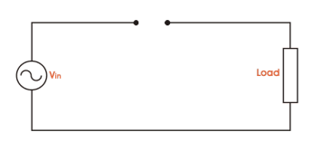
Because the diode is now in reverse bias mode, no current is able to pass through it. As such, we now have an open circuit. Since current cannot flow through to the load during this time, the output voltage is equal to zero.
This all happens very quickly – since an AC waveform will oscillate between positive and negative many times each second (depending on the frequency).
Here’s what the half wave rectifier waveform looks like on the input side (Vin), and what it looks like on the output side (Vout) after rectification (i.e. conversion from AC to DC):
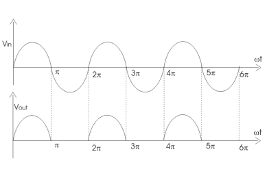
The graph above actually shows a positive half wave rectifier. This is a half-wave rectifier which only allows the positive half-cycles through the diode,and blocks the negative half-cycle.
The voltage waveform before and after a positive half wave rectifier is shown in figure 4 below.

Conversely, a negative half-wave rectifier will only allow negative half-cycles through the diode and will block the positive half-cycle. The only difference between a posive and negative half wave rectifier is the direction of the diode.
As you can see in figure 5 below, the diode is now in the opposite direction. Hence the diode will now be forward biased only when the AC waveform is in its negative half cycle.

ADVANTAGES:-
1)Simple Construction.
2) Component required less.
3)Small size.
APPLICATION:-
Walkman, low-cost power supply.
TRANSFORMER UTILISATION FACTOR(TUF): It indicates how well the ilp transformer is being utilized
TUF= DC O/P Power / AC power rating of the transformer

Full wave rectifier
1) A center-tapped rectifier is a type of full-wave rectifier that uses two diodes connected to the secondary of a center-tapped transformer.
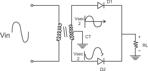
Center tapped full wave rectifier operation:-
I) During the positive half cycle of the i/p ac supply.
Diagram

D1.Is in forward biased & D2 is in reverse biased.
II)During -ve half cycle.

D1 Reverse biased
D2 Forward biased
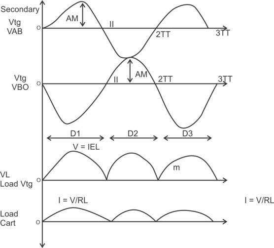
ADVANTAGES
- Law ripple factor as Compared to HKR.
- Better rectification efficiency.
- Better TUF.
- A higher value of average load vtg & avg load crt.
- No possibility of transformer core saturation.
DISADVANTAGES
PIV of the diode is 2vm, more size costly.
APPLICATION
I) Battery charges.
2)power supply at the laboratory, high current, electronic ckt.
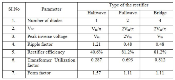
L and C filter for smoothing:
The name pi – Filter implies to the resemblance of the circuit to a Π shape with two shunt capacitances (C1 and C2) and an inductance filter ‘L’. As the rectifier output is provided directly into the capacitor it also called a capacitor input filter.
The output from the rectifier is first given to the shunt capacitor C. The rectifier used can be half or full wave and the capacitors are usually electrolytic even though they large in size. In practical applications, the two capacitances are enclosed in a metal container which acts as a common ground for the two capacitors. Circuit diagram and the waveform are given below.

When compared to other type of filters, the Π – Filter has some advantages like higher dc voltage and smaller ripple factor. But it also has some disadvantages like poor voltage regulation, high peak diode current, and high peak inverse voltage.
This filter is divided into two – a capacitor filter and a L-section filter. The capacitor C1 does most of the filtering in the circuit and the remaining ripple os removed by the L-section filter (L-C2). C1 is selected to provide very low reactance to the ripple frequency. The voltage regulation is poor for this circuit as the output voltage falls off rapidly with the increase in load current.
Bipolar junction transistor
A Bipolar Junction Transistor (also known as a BJT or BJT Transistor) is a three-terminal semiconductor device consisting of two p-n junctions which to amplify or magnify a signal.
It is a current controlled device. The three terminals of the BJT are the base, the collector, and the emitter. A BJT is a type of transistor that uses both electrons and holes as charge carriers.
There are two types of bipolar junction transistors –NPN and PNP transistors. A diagram of these two types of bipolar junction transistors is given below.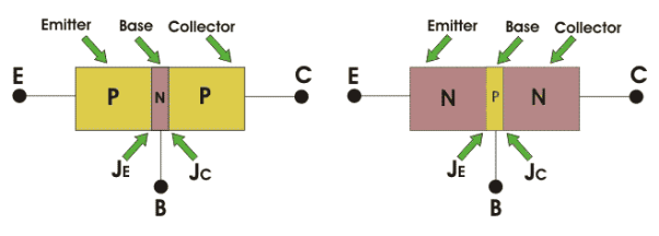
From the above figure, we can see that every BJT has three parts named emitter, base and collector. JE and JC represent the junction of emitter and junction of collector respectively. Now initially it is sufficient for us to know that emitter- based junction is forward biased and collector-base junctions are reverse biased.
Construction and biasing
In an n-p-n bipolar transistor one p-type semiconductor resides between two n-type semiconductors the diagram below an n-p-n transistor is shown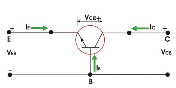
Now IE, IC is emitter current and collect current respectively and VEB and VCB are emitter-base voltage and collector-base voltage respectively.
According to the convention if for the emitter, base and collector current IE, IB and IC current goes into the transistor the sign of the current is taken as positive and if current goes out from the transistor then the sign is taken as negative.
For p-n-p bipolar junction transistor , n-type semiconductor is sandwiched between two p-type semiconductors. The diagram of a p-n-p transistor is shown below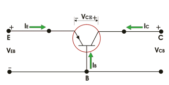
For p-n-p transistors, current enters into the transistor through the emitter terminal. Like any bipolar junction transistor, the emitter-base junction is forward biased, and the collector-base junction is reverse biased.
Biasing
Transistors are one of the largely used semiconductor devices which are used for wide variety of applications including amplification and switching. However to achieve these functions satisfactorily, transistor has to be supplied with certain amount of current and/or voltage. The process of setting these conditions for a transistor circuit is referred to as Transistor Biasing.
Some of the biasing circuits are:
Fixed Base Bias or Fixed Resistance Bias
The biasing circuit shown by Figure has a base resistor RB connected between the base and the VCC. Here the base-emitter junction of the transistor is forward biased by the voltage drop across RB which is the result of IB flowing through it.
From the figure, the mathematical expression for IB is obtained as
IB = Vcc – VBE / RB
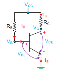
Here the values of VCC and VBE are fixed while the value for RB is constant once the circuit is designed.
This leads to a constant value for IB resulting in a fixed operating point due to which the circuit is named as fixed base bias.
This kind of bias, results in a stability factor of (β+1) which leads to very poor thermal stability.
VB = VBE = VCC – IBRB
Vc= Vcc – Ic Rc = VCC – VCE
Ic = β IB
IE ͌ IC
Collector Feedback Bias
In this circuit (Figure 2), the base resistor RB is connected across the collector and the base terminals of the transistor. This means that the base voltage, VB and the collector voltage, VC are inter-dependent due to the fact that
VB = VC – IB RB
Vc = Vcc – (IB + IC) RC
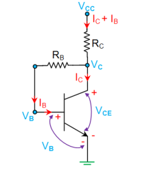
From these equations, it is seen that an increase in IC decreases VC which results in a reduced IB, automatically reducing IC.
This indicates that, for this type of biasing network, the Q-point (operating point) remains fixed irrespective of the variations in the load current causing the transistor to always be in its active region regardless of β value.
Here, other voltages and currents are expressed as
VB = VBE
IC = β IB
IE ͌ IC
Voltage Divider Bias
This type of biasing network (Figure7) employs a voltage divider formed by the resistors R1 and R2 to bias the transistor.
This means that here the voltage developed across R2 will be the base voltage of the transistor which forward biases its base-emitter junction.
In general, the current through R2 will be fixed to be 10 times required base current, IB (i.e. I2 = 10IB).
This is done to avoid its effect on the voltage divider current or on the changes in β. Further, from the circuit, one gets
IB = Vcc . R2/ R1 + R2
VE = IE RE
VB = I2 R2 = VBE + VE
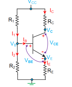
In this kind of biasing, IC is resistant to the changes in both β as well as VBE which results in a stability factor of 1 (theoretically), the maximum possible thermal stability. This is because, as IC increases due to a rise in temperature, IE also increases causing an increase in the emitter voltage VE which in turn reduces the base-emitter voltage, VBE. This results in the decrease of base current IB which restores IC to its original value. The higher stability offered by this biasing circuit makes it to be most widely used inspite of providing a decreased amplifier gain due to the presence of RE.
Configuration, transistor as a switch and amplifier
The three types of configurations are Common Base, Common Emitter and Common Collector configurations. In every configuration, the emitter junction is forward biased and the collector junction is reverse biased.
Common Base CB
The name itself implies that the Base terminal is taken as common terminal for both input and output of the transistor. The common base connection for both NPN and PNP transistors is as shown in the following figure.
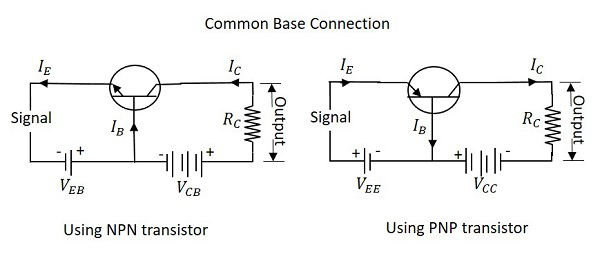
For the sake of understanding, let us consider NPN transistor in CB configuration. When the emitter voltage is applied, as it is forward biased, the electrons from the negative terminal repel the emitter electrons and current flows through the emitter and base to the collector to contribute collector current. The collector voltage VCB is kept constant throughout this.
In the CB configuration, the input current is the emitter current IE and the output current is the collector current IC.
Current Amplification Factor α
The ratio of change in collector current ΔIC to the change in emitter current ΔIE when collector voltage VCB is kept constant, is called as Current amplification factor. It is denoted by α.
α=ΔIC/ΔIE at constant VCB
Expression for Collector current
Along with the emitter current flowing, there is some amount of base current IB which flows through the base terminal due to electron hole recombination. As collector-base junction is reverse biased, there is another current which is flown due to minority charge carriers. This is the leakage current which can be understood as Ileakage. This is due to minority charge carriers and hence very small.
The emitter current that reaches the collector terminal is
αIE
Total collector current
IC=αIE +I leakage
If the emitter-base voltage VEB = 0, even then, there flows a small leakage current, which can be termed as ICBO collector−basecurrentwithoutputopencollector−basecurrentwithoutputopen.
The collector current therefore can be expressed as
IC=αIE+ICBO
IE=IC+IB
IC=α(IC+IB)+ICBO
IC(1−α)=αIB+ICBO
IC=(α1−α)IB+(ICBO1−α)
IC=(α1−α)IB+(11−α)ICBO
Hence the above derived is the expression for collector current. The value of collector current depends on base current and leakage current along with the current amplification factor of that transistor in use.
Characteristics of CB configuration
- This configuration provides voltage gain but no current gain.
- Being VCB constant, with a small increase in the Emitter-base voltage VEB, Emitter current IE gets increased.
- Emitter Current IE is independent of Collector voltage VCB.
- Collector Voltage VCB can affect the collector current IC only at low voltages, when VEB is kept constant.
- The input resistance ri is the ratio of change in emitter-base voltage ΔVEB to the change in emitter current ΔIE$ at constant collector base voltage VCB.
η=ΔVEB/ΔIE at constant VCB
- As the input resistance is of very low value, a small value of VEB is enough to produce a large current flow of emitter current IE.
- The output resistance ro is the ratio of change in the collector base voltage $ΔVCB$$ΔVCB$ to the change in collector current ΔIC at constant emitter current IE.
Ro=ΔVCB/ΔIC at constant lE
- As the output resistance is of very high value, a large change in VCB produces a very little change in collector current IC.
- This Configuration provides good stability against increase in temperature.
- The CB configuration is used for high frequency applications.
Common Emitter CE
The name itself implies that the Emitter terminal is taken as common terminal for both input and output of the transistor. The common emitter connection for both NPN and PNP transistors is as shown in the following figure.
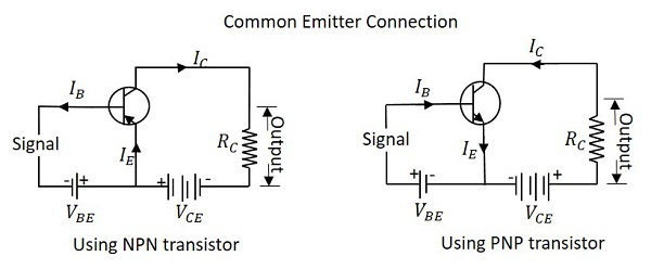
Just as in CB configuration, the emitter junction is forward biased and the collector junction is reverse biased. The flow of electrons is controlled in the same manner. The input current is the base current IB and the output current is the collector current IC here.
Base Current Amplification factor β
The ratio of change in collector current ΔIC to the change in base current ΔIB is known as Base Current Amplification Factor. It is denoted by β
β=ΔICΔ/IB
Relation between β and α
Let us try to derive the relation between base current amplification factor and emitter current amplification factor.
β=ΔIC/ΔIB
α=ΔIC/ΔIE
IE=IB+IC
ΔIE=ΔIB+ΔIC
ΔIB=ΔIE−ΔIC
We can write
β=ΔIC/ΔIE−ΔIC
Dividing by ΔIE
β=ΔIC/ΔIE/ΔIE/ΔIE−ΔIC/ΔIE
We have
α=ΔIC/ΔIE
Therefore,
β=α/1−α
From the above equation, it is evident that, as α approaches 1, β reaches infinity.
Hence, the current gain in Common Emitter connection is very high. This is the reason this circuit connection is mostly used in all transistor applications.
Expression for Collector Current
In the Common Emitter configuration, IB is the input current and IC is the output current.
We know
IE=IB+IC
And
IC=αIE+ICBO
=α(IB+IC)+ICBO
IC(1−α)=αIB+ICBO
IC=α/1−α IB+1/1−α ICBO
If base circuit is open, i.e. if IB = 0,
The collector emitter current with base open is ICEO
ICEO=1/1−αICBO
Substituting the value of this in the previous equation, we get
IC=α/1−α . IB+ ICEO
IC=βIB+ICEO
Hence the equation for collector current is obtained.
Knee Voltage
In CE configuration, by keeping the base current IB constant, if VCE is varied, IC increases nearly to 1v of VCE and stays constant thereafter. This value of VCE up to which collector current IC changes with VCE is called the Knee Voltage. The transistors while operating in CE configuration, they are operated above this knee voltage.
Characteristics of CE Configuration
- This configuration provides good current gain and voltage gain.
- Keeping VCE constant, with a small increase in VBE the base current IB increases rapidly than in CB configurations.
- For any value of VCE above knee voltage, IC is approximately equal to βIB.
- The input resistance ri is the ratio of change in base emitter voltage ΔVBE to the change in base current ΔIB at constant collector emitter voltage VCE.
Ri=ΔVBE/ΔIB at constant VCE
- As the input resistance is of very low value, a small value of VBE is enough to produce a large current flow of base current IB.
- The output resistance ro is the ratio of change in collector emitter voltage ΔVCE to the change in collector current ΔIC at constant IB.
Ro=ΔVCE/ΔIC at constant IB
- As the output resistance of CE circuit is less than that of CB circuit.
- This configuration is usually used for bias stabilization methods and audio frequency applications.
Common Collector CC Configuration
The name itself implies that the Collector terminal is taken as common terminal for both input and output of the transistor. The common collector connection for both NPN and PNP transistors is as shown in the following figure.
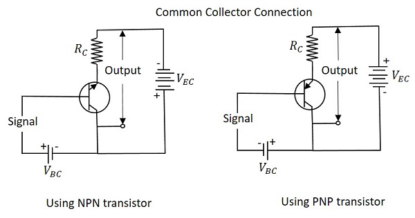
Just as in CB and CE configurations, the emitter junction is forward biased and the collector junction is reverse biased. The flow of electrons is controlled in the same manner. The input current is the base current IB and the output current is the emitter current IE here.
Current Amplification Factor γ
The ratio of change in emitter current ΔIE to the change in base current ΔIB is known as Current Amplification factor in common collector CC configuration. It is denoted by γ.
γ=ΔIE/ΔIB
- The current gain in CC configuration is same as in CE configuration.
- The voltage gain in CC configuration is always less than 1.
Relation between γ and α
Let us try to draw some relation between γ and α
γ=ΔIE/ΔIB
α=ΔIC/ΔIE
IE=IB+IC
ΔIE=ΔIB+ΔIC
ΔIB=ΔIE−ΔIC
Substituting the value of IB, we get
γ=ΔIE/ΔIE−ΔIC
Dividing by ΔIEΔIE
γ=ΔIE/ΔIE/ΔIE/ΔIE−ΔIC/ΔIE
1/1−α1
γ=1/1−α
Expression for collector current
We know
IC=αIE+ICBOIC=αIE+ICBO
IE=IB+IC=IB+(αIE+ICBO)IE=IB+IC=IB+(αIE+ICBO)
IE(1−α)=IB+ICBOIE(1−α)=IB+ICBO
IE=IB1−α+ICBO1−αIE=IB1−α+ICBO1−α
IC≅IE=(β+1)IB+(β+1)ICBO
The above is the expression for collector current.
Characteristics of CC Configuration
- This configuration provides current gain but no voltage gain.
- In CC configuration, the input resistance is high and the output resistance is low.
- The voltage gain provided by this circuit is less than 1.
- The sum of collector current and base current equals emitter current.
- The input and output signals are in phase.
- This configuration works as non-inverting amplifier output.
- This circuit is mostly used for impedance matching. That means, to drive a low impedance load from a high impedance source.
Determine the levels of ICQ and VCEQ for voltage divider configuration using exact and approximate techniques and compare solutions.
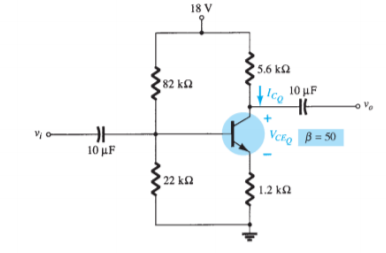
β . RE ≥ 10 R2
(50)(1.2 k Ω) ≥ 10(22 k Ω)
 60kΩ ≥ 220kΩ
Rth = R1 || R2 82 kΩ || 22 kΩ = 17.35 kΩ
Eth = R2 Vcc/ R1 + R2 = 22kΩ (18V)/ 82kΩ + 22kΩ = 3.81 V
IB = Eth – VBE/ Rth + (β +1) RE = 3.81 V – 0.7V / 17.35 kΩ + (51 )(1.2kΩ) = 3.11/ 78.55 kΩ = 39.6 μ A
ICQ = β IB = (50)(39.6μA) = 1.98 mA
VCEQ = Vcc – IC(RC + RE)
= 18V – (1.98mA)(5.6kΩ + 1.2 kΩ)= 4.54V
BJT as a switch
Suppose we had a lamp that we wanted to turn on and off with a switch. Such a circuit would be extremely simple, as in the figure below.

a- mechanical switch
b- NPN transistor switch
c- PNP transistor switch
Transistor as switch
Suppose we insert a transistor in place of the switch to show how it can control the flow of electrons through the lamp. Remember that the controlled current through a transistor must go between collector and emitter.

Transistor: a) cut-off lamp b) saturated, lamp on.
The choice between NPN and PNP is really arbitrary. All that matters is that the proper current directions are maintained for the sake of correct junction biasing.
In the above figures, the base of either BJT is not connected to a suitable voltage, and no current is flowing through the base. Consequently, the transistor cannot turn on. Therefore, connect a switch between the base and collector wires of the transistor as in figure.
If the switch is open as in figure (a), the base wire of the transistor will be left “floating” and there will be no current through it. In this state, the transistor is said to be cut-off.
If the switch is closed as in figure (b), current will be able to flow from the base to the emitter of the transistor through the switch. This base current will enable a much larger current flow from the collector to the emitter, thus lighting up the lamp. In this state of maximum circuit current, the transistor is said to be saturated.
BJT as an Amplifier
Transistor raises the strength of a weak signal and hence acts an amplifier. The transistor amplifier circuit is shown in the figure below.
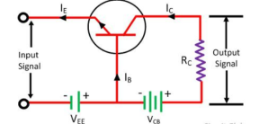
Transistor as an Amplifier
The transistor has three terminals namely emitter, base and collector. The emitter and base of the transistor are connected in forward biased and the collector base region is in reverse bias. The forward bias means the P-region of the transistor is connected to the positive terminal of the supply and the negative region is connected to the N-terminal and in reverse bias just opposite of it has occurred.
Vee is applied to the input circuit along with the input signal to achieve the amplification. The DC voltage VEE keeps the emitter-base junction under the forward biased condition regardless of the polarity of the input signal and is known as bias voltage.
When a weak signal is applied to the input, a small change in signal voltage causes a change in emitter current this change is almost the same in collector current because of the transmitter action.
In the collector circuit, a load resistor RC of high value is connected. When collector current flows through such a high resistance, it produces a large voltage drop across it. Thus, a weak signal (0.1V) applied to the input circuit appears in the amplified form (10V) in the collector circuit.
Input Resistance
When the input circuit is forward biased, the input resistance will be low. The input resistance is the opposition offered by the base-emitter junction to the signal flow.
Hence, it is the ratio of small change in base-emitter voltage (ΔVBE) to the resulting change in base current (ΔIB) at constant collector-emitter voltage.
Input resistance, Ri=ΔVBE/ΔIb
Where Ri = input resistance, VBE = base-emitter voltage, and IB = base current.
Output Resistance
The output resistance of a transistor amplifier is very high. The collector current changes very slightly with the change in collector-emitter voltage.
The ratio of change in collector-emitter voltage (ΔVCE) to the resulting change in collector current (ΔIC) at constant base current.
Output resistance = Ro=ΔVCE/ΔIC
Where Ro = Output resistance, VCE = Collector-emitter voltage, and IC = Collector-emitter voltage.
Current gain
It is the ratio of change in collector current (ΔIC) to the change in base current (ΔIB).
Current gain, β=ΔIC/ ΔIB
Voltage Gain
It is the ratio of change in output voltage (ΔVCE) to the change in input voltage (ΔVBE).
Voltage gain, AV=ΔVCE/ΔVBE
= ΔIC x RAC / ΔIB x Ri = ΔIC / ΔIB x RAC / Ri = β x R AC/ Ri
Power Gain
It is the ratio of output signal power to the input signal power.
Power gain Ap = (ΔIC) 2 x RAC / (ΔIB ) 2 x Ri
= (ΔIC / ΔIB) x ΔIC x RAC / ΔIB x Ri
= current gain x voltage gain
References:
- Electronic Devices And Circuits Theory 10th Edition (English, Paperback, Robert L. Boylestad, Louis Nashelsky)
Electronic Principles Textbook by Albert Paul Malvino
How to Diagnose and Fix Everything Electronic, Second Edition Book by Michael Jay Geier
- Principles of Electronics is a 2002 book by Colin Simpson
Starting Electronics Book by Keith Brindley