UNIT 6
NANOSCIENCE
Introduction
In recent years nanotechnology has become one of the most important and exiting forefront fields in physics, chemistry, biology and engineering and technology. Nano means 10-9 m. A nanometer (nm) is one thousand millionth of a meter. Atoms are extremely small and the diameter of a single atom varies from 0.1 to 0.5 nm depending on the type of the element. For example, one carbon atom is approximately 0.15nm in diameter and a water molecule is almost 0.3nm across. A red blood cell is approximately 7,000 nm wide and human hair is 80,000 nm wide.
Origin of Nano technology
While the word Nano technology is relatively new, the existence of nanostructures and Nano devices is not new. Such structures existed on the earth as life itself began though it is not known when humans to use nanosized materials the first known, Roman glassmakers were fabricated glasses containing nanosized metals. When the material size of the object is reduced to nanoscale, then it exhibits different properties than the same material in bulk form.
The concept and idea of nanotechnology original discussed first time in 1959 by Richard Feynman, the renowned physicist. Richard Feynman in his talk “There's Plenty of Room at the Bottom,” described the feasibility of synthesis via direct manipulation of atoms. However, in 1974, the term "Nano-technology" was first used by Norio Taniguchi.
Nanoscience
Nano science deals with the study of properties of materials at nano scales where properties differ significantly than those at larger scale.
Nanotechnology
Nanotechnology deals with the design, characterization, production and applications of nanostructures and nanodevices and nanosystems.
Properties of nanomaterials
Physical properties
Inter atomic distance: When the material size is reduced to Nano scale, surface area to volume ratio increases. Due to increase of surface of surface area, more number of atoms will appear at the surface of compared to those inside. So Interatomic spacing decreases with size.
Thermal properties: Nano materials are different from that of bulk materials. The Debye Temperature and ferroelectric phase transition temperature are lower for nano materials. The melting point of nano gold decreases from 1200 K to 800K as the size of particle decreases form 300 Å to 200 Å.
Optical properties: Different sized nano particles scatters different of light incident on it and hence they appear with different colours. For example nano gold does not act as bulk gold. The nano particles of gold appear as orange, purple, red or greenish in colour depending on their grain size. The bulk copper is opaque whereas nanoparticle copper is transparent.
Magnetic properties: The magnetic properties of nano materials are different from that of bulk materials. In explaining the magnetic behaviour of nanomaterials, we use single domains unlike large number of domains in bulk materials. The coercivity value of single domain is very large.
For example, Fe, Co, and Ni are ferromagnetic in bulk but they exhibit super par magnetism. Na, K, and Rh are paramagnetic in bulk but they exhibit ferro-magnetic. Cr is anti-ferromagnetic in bulk but they exhibit super paramagnetic.
Mechanical properties: The mechanical properties such as hardness, toughness, elastic modulus, young’s modulus etc., of nano materials are different from that of bulk materials. In metals and alloys, the hardness and toughness are increased by reducing the size of the nano particles. In ceramics, ductility and super plasticity are increased on reducing grain size. Hardness increases 4 to 6 times as one goes from bulk Cu to nanocrystalline and it is 7 to 8 times for Ni.
Chemical properties
Nanocrystalline materials are strong, hard, erosion and corrosion resistant. They are chemically active and have the following chemical properties.
- In electrochemical reactions, the rate of increase in mass transport increases as the particle size decreases.
- The equilibrium vapour pressure, chemical potentials and solubilites of nanoparticles are greater than that for the same bulk material.
- Most of the metals do not absorb hydrogen. But the hydrogen absorption increases with the decrease of cluster size in Ni, Pt and Pd metals.
Basic principles of nanomaterials
When the material size of the object is reduced to nanoscale, then it exhibits different properties than the same material in bulk form. The factors that differentiates the nanomaterials from bulk material is
- Increase in surface area to volume ratio
- Quantum confinement effect
Increase in surface area to volume ratio: The ratio of surface area to volume ratio is large for nano materials.
Example 1: To understand this let us consider a spherical material of radius ‘r’. Then its surface area to volume ratio is 3/r. Due to decrease of r, the ratio increases predominantly.
Example 2: For one cubic volume, the surface ratio is 6m2. When it is divided into eight cubes its surface area becomes 12m2. When it is divided into 27 cubes its surface area becomes 18m2. Thus, when the given volume is divided into smaller pieces the surface area increases.

Due to increase of surface of surface area, more number of atoms will appear at the surface of compared to those inside. For example, a nano material of size 10nm has 20% of its atoms on its surface and 3nm has 50% of its atoms. This makes the nanomaterials more chemically reactive and affects the properties of nano materials.
Quantum confinement effect: According to band theory, the solid atoms have energy bands and isolated atoms possess discrete energy levels. Nano materials are the intermediate state to solids and atoms. When the material size is reduced to nanoscale, the energy levels of electrons change. This effect is called quantum confinement effect. This affects the optical, electrical and magnetic properties of nanomaterials.
Nano materials
All materials are composed of grains. The visibility of grains depends on their size. Convectional materials have grains varying in size from hundreds of microns to millimetres. The materials processing grains size ranging from 1 to 100 nm, known as Nano materials. Nano materials can be produced in different dimensionalities.
- One dimensional nano material: Surface coatings and thin films
- Two dimensional nano materials: nano tubes nano wires, biopolymers
- Three dimensional nano materials: nano particles, precipitates, colloids, quantum dots, nano crystalline materials, fullerenes or carbon nano-60.
Classification of nanostructured materials
In the past two decades, hundreds of novel NSMs (nanostructured materials) have been obtained therefore, the need in their classification become important.
NSMs as a subject of nanotechnology are low dimensional materials comprising of building units of a submicron or nanoscale size at least in one direction and exhibiting size effects.
The first classification idea of NSMs was given by Gleiter in 1995 and further was explained by Skorokhod in 2000. However, Gleiter and Skorokhod scheme was not fully considered because of 0D, 1D, 2D, and 3D structures such as fullerenes, nanotubes, and nanoflowers were not taken into account.
After them Pokropivny and Skorokhod reported a modified classification scheme for NSMs, in which 0D, 1D, 2D and 3D NSMs are included.
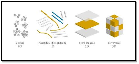
- 0D Nanostructured Materials
In the past 10 years, significant progress has been made in the field of 0D NSMs. 0D NSMs such as uniform particles arrays (quantum dots), heterogeneous particles arrays, core–shell quantum dots, onions, hollow spheres and nanolenses have been synthesized by several research groups. 0D NSMs, such as quantum dots has been extensively studied in light emitting diodes (LEDs), solar cells, single-electron transistors, and lasers.
A 0D structure is the simplest block that can be used for the design of nanomaterials. In this case, the three dimensions are in the nanometre regime and have a diameter less than 100 nm. Nanoparticles, nanocrystals, and nanoclusters correspond to this group.
Nanoparticles
They are nanostructures usually used to define all 0D nanostructures or those that are amorphous and have an irregular shape. So, the nanoparticles can be of natural origin, semiconductor, metal, oxides, fullerenes or quantum dots.
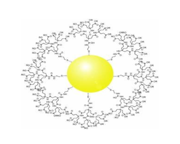
Figure: Nanoparticle
During manufacturing, the nanoparticles that make up the nanomaterials can be of different sizes, which can vary by more than 15% and still form the nanomaterial without affecting its design. 3D nanomaterials should not be included in the category of nanostructures unless their internal structure is nanostructured.
Nanoclusters
As well as the nanoparticles, they have an irregular structure besides being semi crystalline, but they are tinier than the nanoparticles. Its diameter ranges between 1 and 10 nm.
Also nanoclusters are sensitive to their size and become more reactive if they increase or decrease proportionally.
Nanocrystals
They are monocrystalline nanostructures, whose size ranges from 1 to 30 nm. Semiconductor nanocrystals are more commonly known as quantum dots.
- One-dimensional nanomaterials (1D)
In the last decade, 1D NSMs have stimulated an increasing interest due to their importance in research and developments and have a wide range of potential applications. It is generally accepted that 1D NSMs are ideal systems for exploring a large number of novel phenomena at the nanoscale and investigating the size and dimensionality dependence of functional properties.
They are also expected to play an important role as both interconnects and the key units in fabricating electronic, optoelectronic, and EEDs with nanoscale dimensions. The field of 1D NSMs such as nanotubes has attained a significant attention. 1D NSMs have a profound impact in nanoelectronics, nanodevices and systems, nanocomposite materials, alternative energy resources and national security. We show the 1D NSMs, such as nanowires, nanorods, nanotubes, nanobelts, nanoribbons, and hierarchical nanostructures, which have been synthesized in the laboratories. They have a variable length, conserving two dimensions (height and width) in the nanometer regime; to these correspond the nanowires and nanotubes.
Nanowires
They are elongated crystalline structures whose characteristics stand out for their conductive or semiconducting properties. Nanowires have been obtained from various metallic materials, semiconductors, oxides, etc. In recent years, nanowires have shown special scientific interest due to their potential applications in nanoelectronics, optoelectronics, and sensors.
Nanotubes
They are tubular structures with a hollow interior. There are nanotubes synthesized and characterized from inorganic laminar materials. However, the most studied are carbon nanotubes (CNT's).
Carbon nanotubes: Carbon nanotubes were first observed b Sunmino Iijima in 1911. Carbon exists in a large number of allotropic forms. These includes diamond, graphite and fullerenes (such as C60 , C70 etc.,). Carbon nanotubes are obtained by rolling the graphite sheet into tubes with the bonds at the ends of the sheet. These bonds are used to close the tube. Generally, the length of carbon nanotubes varies from several micrometres to millimetre and the diameter will vary from 1 to 20 nm.
A tube may contain one cylindrical wall of graphite or a number of concentric cylindrical walls. A carbon nanotube consisting of one cylindrical graphite is called single walled nanotube. Otherwise they are known as multi walled nanotubes.
Depending on how sheet is rolled, they are classified into three types. The three types of carbon nanotubes are 1) Zigzag 2) Chiral 3) Armchair
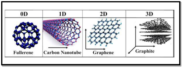
Properties of carbon nanotubes
Electrical conductivity: Generally the carbon nanotubes produced both in metallic and semiconducting in their electrical behaviour. Conductivity of multi walled nanotube id more complex. The conductivity and resistivity of ropes of single walled carbon nanotubes has been measured by placing the electrodes at different parts of the carbon nanotubes. The resistivity of single walled carbon nanotube ropes was of the order of 10-4 ohm-cm at 270. This means that the conductivity of single walled nanotube ropes are most conductive carbon fibres of known.
Magnetic property: The carbon nanotube displays the magneto-resistive effects at lower temperature i.e., the resistance of the carbon nanotube is changed by the application of dc magnetic field. The variation of resistance in carbon nanotube at 2.3K and 0.36k w.r.t magnetic field is observed. This show magneto- resistance effect is negative. This is due to the decrease in resistance with increase in magnetic field.
Highly absorbent: The carbon nanotubes have large surface area and high absorbance. So the carbon nanotubes are used in the air, gas and water filtration.
Mechanical properties: The strength of the sp2 carbon-carbon bonds gives carbon nanotubes amazing mechanical properties. The stiffness of the material is measured in terms of its Young’s modulus. The Young’s modulus value of single walled nanotube is about 1Tera Pascal, which is approximately 5 times greater than steel. The tensile strength or breaking strain of nanotube is about 150GPa, which is approximately 150 times greater than steel
Vibration properties: Similar to carbon dioxide molecule, Carbon nanotubes have two normal modes of vibration (a set of vibrational motions known as normal mode of vibrations). The different modes of vibrational motion are determined from the symmetry of the molecule. In the first mode the diameter of the carbon nanotube moves in and out at the frequency of 165 cm-1. In the second mode the carbon nanotube crushing in one direction and expansion takes place in the perpendicular direction. Thus, it oscillates between sphere and ellipse at a frequency of 17 cm-1. The frequency of the vibration modes depends on the diameter of the nanotube.
- Two-dimensional nanomaterials (2D)
2D nanostructures have two dimensions outside of the nanometric size range. In recent years, a synthesis 2D NSMs have become a focal area in materials research, owing to their many low dimensional characteristics different from the bulk properties. In the search of 2D NSMs, considerable re-search attention has been focused over the past few years on the development of 2D NSMs. 2DNSMs with certain geometries exhibit unique shape-dependent characteristics and subsequent utilization as building blocks for the key components of nanodevices.
In addition, a 2D NSMs are particularly interesting not only for basic understanding of the mechanism of nanostructure growth, but also for investigation and developing novel applications in sensors, photo catalysts, nano-containers, nanoreactors, and templates for 2D structures of other materials.
There are 2D NSMs such as junctions (continuous islands), branched structures, nanoprisms, nanoplates, nanosheets, nanowalls, and nanodisks.
They are basically nanomaterials formed by very thin layers; thin nanolayers with areas of undefined size and a thickness between 1 and 100 nm.
Graphene is the most notable example because, due to its multiple and exceptional properties, it has the potential to revolutionize technology. Its possible applications extend to very diverse areas, ranging from the miniaturization of electronic devices to the elaboration of drugs against cancer in medicine.
The synthesis of nanomaterials is key to the future success of this new technology. The methods of producing nanoparticles are classified into two main categories: Bottom-up approach
Top-down approach
- Bottom up Approach
In bottom-up approaches nanomaterials are assembled from basic building blocks, such as molecules or nanoclusters. The basic building blocks, in general, are nanoscale objects with suitable properties that can be grown from elemental precursors. The concept of the bottom-up approach is that the complexity of nanoscale components should reside in their self-assembled internal structure, requiring as little intervention as possible in their fabrication from the macroscopic world.
The bottom-up approach uses atomic or molecular feed-stocks as the source of the material to be chemically transformed into larger nanoparticles. This has the advantage of being potentially much more convenient than the top down approach. By controlling the chemical reactions and the environment of the growing nanoparticle, then the size, shape and composition of the nanoparticles may all be affected. For this reason nanoparticles produced by bottom up, chemically based and designed, reactions are normally seen as being of higher quality and having greater potential applications. This has led to the growth of a host of common bottom up strategies for the synthesis of nanoparticles. Many of these techniques can be tailored to be performed in gas, liquid, solid states, hence the applicability of bottom-up strategies to a wide range of end products. Most of the bottom up strategies requires suitable organometallic complexes or metal salts to be used as chemical precursors, which are decomposed in a controlled manner resulting in particle nucleation and growth. One of the key differences that can be used to subdivide these strategies into different categories is the method by which the precursor is decomposed.
A typical example of bottom-up is processing for nanocomposite magnets from individual high-magnetization and high-coercivity nanoparticles. The assembling critically depends on availability of anisotropic (single crystal) hard magnetic nanoparticles. Anisotropic nanoparticles produced via surfactant-assisted high energy ball milling satisfy the major requirements for this application.
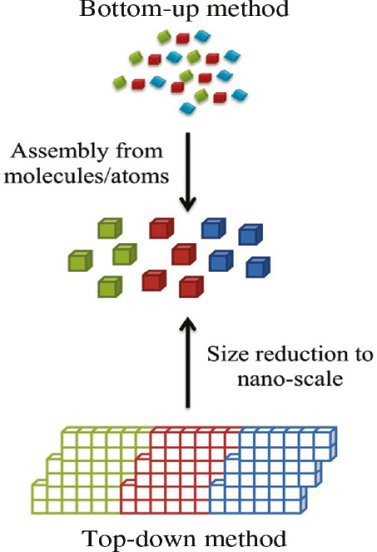
- Top down Approach
In top-down approaches, a bulk material is restructured (i.e. partially dismantled, machined, processed or deposited) to form nanomaterials. The aggressive scaling of electronic integrated circuits in recent years can be considered the greatest success of this paradigm. For top-down methods, the challenges increase as devices size is reduced and as the desired component designs become larger and more complex. Also the top-down assembly of nanocomponents over large areas is difficult and expensive.
The top-down method involves the systematic breakdown of a bulk material into smaller units using some form of grinding mechanism. This is beneficial and simple to execute and avoids the use of volatile and poisonous compounds frequently found in the bottom-up techniques. However, the quality of the nanoparticles formed by grinding is accepted to be poor in comparison with the material produced by modern bottom up methods. The main drawbacks include defect problems from grinding equipment, low particle surface areas, asymmetrical shape and size distributions and high energy needed to produce relatively small particles. Apart from these disadvantages, it must be distinguished that the nano-material produced from grinding still finds use, due to the simplicity of its manufacture, in applications including magnetic, catalytic and structural properties.
Nanomaterials behave differently as the size changes with respect to the bulk. It is necessary to characterize physical, structural and optical properties of a material to qualify as nanomaterial. Various characterization techniques are used to know the characteristics of the nanomaterials.
We will discuss the two techniques in this section.
- XRD Technique
- SEM (Scanning Electron Microscope) Technique
X-ray diffraction (XRD)
XRD is one of the most extensively used techniques for the characterization of nanoparticles. XRD provides information regarding the crystalline structure, nature of the phase, lattice parameters and crystalline grain size.
X-ray powder diffraction (XRD) is a rapid analytical technique primarily used for phase identification of a crystalline material and can provide information on unit cell dimensions. The analysed material is finely ground, homogenized, and average bulk composition is determined.
Powder X-ray diffraction has become a cornerstone technique for deriving crystallite size in nanoscience due to speed and "simplicity". An advantage of the XRD techniques commonly performed in samples of powder form, usually after drying their corresponding colloidal solutions, is that it results in statistically representative, volume-averaged values. The composition of the particles can be determined by comparing the position and intensity of the peaks. However, it is not suitable for amorphous materials and the XRD peaks are too broad for particles with a size below 3 nm.
Unfortunately, this apparently simple technique commonly has unexpected problems. Anisotropic peak broadening related to crystallite shape, defects, and microstrain occurs frequently in nanomaterials and can significantly complicate the analysis. In some instances, the usage of the conventional single peak approach would give erroneous results, and in others, this type of analysis is not even possible. A number of different nanocrystalline oxides have been examined to determine their crystallite sizes by different techniques. They differ in terms of crystal symmetry, crystallinity, density, and present different challenges with regard to size analysis.
Principle: X-ray diffraction is based on constructive interference of monochromatic X-rays and a crystalline sample. These X-rays are generated by a cathode ray tube, filtered to produce monochromatic radiation, collimated to concentrate, and directed toward the sample
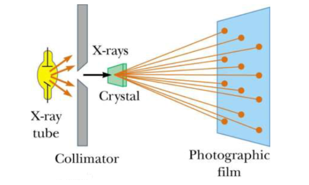
X-ray Diffraction (XRD) is one of the classical methods for identification and characterization of crystalline solids. Each crystalline solid has its unique characteristic X-ray powder pattern which issued as a ”fingerprint” for its identification. The method is based on the diffraction of X-rays by the sample in different directions. Waves of wavelength comparable to the crystal lattice spacing are strongly scattered (diffracted).
A powder X-ray diffractometer consists of an X-ray source (usually an X-ray tube), a sample stage, a detector and a way to vary angle θ. The X-ray is focused on the sample at some angle θ, while the detector opposite the source reads the intensity of the X-ray it receives at 2θ away from the source path. The incident angle is than increased over time while the detector angle always remains 2θ.
X-rays incident upon a crystal is scattered in different ways. When the wavelength of the radiation (λ) is comparable to the atomic spacing in a crystal, the scattering which is termed as diffraction, gives rise to a set of well-defined beams arranged with a characteristic geometry, thus forming a diffraction pattern. Schematic of X-ray diffraction setup is shown in figure.
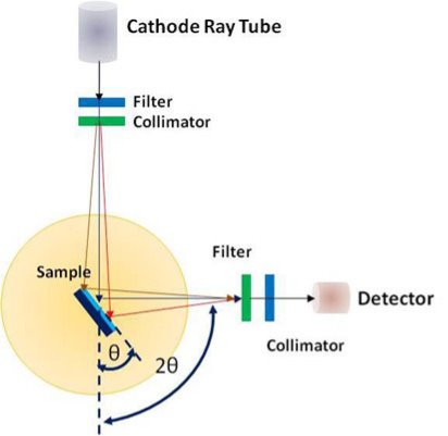
Figure: XRD Technique
X-ray diffraction data collection is the result of relative intensity (I) for each reflection with a set of planes in the crystal, designated by Miller indices (h k l), along with the corresponding scattering angle (2θ) for that reflection. The positions and intensities of the diffracted beams are a function of the arrangements of the atoms in space and some other atomic properties.
Thus, if the positions and the intensities of the diffracted beams are recorded, it is possible to deduce the arrangement of the atoms in the crystal and their chemical nature. A beam of radiation will only be diffracted when it imposed upon a set of planes in a crystal if the geometry of the situation fulfils quite specific law defined by Bragg’s known as Bragg’s law.
nλ =2dhkl sinθ
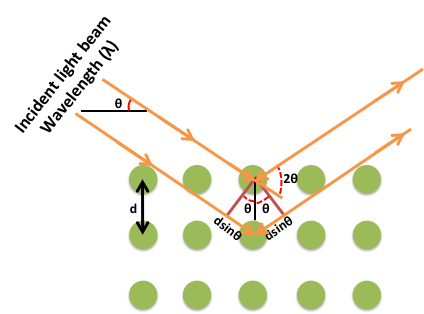
Figure: Bragg’s Law
The above equation is known as the Bragg equation, where n denotes the order of diffraction, λ represents the wavelength, d is the interplanar spacing of hkl planes in crystal lattice and θ signifies the Bragg angle.
A typical diffraction pattern shows the intensity Vs 2θ plot. Each peak corresponds to a specific (h k l) plane of the sample. The broadening of the diffraction peaks is due to two factors:
1) Due to size of crystallite
2) Due to micro strain of crystallite
Advantages
- It is a rapid and powerful technique for identifying unknown minerals and materials
- It only requires preparation of a minimal sample for analysis
- Interpreting the resulting data is relatively straightforward
- XRD measurement instruments are widely available
Disadvantages
- To best identify an unknown powder material, the sample should be homogeneous.
- Typically XRD analysis requires access to standard reference data.
- Preparation of samples often requires grinding them down to a powder
- If the crystal sample is non-isometric, then the indexing of patterns can be complex when determining unit cells
SCANNING ELECTRON MICROSCOPY (SEM)
The high resolution scanning electron microscope is a versatile tool for nanotechnology and advanced materials science, moreover, opens up new dimensions in archaeology, biology, earth science, meteorite research, hydrology and many other research areas.
Principle
In this technique, an electron beam is focused onto sample surface kept in a vacuum by electro-magnetic lenses (since electron possesses dual nature with properties of both particle and wave, hence an electron beam can be focused or condensed like an ordinary light). The beam is then scanned over the surface of the sample. The scattered electron from the sample is then fed to the detector and then to a cathode ray tube through an amplifier, where the images are formed, which gives the information of the sample
Instrumentation
It comprises of a heated filament as a source of electron beam, condenser lenses, aperture, evacuated chamber for placing the sample, electron detector, amplifier, CRT with image forming electronics, etc. The SEM is an instrument that produces a largely magnified image by using electrons instead of light to form an image. A schematic diagram of the SEM is shown in Figure. A beam of electrons is produced at the top of the microscope by an electron gun. The electron beam follows a vertical path through the microscope, which is held within a vacuum chamber.
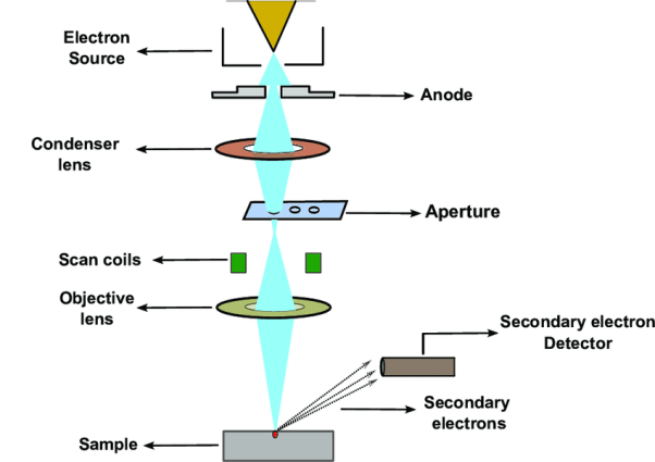
The beam travels through electromagnetic fields and lenses, which focus the beam down towards the sample. Once the beam hits the sample, electrons and X - rays are ejected from the sample. Detectors collect these X - rays, backscattered electrons and secondary electrons and convert them into a signal that is sent to a screen similar to a television screen. This produces the final image. In this research work, the powder samples were placed on the carbon tape which is attached to the sample holder.
The image formation in a scanning electron microscope is different from that in a conventional optical microscope. In SEM a focused mono-energetic electron beam scans the sample surface producing various "products" from the surface. These are secondary electrons, backscattered electrons and X-ray photons.
Advantages
- Advantages of a Scanning Electron Microscope include its wide-array of applications, the detailed three-dimensional and topographical imaging and the versatile information garnered from different detectors.
- SEMs are also easy to operate with the proper training and advances in computer technology and associated software make operation user-friendly.
- This instrument works fast, often completing SEI, BSE and EDS analyses in less than five minutes. In addition, the technological advances in modern SEMs allow for the generation of data in digital form.
- Although all samples must be prepared before placed in the vacuum chamber, most SEM samples require minimal preparation actions.
Disadvantages
- The disadvantages of a Scanning Electron Microscope start with the size and cost.
- SEMs are expensive, large and must be housed in an area free of any possible electric, magnetic or vibration interference.
- Maintenance involves keeping a steady voltage, currents to electromagnetic coils and circulation of cool water.
- Special training is required to operate an SEM as well as prepare samples.
- SEMs are limited to solid, inorganic samples small enough to fit inside the vacuum chamber that can handle moderate vacuum pressure.
- SEMs carry a small risk of radiation exposure associated with the electrons that scatter from beneath the sample surface.
Applications
- Scanning electron microscopy has been applied to the surface studies of metals, ceramics, polymers, composites and biological materials for both topography as well as compositional analysis.
- An extension of this technique is Electron Probe Micro Analysis (EPMA), where the emission of X-rays, from the sample surface, is studied upon exposure to a beam of high energy electrons.
- Depending on the type of detectors used this method is classified in to two as: Energy Dispersive Spectrometry (EDS) and Wavelength Dispersive Spectrometry (WDS). This technique is used extensively in the analysis of metallic and ceramic inclusions, inclusions in polymeric materials and diffusion profiles in electronic components.
Nano materials possess unique and beneficial, physical, chemical and mechanical properties; they can be used for a wide verity of applications.
Material technology
- Nanocrystalline aerogel are light weight and porous, so they are used for insulation in offices homes, etc.
- Cutting tools made of Nano crystalline materials are much harder, much more wear- resistance, and last stranger.
- Nano crystalline material sensors are used for smoke detectors, ice detectors on air craft wings, etc.
- Nano crystalline materials are used for high energy density storage batteries.
- Nano sized titanium dioxide and zinc dioxide is used in sunscreens to absorb and reflect ultraviolet rays.
- Nano coating of highly activated titanium dioxide acts as water repellent and antibacterial.
- The hardness of metals can be predominately enhanced by using nanoparticles.
- Nanoparticles in paints change colour in response to change in temperature or chemical environment, and reduce the infrared absorption and heat loss.
- Nano crystalline ceramics are used in automotive industry as high strength springs, ball bearings and valve lifters.
Information technology
- Nanoscale fabricated magnetic materials are used in data storage
- Nanocomputer chips reduce the size of the computer.
- Nano crystalline starting light emitting phosphors are used for flat panel displays.
- Nanoparticles are used for information storage.
- Nanophotonic crystals are used in chemical optical computers.
Biomedical
- Biosensitive nanomaterials are used for ragging of DNA and DNA chips.
- In the medical field, nanomaterials are used for disease diagnosis, drug delivery and molecular imaging.
- Nano crystalline silicon carbide is used for artificial heart valves due to its low weight and high strength.
Energy storage
- Nanoparticles are used hydrogen storage.
- Nano particles are used in magnetic refrigeration.
- Metal nanoparticles are useful in fabrication of ionic batteries.
- Nano materials possess unique and beneficial, physical, chemical and mechanical properties; they can be used for a wide verity of applications.
Material technology
- Nanocrystalline aerogel are light weight and porous, so they are used for insulation in offices homes, etc.
- Cutting tools made of Nano crystalline materials are much harder, much more wear- resistance, and last stranger.
- Nano crystalline material sensors are used for smoke detectors, ice detectors on air craft wings, etc.
- Nano crystalline materials are used for high energy density storage batteries.
- Nano sized titanium dioxide and zinc dioxide is used in sunscreens to absorb and reflect ultraviolet rays.
- Nano coating of highly activated titanium dioxide acts as water repellent and antibacterial.
- The hardness of metals can be predominately enhanced by using nanoparticles.
- Nanoparticles in paints change colour in response to change in temperature or chemical environment, and reduce the infrared absorption and heat loss.
- Nano crystalline ceramics are used in automotive industry as high strength springs, ball bearings and valve lifters.
Information technology
- Nanoscale fabricated magnetic materials are used in data storage
- Nanocomputer chips reduce the size of the computer.
- Nano crystalline starting light emitting phosphors are used for flat panel displays.
- Nanoparticles are used for information storage.
- Nanophotonic crystals are used in chemical optical computers.
Biomedical
- Biosensitive nanomaterials are used for ragging of DNA and DNA chips.
- In the medical field, nanomaterials are used for disease diagnosis, drug delivery and molecular imaging.
- Nano crystalline silicon carbide is used for artificial heart valves due to its low weight and high strength.
Energy storage
- Nanoparticles are used hydrogen storage.
- Nano particles are used in magnetic refrigeration.
- Metal nanoparticles are useful in fabrication of ionic batteries.