UNIT 4
Diode
TABLE OF CONTENTS
4.1 | Brief Review of Semiconductors and N-Type & P-Type Semiconductors |
4.2 | Formation of DepletionLayer in a PN Junction |
4.3 | Forward & Reverse Biased |
4.4 | V-I Characteristic |
4.5 | Diode CurrentEquation,Diode Applications |
4.6 | LED, Advantages & applications of LEDs and Seven-segment Displays |
A semiconductor is a substance whose resistivity lies between the conductors and insulators. The property of resistivity is not the only one that decides a material as a semiconductor, but it has few properties as follows.
- Semiconductors have the resistivity which is less than insulators and more than conductors.
- Semiconductors have negative temperature co-efficient. The resistance in semiconductors increases with the decrease in temperature and vice versa.
- The Conducting properties of Semiconductor changes, when a suitable metallic impurity is added to it, which is a very important property.
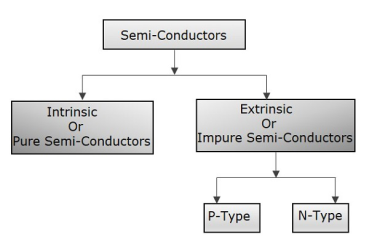
Semiconductor devices are extensively used in the field of electronics. The transistor has replaced the bulky vacuum tubes, from which the size and cost of the devices got decreased and this revolution has kept on increasing its pace leading to the new inventions like integrated electronics. The following illustration shows the classification of semiconductors.
Conduction in Semiconductors
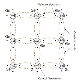
After having some knowledge on the electrons, we came to know that the outermost shell has the valence electrons which are loosely attached to the nucleus. Such an atom, having valence electrons when brought close to the other atom, the valence electrons of both these atoms combine to form “Electron pairs”. This bonding is not so very strong and hence it is a Covalent bond.
For example, a germanium atom has 32 electrons. 2 electrons in first orbit, 8 in second orbits, 18 in third orbits, while 4 in last orbit. These 4 electrons are valence electrons of germanium atom. These electrons tend to combine with valence electrons of adjoining atoms, to form the electron pairs, as shown in the following figure.
Creation of Hole:
Due to the thermal energy supplied to the crystal, some electrons tend to move out of their place and break the covalent bonds. These broken covalent bonds result in free electrons which wander randomly. But the moved away electrons create an empty space or valence behind, which is called as a hole.
This hole which represents a missing electron can be considered as a unit positive charge while the electron is considered as a unit negative charge. The liberated electrons move randomly but when some external electric field is applied, these electrons move in opposite direction to the applied field. But the holes created due to absence of electrons, move in the direction of applied field.
Hole Current
It is already understood that when a covalent bond is broken, a hole is created. Actually, there is a strong tendency of semiconductor crystal to form a covalent bond. So, a hole doesn’t tend to exist in a crystal. This can be better understood by the following figure, showing a semiconductor crystal lattice.
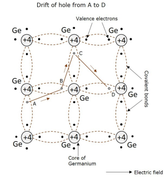
An electron, when gets shifted from a place A, a hole is formed. Due to the tendency for the formation of covalent bond, an electron from B gets shifted to A. Now, again to balance the covalent bond at B, an electron gets shifted from C to B. This continues to build a path. This movement of hole in the absence of an applied field is random. But when electric field is applied, the hole drifts along the applied field, which constitutes the hole current. This is called as hole current but not electron current because, the movement of holes contribute the current flow.
Electrons and holes while in random motion, may encounter with each other, to form pairs. This recombination results in the release of heat, which breaks another covalent bond. When the temperature increases, the rate of generation of electrons and holes increase, thus rate of recombination increases, which results in the increase of densities of electrons and holes. As a result, conductivity of semiconductor increases and resistivity decreases, which means the negative temperature coefficient.
Intrinsic Semiconductors
A Semiconductor in its extremely pure form is said to be an intrinsic semiconductor. The properties of this pure semiconductor are as follows −
- The electrons and holes are solely created by thermal excitation.
- The number of free electrons is equal to the number of holes.
- The conduction capability is small at room temperature.
In order to increase the conduction capability of intrinsic semiconductor, it is better to add some impurities. This process of adding impurities is called as Doping. Now, this doped intrinsic semiconductor is called as an Extrinsic Semiconductor.
Doping:
The process of adding impurities to the semiconductor materials is termed as doping. The impurities added, are generally pentavalent and trivalent impurities.
Pentavalent Impurities:
- The pentavalent impurities are the ones which has five valence electrons in the outer most orbits.
- Example: Bismuth, Antimony, Arsenic, Phosphorus
- The pentavalent atom is called as a donor atom because it donates one electron to the conduction band of pure semiconductor atom.
Trivalent Impurities:
- The trivalent impurities are the ones which has three valence electrons in the outer most orbits. Example: Gallium, Indium, Aluminum, Boron
- The trivalent atom is called as an acceptor atom because it accepts one electron from the semiconductor atom.
Extrinsic Semiconductor:
An impure semiconductor, which is formed by doping a pure semiconductor, is called as an extrinsic semiconductor. There are two types of extrinsic semiconductors depending upon the type of impurity added. They are N-type extrinsic semiconductor and P-Type extrinsic semiconductor.
N-Type Extrinsic Semiconductor:
A small amount of pentavalent impurity is added to a pure semiconductor to result in Type extrinsic semiconductor. The added impurity has 5 valence electrons.
For example, if Arsenic atom is added to the germanium atom, four of the valence electrons get attached with the Ge atoms while one electron remains as a free electron. This is as shown in the following figure.
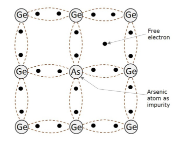
All of these free electrons constitute electron current. Hence, the impurity when added to pure semiconductor provides electrons for conduction.
- In N-type extrinsic semiconductor, as the conduction takes place through electrons, the electrons are majority carriers and the holes are minority carriers.
- As there is no addition of positive or negative charges, the electrons are electrically neutral.
- When an electric field is applied to an N-type semiconductor, to which a pentavalent impurity is added, the free electrons travel towards positive electrode. This is called as negative or N-type conductivity.
P-Type Extrinsic Semiconductor:
A small amount of trivalent impurity is added to a pure semiconductor to result in P-type extrinsic semiconductor. The added impurity has 3 valence electrons. For example, if Boron atom is added to the germanium atom, three of the valence electrons get attached with the Ge atoms, to form three covalent bonds. But, one more electron in germanium remains without forming any bond. As there is no electron in boron remaining to form a covalent bond, the space is treated as a hole. This is as shown in the following figure.
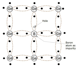
The boron impurity when added in a small amount provides a number of holes which helps in the conduction. All of these holes constitute hole current.
- In P-type extrinsic semiconductor, as the conduction takes place through holes, the holes are majority carriers while the electrons are minority carriers.
- The impurity added here provides holes which are called as acceptors, because they accept electrons from the germanium atoms.
- As the number of mobile holes remains equal to the number of acceptors, the Type semiconductor remains electrically neutral.
- When an electric field is applied to a P-type semiconductor, to which a trivalent impurity is added, the holes travel towards negative electrode, but with a slow pace than electrons. This is called as P-type conductivity.
- In this P-type conductivity, the valence electrons move from one covalent bond to another, unlike N-type.
Why Silicon is Preferred in Semiconductors?
Among the semiconductor materials like germanium and silicon, the extensively used material for manufacturing various electronic components is Silicon Si. Silicon is preferred over germanium for many reasons such as −
- The energy band gap is 0.7ev, whereas it is 0.2ev for germanium.
- The thermal pair generation is smaller.
- The formation of SiO2 layer is easy for silicon, which helps in the manufacture of many components along with integration technology.
- Si is easily found in nature than Ge.
- Noise is less in components made up of Si than in Ge.
Hence, Silicon is used in the manufacture of many electronic components, which are used to make different circuits for various purposes. These components have individual properties and particular uses.
There is a greater combination of holes in P-region and electrons in N-region. This difference in concentration establishes a density mismatch across the junction resulting in majority carrier diffusion. Holes diffuse from P to N and electrons from N to P regions causing the recombination.
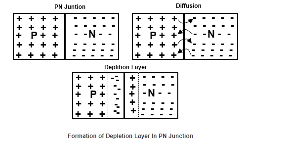
This recombination of electrons and holes produces a narrow region at junction called depletion region.
Potential Barrier:
As the depletion layer built up a different of potential appears across the junction this difference of potential at junction is called potential barrier. The value of potential barrier VB is 0.3 volt for germanium and 0.7 volts for silicon.
Forward Biased:
When we connect p-type region of a junction with the positive terminal of a voltage source and n-type region with the negative terminal of the voltage source, then the junction is said to be forward biased. At this condition, due to the attraction of positive terminal of source, electrons which participated in covalent bond creations in p-type material will be attracted towards the terminal.
As result numbers of covalent bonds are broken and, electrons are shifted towards the positive terminal. As a result, the concentration of electrons in the crystal nearer to the terminal increases and these electrons recombine with holes here. In this way, the number of holes increases in the portion of the p-type region away from the junction, and it is reduced in the portion of p-type region nearer to the terminal. As such holes are shifted from terminal to junction.
Due to the higher concentration of holes adjacent to negative impurity ions layer the electrons of negative ions come out and recombine with those holes and create new holes in the layer. Consequently, the width of this negative ions layer is reduced and finally this layer vanishes.
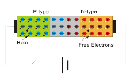
Similarly due to the negative terminal of source the free electrons in the n-type region will repeal towards junction where they will find the layer of positive impurity ions and start recombine with these ions and generate free electrons inside the layer. Consequently, the width of positive impurity ions is reduced, and finally, it vanishes.
In these ways, both layers of ions disappear, and there will be no more depletion layer. After the depletion layer disappeared, free electrons from the n-type region can easily drift to p-type region and holes from p-type region to n-type region in the crystal. Hence, ideally there will be no obstruction of flowing current and the pn junction behaves as the short circuit.
Reverse Biased:
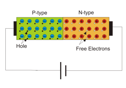
When positive terminal of a voltage source is connected to the n-type region and the negative terminal of the source is connected to the p-type region then the pn junction is said to be in reverse biased condition. When there is no voltage applied across the p n junction, the potential developed across the junction is 0.3 volts at 25oC for germanium pn junction and 0.7 volts at 25oC for silicon p n junction.
The polarity of this potential barrier is same as the polarity of voltage source applied during reverse biased condition. Now if reverse biased voltage across the pn junction is increased the barrier potential developed across the pn junction is also increased. Hence, the pn junction is widened.
When positive terminal of the source is connected to the n-type region, the free electrons of that region are attracted towards positive terminal of the source because of that more positive impurity ions are created in the depletion layer which makes the layer of positive impurity ions thicker.
At the same time since negative terminal of the source is connected to the p-type region of the junction, electrons are injected in this region. Due to the positive potential of the n-type region the electrons are drifted towards the junction and combine with holes adjacent to the layer of positive impurity ions and create more positive impurity ions in the layer. Hence, the thickness of the layer increases.
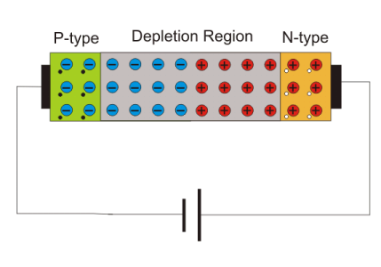
In this way over all width of the depletion layer increases along with its barrier potential. This increment of the width of depletion layer will continue till the barrier potential reaches to applied reverse biased voltage. Although this increment of barrier potential will continue up to applied reverse biased voltage but if the applied reverse biased voltage is sufficiently high then the depletion layer will disappear due zener breakdown and avalanche breakdowns.
It is also to be noted that after completion of reverse biased depletion layer there is no more drift of charge carriers (electrons and holes) through the junction as the potential barrier opposes the applied voltage which has the same value as the potential barrier. Although tiny current flow from n-type region to p-type region due to minority carriers that is thermally generated electrons in p-type semiconductor and holes in n-type semiconductor.
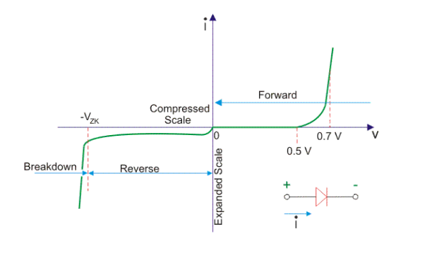
In the forward bias, the operational region is in the first quadrant. The threshold voltage for Germanium is 0.3 V and for Silicon is 0.7 V. Beyond this threshold voltage the graph goes upward in a non linear manner. This graph is for the dynamic Resistance of the junction in the forward bias.
In the reverse bias the voltage increases in the reverse direction across the p-n junction, but no current due to the majority carriers, only a very small leakage current flows. But at a certain reverse voltage p-n junction breaks in conduction. It is only due to the minority carriers. This amount of voltage is sufficient for these minority carriers to break the depletion region. At this situation sharp current will flow through this junction. This breakdown of voltage is of two types.
Avalanche Breakdown: it is not properly sharp, rather inclined linear graph i.e. after break down small increase in reverse voltage causes more sharp current gradually.
Zener Breakdown: This breakdown is sharp and no need to increase reverse bias voltage to get more current, because current flows sharply.
Diode Equivalent Circuits:
Diode is an active element in electrical circuit it has some resistance and some value of junction capacitance when the diode in circuit is replaced by same value of the resistance and capacitance it’s called as the Diode equivalent circuit.
To define the dc diode model, we look at the characteristics of an ideal diode and the modifications that were required due to practical considerations. To review: ¾ Ideal diode: VON = 0, Rr = ∞ and Rf = 0. In other words, the ideal diode is a short in the forward bias region and an open in the reverse bias region. ¾ Practical diode (silicon): VON = 0.7V, Rr < ∞ (typically several MΩ), Rf ≈ rd (typically < 50 Ω). The general representation for a practical diode under dc operating conditions is shown below. Recall the diode is a two-terminal device, which simply means that it connects to other circuit elements at connection points labelled a and b in the circuit below with the voltage Vab applied across the diode. Note that the terminal voltage Vab is the same as the voltage applied across the diode, VD – same animal, different notation. This model may be simplified if we can define the operating region as forward or reverse bias. For the forward bias region (VD ≥ 0.7 V for silicon), the ideal diode is a short and the terminal characteristics of the model above reduce to the parallel combination of Rr and Rf. Since Rr >> Rf, Rr ||Rf ≈ Rf. Likewise, when the voltage applied to the diode is less than VON (VD< 0.7 V for silicon), the ideal diode is an open and the resistance between terminals a and b is Rr. These two cases are illustrated below for reference .

Forward biased DC model Reverse biased DC model
Even though the same, they behave very differently! Remember the values of the resistances in the different regions and you can see that diode characteristics in the forward and reverse bias regions are quite distinct.
Diode Characteristics:
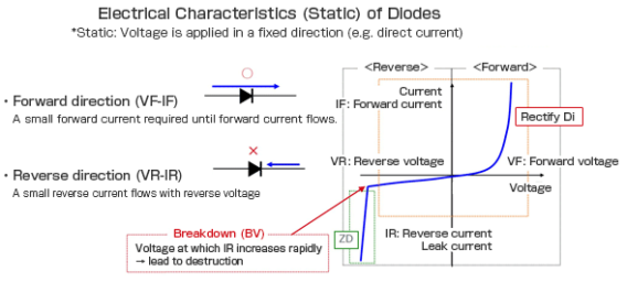
Basic static characteristics of diodes are the forward voltage VF and forward current IF, and the reverse voltage and current VR and IR.
The area surrounded by the orange dashed line in the diagram on the right indicates the usable area of rectifying diodes. Specifically, this is the area within the range of allowable IF, and within the breakdown voltage range in the reverse direction.
It should be noted that the area enclosed by the green dashed line is the usable area of Zener diodes, although these are not discussed in this chapter. This area isn’t usable for other diodes, and if this area is entered without any limits on the IR, device failure may occur.
Diode as a Switch:
Whenever a specified voltage is exceeded, the diode resistance gets increased, making the diode reverse biased and it acts as an open switch. Whenever the voltage applied is below the reference voltage, the diode resistance gets decreased, making the diode forward biased, and it acts as a closed switch.
The following circuit explains the diode acting as a switch.
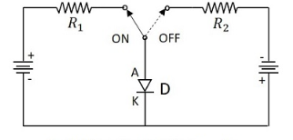
A switching diode has a PN junction in which P-region is lightly doped and N-region is heavily doped. The above circuit symbolizes that the diode gets ON when positive voltage forward biases the diode and it gets OFF when negative voltage reverse biases the diode.
As the forward current flows till then, with a sudden reverse voltage, the reverse current flows for an instance rather than getting switched OFF immediately. The higher the leakage current, the greater the loss. The flow of reverse current when the diode is reverse biased suddenly may sometimes create few oscillations, called RINGING.
This ringing condition is a loss and hence should be minimized. To do this, the switching times of the diode should be understood.
Diode as a Rectifier (half-wave & full-wave):
A complete half-wave rectifier circuit consists of 3 main parts:
- A transformer
- A resistive load
- A diode
A half wave rectifier circuit diagram looks like this:
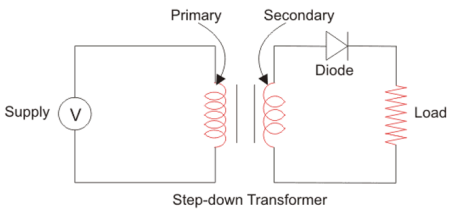
First, a high AC voltage is applied to the to the primary side of the step- down transformer and we will get a low voltage at the secondary winding which will be applied to the diode.

During the positive half cycle of the AC voltage, the diode will be forward biased and the current flows through the diode. During the negative half cycle of the AC voltage, the diode will be reverse biased and the flow of current will be blocked. The final output voltage waveform on the secondary side (DC) is shown in figure above.
If we replace the secondary transformer coils with a source voltage, we can simplify the circuit diagram of the half-wave rectifier as:
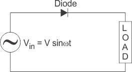
For the positive half cycle of the AC source voltage, the equivalent circuit effectively becomes:
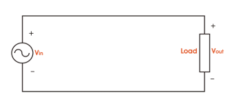
This is because the diode is forward biased, and is hence allowing current to pass through. So, we have a closed circuit.
But for the negative half cycle of the AC source voltage, the equivalent circuit becomes:
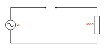
Because the diode is now in reverse bias mode, no current is able to pass through it. As such, we now have an open circuit. Since current cannot flow through to the load during this time, the output voltage is equal to zero.
This all happens very quickly – since an AC waveform will oscillate between positive and negative many times each second (depending on the frequency).
Here’s what the half wave rectifier waveform looks like on the input side (Vin), and what it looks like on the output side (Vout) after rectification (i.e. conversion from AC to DC):
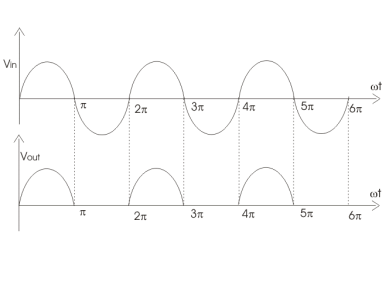
The graph above actually shows a positive half wave rectifier. This is a half-wave rectifier which only allows the positive half-cycles through the diode, and blocks the negative half-cycle.
The voltage waveform before and after a positive half wave rectifier is shown in figure 4 below.

Conversely, a negative half-wave rectifier will only allow negative half-cycles through the diode and will block the positive half-cycle. The only difference between a positive and negative half wave rectifier is the direction of the diode.
As you can see in figure 5 below, the diode is now in the opposite direction. Hence the diode will now be forward biased only when the AC waveform is in its negative half cycle.

ADVANTAGES:-
1) Simple Construction.
2) Component required less.
3) Small size.
APPLICATION:-
Walkman, low-cost power supply.
TRANSFORMER UTILISATION FACTOR (TUF): It indicates how well the ilp transformer is being utilized
TUF= DC O/P Power / AC power rating of the transformer

Full wave rectifier:
1) A center-tapped rectifier is a type of full-wave rectifier that uses two diodes connected to the secondary of a center-tapped transformer.
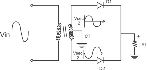
Center tapped full wave rectifier operation:-
I) during the positive half cycle of the i/p ac supply.
Diagram

D1.Is in forward biased & D2 is in reverse biased.
II) During -ve half cycle.

D1 Reverse biased
D2 Forward biased
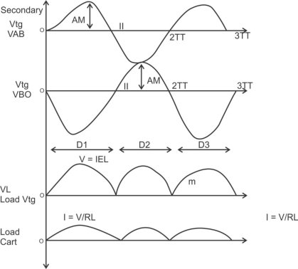
ADVANTAGES
- Law ripple factor as Compared to HKR.
- Better rectification efficiency.
- Better TUF.
- A higher value of average load vtg&avg load crt.
- No possibility of transformer core saturation.
DISADVANTAGES
PIV of the diode is 2vm, more size costly.
APPLICATION
I) Battery charges.
2) Power supply at the laboratory, high current, electronic ckt.
Capacitor filter:
A typical capacitor filter circuit diagram is shown below. The designing of this circuit can be done with a capacitor C as well as load resistor (RL). The rectifier’s exciting voltage is given across the terminals of a capacitor. Whenever the voltage of the rectifier enhances then the capacitor will be charged as well as supplies the current to the load.
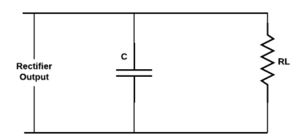
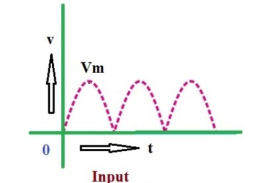
At the last part of the quarter phase, the capacitor will be charged to the highest rectifier voltage value that is denoted with Vm, and then the voltage of the rectifier starts to reduce. As this happens, the capacitor starts discharging through the voltage across it and load. The voltage across the load will reduce little only because the next peak voltage occurs instantaneously to charge the capacitor. This procedure will repeat many times and the output waveform will be seen that very slight ripple is missing in the output. Furthermore, the output voltage is superior because it remains significantly close to the highest value of the output voltage of the rectifier.
PHOTODIODE:
The photodiode is a p-n junction semiconductor diode which is always operated in the reverse biased condition.
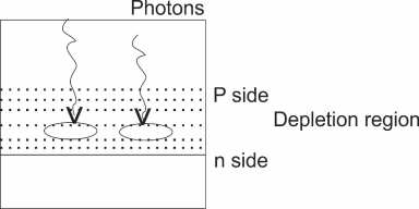
The light is always focused through a glass lens on the junction of the photodiode As the photodiode is reverse biased the depletion region is quite wide, penetrated on both sides of the junction.
The photons incident on the depletion region will impact their energy to the Ions present in the depletion region and generates e hole pairs.
The photons incident on the depletion region, so the number of electron hole pairs will be generated, depends on the intensity of light [number of photons] These and holes will be attracted towards the +ve& -ve terminals respectively of the photocurrent.
With an increase in the light intensity more number of e hole pairs are generated and the photocurrent increases thus the photocurrent is proportional to the light intensity.
LED:
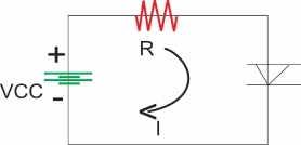
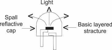
- An LED emits light when electrical energy is applied to it. For proper operation, it is necessary to forward bias the LED.
Construction of LED:-
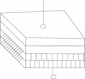
To make the emission of light in one direction cup type construction is used for LED.
PRINCIPLE LED OPERATION:
When the led is forward biased the electrons in the n-region will cross the junction and recombine with the holes in the p-type material.
These free e- reside in the conduction band & hence at a higher energy level than the holes in the valence band
When recombination takes place this e- return peak to the valence bandwhich is at a lower energy level than the conduction band.
While returning back the recombining e-give away the excess energy in the form of light. This process is called electroluminescence. In this way an LED emits light.
Colour of the Emitted Light:
Material Use Color of Emitted Light:
i) Gallium Arsenide (GOAS) in fared (IR)
Ii) GaASP (gallium arsenide Red or Yellow
Phosphide)
Iii) Gallium phosphide (GAP) Red or Green
Application :
Used in 7 Segment Display