UNIT 5
Transistor
TABLE OF CONTENTS
5.1 | BJT Construction |
5.2 | Junction Biasing of BJT |
5.3 | Operation of NPN & PNP BJT |
5.4 | Input and Output Characteristics of Transistor in CE configuration |
5.5 | Transistor as an Amplifier& as a Switch |
5.6 | Advantages of ICs & Scale of Integration |
*BJT:-The BJT is constructed with the three draped semiconductors region’s separate by two Pn junctions as shown below
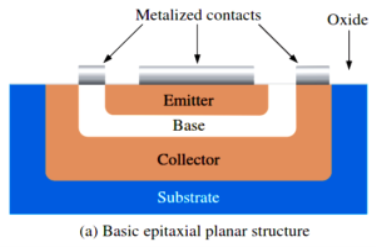
-Basic epitaxial planner structures.
-Three terminal with region’s are called emitter, base and collector.
-The physical representation of the two types of BJT’s,
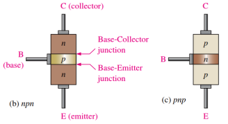
One type consists between two regions separated by a P region (NPN) and other type consists of two p regions separated by an n region (PnP).
-The Pn junction joining the base region and the emitter region is called the base emitter junction.
-The Pn junction joining the base region and the collector region is called the base collector junction.
-The base region is lightly doped and very thin compared to the heavily doped emitter and the moderately doped collector regions.
Base Transistor Operation:-
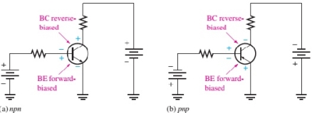
In order for the transistor to operate properly as an amplifier the two Pn junctions must be correctly biased with the external D.C vtg.
-The next figure shows the proper bias arrangement for both the NPN and PnP transistors for active operation as an amplifier.
-In both the cases the base emitter
(BE) junction is forward biased & the base collector junction (BC) junction is reverse biased
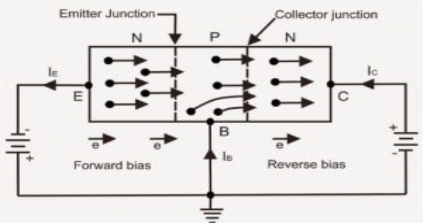
- As from above figure consider n-p-n transistor. The forward bias from base to emitter narrow’s the BE depletion region and the reverse bias from base to collector widens the BC depletion region shown in figure.
- The heavily doped N-TYPE emitter region is full with conduction band(frep) electron’s that easily diffuse through the forward biased BE junction into the p-type base region where they become minority carrier’s same as forward biased diode region
- The base region is lightly doped & very thin so that it has a very limited number of holes.
- Those only a small percentage of all the e-flowing the BE junction can combine with the available holes in the base.
- The relatively few recombined flow out of the base lead as valance electrons, forming as small base current.
- Most of the e flowing from the emitter into the thin lightly dooped base region do not recombine but diffuse into the BC depletion region.
- The BC depletion region diffuse e is being pulled across the reverse biased BC junction by the attraction of the collector supply vtg.
- The electrons now move through the collector region, out through the collector lead into the +ve terminal of the collector vtg source. This forms the collector electrons current.
- The collector current is much larger than the base current.
- This is the reason transistor exhibit current gain.
Transistor Current:-
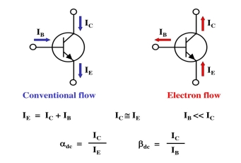
Transistor’s Characteristic’s and parameters:-
-The transistors is connected to d.c bias vtg for both the npn & pnp types VBB forward biases the base emitter junction & Vcc reverse biases the base collector junction.
*Biasing conditions for different regions of operation:-
Sr. No | Region of operation | BE junction | CB junction | Work |
1 | Cut off region | R.B | R.B | S/w |
2 | Active region | F.B | R.B | Ampr |
3 | Saturation region | F.B | F.B |
|
Transistor’s Configuration:-
1) Common Base configuration(C.B)
2) Common emitter Configuration(C.E)
3) Common Collector Configuration(C.C)
Common Base configuration (C.B):-

-The I/p is applied between the emitter and the base. The base acts as a common terminal between the I/p and o/p.
-The input vtg is therefore VEB and the input current is IE.
-The output is taken between the collector and the base therefore the output vtg is VCB and the output current is IC.
* Current relation’s in CB configuration:-
-The collector current is IC of the common base configuration is given by
IC=IC (INI) + ICBO
-Where the Ic (INI) called the injected collectors current and it is due to the number of electrons crossing the collectors base junction.
-ICBO: - This is the reverse saturation current flowing due to the minority carrier’s between the collector and base when the emitter is open
-ICBO flow’s due to the reverse biased collector’s base junction. As ICBO negligible as compared to Ic (INI) we can neglect it in practice.
.’. IC =Ic (INI)………………………practically
IC =ICBO………………with emitter open
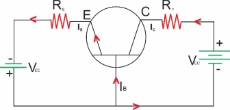
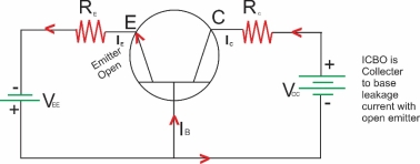
 Emitter is open
 ICBO
ICBO
Collector is to base control
-Since the ICBO flow’s due to terminally generated minority carrier’s it increases with increase the temperature.
-It doubles its value for every 100c rise in temperature.
-Current amplification factor or current gain (ddc):-
Current amplification factor or current gain is the ratio of collector current due to the injection to the total emitter current
αd.c = Ic (INI)
-The value of the ddc for CB configuration will always be less than 1.This is because
IC (INI) <IE.
-Typically the value of d.d.c ranges between the 0.95 to 0.995 depending upon the thickness of the base region.
-Larger the thickness of the base region smaller the value of the d.d.c
Ic (INI) =d.d.c.IE
Hence the expression for IC is given by
IC=αd.c IE + ICBo --------------------I
But the ICBo is negligibly small
IC d.d.c IE
* Expression for IB:-
IE=IB+IC
IE=αd.cIE+ICBo+IB…………………from I
IB= (1-αd.c) IE-ICBo
Neglecting ICBo
IB= (1-αd.c) IE
- Characteristics of a transistors in a common base configuration:-
1. Input Characteristic:-
A. Input Characteristic: is always a graph of input current verses input vtg. For common base (CB) configuration input current is the emitter current (IE) & I/p vtg. Is the emitter to the base vtg (VEB)
The I/p Characteristic is plotted at a constant O/p vtg. VCB

B. Output Characteristic:
Output Characteristic is always a graph of O/p current versus O/p Vtg.
For the CB configuration the O/p current is collector current (IC) of the output voltage is collector to base vtg. (VCB)
Output Characteristic is plotted for a constant value of me /p current (IE)
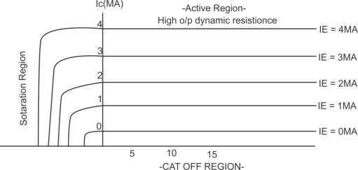
O/p Characteristic of an n-p-n transistor in CB Configuration
Dynamic O/p resistance (ro)
Ro =  / I
/ I  constant
In the active region Ic does not depend on VCB. It depends only on the I/p current IE. That is why the transistor is called as a current controlled or current operated device.
Feature of CB Configuration:
- Common terminal : base
- Input current : IE
- O/p current IC
- I/P Vtg. : VEB
- O/P Vtg. VCB
- Current gain :
 ( less than 1)
 - Vtg. Gain : medium
- Input resistance : very low (20-)
- O/P resistance : very high (1 m-2)
- Application : as preamplifier
The three types of configurations are Common Base, Common Emitter and Common Collector configurations. In every configuration, the emitter junction is forward biased and the collector junction is reverse biased.
Common Base CB
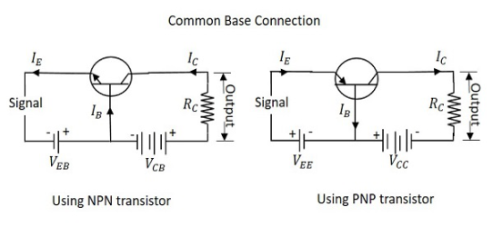
The name itself implies that the Base terminal is taken as common terminal for both input and output of the transistor. The common base connection for both NPN and PNP transistors is as shown in the following figure.
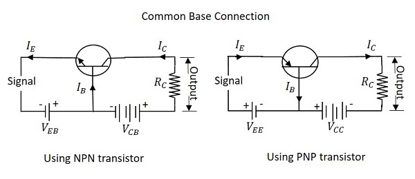
For the sake of understanding, let us consider NPN transistor in CB configuration. When the emitter voltage is applied, as it is forward biased, the electrons from the negative terminal repel the emitter electrons and current flows through the emitter and base to the collector to contribute collector current. The collector voltage VCB is kept constant throughout this.
In the CB configuration, the input current is the emitter current IE and the output current is the collector current IC.
Current Amplification Factor α
The ratio of change in collector current ΔIC to the change in emitter current ΔIE when collector voltage VCB is kept Constant is called as Current amplification factor. It is denoted by α.
α=ΔIC/ΔIE at constant VCB
Expression for Collector current
Along with the emitter current flowing, there is some amount of base current IB which flows through the base terminal due to electron hole recombination. As collector-base junction is reverse biased, there is another current which is flown due to minority charge carriers. This is the leakage current which can be understood as Ileakage. This is due to minority charge carriers and hence very small.
The emitter current that reaches the collector terminal is
α IE
Total collector current
IC=αIE+Ileakage
If the emitter-base voltage VEB = 0, even then, there flows a small leakage current, which can be termed as ICBO collector−basecurrentwithoutputopencollector−basecurrentwithoutputopen.
The collector current therefore can be expressed as
IC=αIE+ICBO
IE=IC+IB
IC=α(IC+IB) +ICBO
IC (1−α) =αIB+ICBO
IC= (α1−α) IB + (ICBO1−α)
IC= (α1−α) IB+ (11−α) ICBO
Hence the above derived is the expression for collector current. The value of collector current depends on base current and leakage current along with the current amplification factor of that transistor in use.
Characteristics of CB configuration
- This configuration provides voltage gain but no current gain.
- Being VCB constant, with a small increase in the Emitter-base voltage VEB, Emitter current IE gets increased.
- Emitter Current IE is independent of Collector voltage VCB.
- Collector Voltage VCB can affect the collector current IC only at low voltages, when VEB is kept constant.
- The input resistance ri is the ratio of change in emitter-base voltage ΔVEB to the change in emitter current ΔIE$ at constant collector base voltage VCB.
η=ΔVEB/ΔIE at Constant VCB
- As the input resistance is of very low value, a small value of VEB is enough to produce a large current flow of emitter current IE.
- The output resistance ro is the ratio of change in the collector base voltage $ΔVCB$$ΔVCB$ to the change in collector current ΔIC at constant emitter current IE.
Ro ΔVCB/ΔIC at Constant lE
- As the output resistance is of very high value, a large change in VCB produces a very little change in collector current IC.
- This Configuration provides good stability against increase in temperature.
- The CB configuration is used for high frequency applications.
Common Emitter CE
The name itself implies that the Emitter terminal is taken as common terminal for both input and output of the transistor. The common emitter connection for both NPN and PNP transistors is as shown in the following figure.
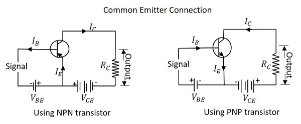
Just as in CB configuration, the emitter junction is forward biased and the collector junction is reverse biased. The flow of electrons is controlled in the same manner. The input current is the base current IB and the output current is the collector current IC here.
Base Current Amplification factor β
The ratio of change in collector current ΔIC to the change in base current ΔIB is known as Base Current Amplification Factor. It is denoted by β
β=ΔICΔ/IB
Relation between β and α
Let us try to derive the relation between base current amplification factor and emitter current amplification factor.
β=ΔIC/ΔIB
α=ΔIC/ΔIE
IE=IB+IC
ΔIE=ΔIB+ΔIC
ΔIB=ΔIE−ΔIC
We can write
β=ΔIC/ΔIE−ΔIC
Dividing by ΔIE
β=ΔIC/ΔIE/ΔIE/ΔIE−ΔIC/ΔIE
We have
α=ΔIC/ΔIE
Therefore,
β=α/1−α
From the above equation, it is evident that, as α approach 1, β reaches infinity.
Hence, the current gain in Common Emitter connection is very high. This is the reason this circuit connection is mostly used in all transistor applications.
Expression for Collector Current
In the Common Emitter configuration, IB is the input current and IC is the output current.
We know
IE=IB+IC
And
IC=αIE+ICBO
=α (IB+IC) +ICBO
IC (1−α) =αIB+ICBO
IC=α/1−α IB+1/1−α ICBO
If base circuit is open, i.e. if IB = 0,
The collector emitter current with base open is ICEO
ICEO=1/1−αICBO
Substituting the value of this in the previous equation, we get
IC=α/1−α . IB+ ICEO
IC=βIB +ICEO
Hence the equation for collector current is obtained.
Knee Voltage
In CE configuration, by keeping the base current IB constant, if VCE is varied, IC increases nearly to 1v of VCE and stays constant thereafter. This value of VCE up to which collector current IC changes with VCE is called the Knee Voltage. The transistors while operating in CE configuration, they are operated above this knee voltage.
Characteristics of CE Configuration
- This configuration provides good current gain and voltage gain.
- Keeping VCE constant, with a small increase in VBE the base current IB increases rapidly than in CB configurations.
- For any value of VCE above knee voltage, IC is approximately equal to βIB.
- The input resistance ri is the ratio of change in base emitter voltage ΔVBE to the change in base current ΔIB at constant collector emitter voltage VCE.
Ri =ΔVBE/ΔIB at constant VCE
- As the input resistance is of very low value, a small value of VBE is enough to produce a large current flow of base current IB.
- The output resistance ro is the ratio of change in collector emitter voltage ΔVCE to the change in collector current ΔIC at constant IB.
Ro=ΔVCE/ΔIC at constant IB
- As the output resistance of CE circuit is less than that of CB circuit.
- This configuration is usually used for bias stabilization methods and audio frequency applications.
Common Collector CC Configuration
The name itself implies that the Collector terminal is taken as common terminal for both input and output of the transistor. The common collector connection for both NPN and PNP transistors is as shown in the following figure.
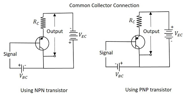
Just as in CB and CE configurations, the emitter junction is forward biased and the collector junction is reverse biased. The flow of electrons is controlled in the same manner. The input current is the base current IB and the output current is the emitter current IE here.
Current Amplification Factor γ
The ratio of change in emitter current ΔIE to the change in base current ΔIB is known as Current Amplification factor in common collector CC configuration. It is denoted by γ.
γ=ΔIE/ΔIB
- The current gain in CC configuration is same as in CE configuration.
- The voltage gain in CC configuration is always less than 1.
Relation between γ and α
Let us try to draw some relation between γ and α
γ=ΔIE/ΔIB
α=ΔIC/ΔIE
IE=IB+IC
ΔIE=ΔIB+ΔIC
ΔIB=ΔIE−ΔIC
Substituting the value of IB, we get
γ=ΔIE/ΔIE−ΔIC
Dividing by ΔIEΔIE
γ=ΔIE/ΔIE/ΔIE/ΔIE−ΔIC/ΔIE
1/1−α1
γ=1/1−α
Expression for collector current
We know
IC=αIE + ICBOIC=αIE+ICBO
IE=IB+IC=IB+ (αIE+ICBO) IE=IB+IC=IB+ (αIE+ICBO)
IE (1−α) =IB+ICBOIE (1−α) = IB+ICBO
IE=IB1−α+ICBO1−αIE=IB1−α+ICBO1−α
IC≅IE= (β+1) IB + (β+1) ICBO
The above is the expression for collector current.
Characteristics of CC Configuration
- This configuration provides current gain but no voltage gain.
- In CC configuration, the input resistance is high and the output resistance is low.
- The voltage gain provided by this circuit is less than 1.
- The sum of collector current and base current equals emitter current.
- The input and output signals are in phase.
- This configuration works as non-inverting amplifier output.
- This circuit is mostly used for impedance matching. That means, to drive a low impedance load from a high impedance source.
Definition:
The configuration in which the emitter is connected between the collector and base is known as a common emitter configuration. The input circuit is connected between emitter and base, and the output circuit is taken from the collector and emitter. Thus, the emitter is common to both the input and the output circuit, and hence the name is the common emitter configuration. The common emitter arrangement for NPN and PNP transistor is shown in the figure below.
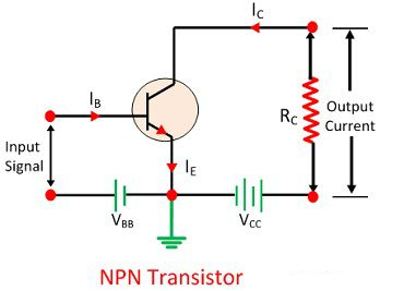
Base Current Amplification Factor (β)
The base current amplification factor is defined as the ratio of the output and input current in a common emitter configuration. In common emitter amplification, the output current is the collector current IC, and the input current is the base current IB.
In other words, the ratio of change in collector current with respect to base current is known as the base amplification factor. It is represented by β (beta).
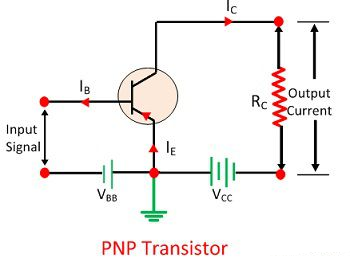
Base Current Amplification Factor (β):
The base current amplification factor is defined as the ratio of the output and input current in a common emitter configuration. In common emitter amplification, the output current is the collector current IC, and the input current is the base current IB.
In other words, the ratio of change in collector current with respect to base current is known as the base amplification factor. It is represented by β (beta).

Relation between Current Amplification Factor (α) & Base Amplification Factor (β):
The relation between Β and α can be derived as
We Known,
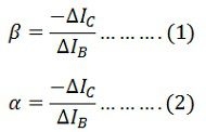
Now,
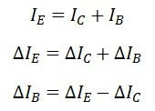
Substituting the value of ΔIE in equation (1), we get,
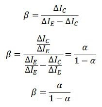
The above equation shows that the when the reaches to unity, then the β reaches to infinity. In other words, the current gain in a common emitter configuration is very high, and because of this reason, the common emitter arrangement circuit is used in all the transistor applications.
Collector Current:
In CE configuration, the input current IB and the output current IC are related by the equation shown below.
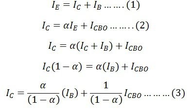
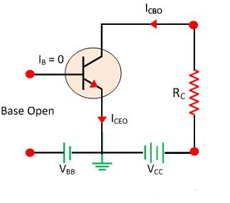
If the base current is open (i.e., IB = 0). The collector current is current to the emitter, and this current is abbreviated as ICEO that means collector- emitter current with the base open.

Substitute the value ΔIB in equations (1), we get,

Characteristics of Common emitter (CE) Configuration:
The characteristic of the common emitter transistor circuit is shown in the figure below. The base to emitter voltage varies by adjusting the potentiometer R1. And the collector to emitter voltage varied by adjusting the potentiometer R2. For the various setting, the current and voltage are taken from the milli ammeters and voltmeter. On the basis of these readings, the input and output curve plotted on the curve.
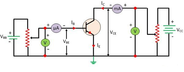
Input Characteristic Curve:
The curve plotted between base current IB and the base-emitter voltage VEB is called Input characteristics curve. For drawing the input characteristic the reading of base currents is taken through the ammeter on emitter voltage VBE at constant collector-emitter current. The curve for different value of collector-base current is shown in the figure below.
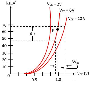
The curve for common base configuration is similar to a forward diode characteristic. The base current IB increases with the increases in the emitter-base voltage VBE. Thus the input resistance of the CE configuration is comparatively higher that of CB configuration.
The effect of CE does not cause large deviation on the curves, and hence the effect of a change in VCE on the input characteristic is ignored.
Input Resistance:
The ratio of change in base-emitter voltage VBE to the change in base current ∆IB at constant collector-emitter voltage VCE is known as input resistance, i.e.

Output Characteristic:
In CE configuration the curve draws between collector current IC and collector-emitter voltage VCE at a constant base current IB is called output characteristic. The characteristic curve for the typical NPN transistor in CE configuration is shown in the figure below.
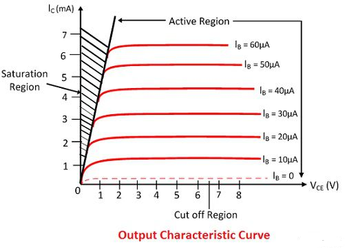
In the active region, the collector current increases slightly as collector-emitter VCE current increases. The slope of the curve is quite more than the output characteristic of CB configuration. The output resistance of the common base connection is more than that of CE connection.
The value of the collector current IC increases with the increase in VCE at constant voltage IB, the value β of also increases.
When the VCE falls, the IC also decreases rapidly. The Collector-base junction of the transistor is always in forward bias and work saturate. In the saturation region, the collector current becomes independent and free from the input current IB
In the active region IC = βIB, a small current IC is not zero, and it is equal to reverse leakage current ICEO.
Output Resistance:
The ratio of the variation in collector-emitter voltage to the collector-emitter current is known at collector currents at a constant base current IB is called output resistance ro.

The value of output resistance of CE configuration is more than that of CB.
Common Emitter (CE) configuration
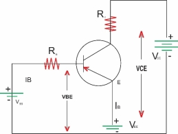
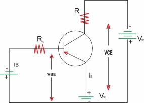
The important points about the CE
Configurations are as follows: the emitter acts as a common terminal between me /p and output. The /p Vtg. Is called between base and emitter
Hence VBE is the I/p Vtg. And IB is the input current.
The O/p is taken between the collector and emitter. There for VCE is the O/p Vtg. And IC is the O/p current.
In order to operate the transistor in its active region the base emitter (BE) junction is forward biased and collector base junction is reverse biased.
- Current relations in CE Configuration:
IE = IC + IB
Where IC =  d.c.IE + ICBO
Rearrange this eqn to get
IC – ICBO =  d.c.IE
 -
-  = IE = IC + IB
 ] = IB -
IC ] = IB +
 ] +
] + 
- Current gain
 : as
: as  is the ration of o/p current TC and I/p current IB it called common emitter current amplification factor or simply current gain. Thus transistor acts as current amplifier.
The value of  is match higher than
 =
= 
 =
=  =
=  =
= 
IC =  IB +
IB +  …….. I
But  =
= 
 1 +
1 +  =
=  + 1
+ 1
1 +  =
= 
 1 +
1 +  =
= 
Put in eqn I
IC =  IB + (1+
 ICBO above eqn can be expressed as
IC =  IB + ICEO
Where ICEO is the reverse saturation current for the CE configuration which is given by
ICEO = (1+ ) ICBO
- Reverse leakage current :
The Reverse leakage current of a transistor operating
In the LE configuration is denoted by
ICEO = (1 + ) ICBO
As the value of 
- Match greater than 1 ICEO>>>> ICBO
- As IC =

Put IB = 0
 IC = (1 +
The Reverse leakage current (ICEO)
Increases with increase in the temperature this current flows in the same direction as that of IC there for the collector current IC will increase with increase in temperature even when IB is constant
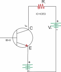
This is called as thermal instability so in CE configuration thermal stabilizing CKT must be included.
- Relation between IC and IB (Current gain
 )
)
We know that
IC 
Though ICEO is large it is much smaller as compared to . Therefor the eqn for IC gets modified as
 C =
C = 

- Relation betn
 &
& :
:
We know that
 but
but 
 =
=  =
= 
 =
= 
Similarly we can obtain the expression for  d.c in terms of
  as follows
 d.c =
d.c =  but
but 
=
Multiply & divide numerator & denominator for by IE
 d.c =
d.c = 
 d.c =
d.c = 
 =
= 
- Impact characteristics :
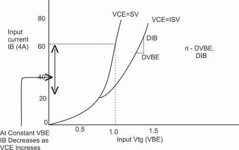
The value of dynamic input resistance ri is low for the CE configuration but it is not as low as that of CE configuration
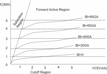
- Cutoff region: Both the BE & CB junctions are reverse biased to operate the transistor in cutoff region. The base current IB = 0 & the collector current is equal to the reverse leakage ICEO. The region below the characteristics for
IB = 0 is cutoff region.
- Active region : the BE emitter junction is forward biased CB junction is reverse biased to operate the transistor in the active region
The collector current IC increases slightly with increase in the vtg. VCE. However the collector current is largely dependent on the base current IB
At fixed value of VCE if IB is increased then it will cause IC to increase substantially.
This is because IC = BIB this relation is true only for the active region of operation.
- Saturation region : the BE junction as well as the collector junction must be forward biased to operate the transistor in its saturation region
- Dynamic o/p resistance
 / constant IB
1. Extremely small size – Thousands times smaller than discrete circuits. It is because of fabrication of various circuit elements in a single chip of semiconductor material.
2. Very small weight owing to miniaturised circuit.
3. Very low cost because of simultaneous production of hundreds of similar circuits on a small semiconductor wafer. Owing to mass production of an IC costs as much as an individual transistor.
4. More reliable because of elimination of soldered joints and need for fewer interconnections.
5. Lower power consumption because of their smaller size.
6. Easy replacement as it is more economical to replace them than to repair them.
7. Increased operating speed because of absence of parasitic capacitance effect.
8. Close matching of components and temperature coefficients because of bulk production in batches.
9. Improved functional performance as more complex circuits can be fabricated for achieving better characteristics.
10. Greater ability of operating at extreme temperatures.
11. Suitable for small signal operation because of no chance of stray electrical pickup as various components of an INC are located very close to each other on a silicon wafer.
12. No component project above the chip surface in an INC as all the components are formed within the chip.