Unit 8
Solid electronic materials
Contents:
How electrons move in a periodic potential, like that of a semiconductor? A semiconductor, like Si, consists of a regular array of atoms arranged in a crystal lattice. An essential property of a crystal is that it has translational invariance. This means that if we picked up the crystal and moved it by one lattice constant, it would look exactly the same as before we moved it. We can express this property mathematically,
U (x + a) = U (x)
Where a is the lattice constant of a one-dimensional lattice. If the potential is invariant under a translation, then the physical properties of any wave function that is a solution to the Schrodinger equation must share the same properties. In particular, the probability density must be invariant:
ψ* (x + a) ψ (x + a) = ψ *(x) ψ (x)
P (x + a) = P (x)
The invariance of the probability density implies that the wave functions be of the general form
(x + a) = exp (i) (x)
Where is γ some constant. We can re-write γ as ka, where a is the lattice constant and k has the form of a wave number.
(x + a) = exp (ika) (x)
This is known as Bloch’s theorem. (This can be proven formally.) The Bloch theorem can be put into an alternative form by defining a Bloch lattice function, uk(x),
Such that (x) = exp (ikx) uk (x)
The Bloch lattice functions are periodic with lattice constant a,
Uk(x+a)= uk(x).
You can see that this form of the wave function also satisfies the invariance requirement for the probability density.
According to quantum free electron theory of metals, a conduction electron in a metal experiences constant (or zero) potential and free to move inside the crystal but will not come out of the metal because an infinite potential exists at the surface. This theory successfully explains electrical conductivity, specific heat, thermionic emission and Para magnetism. This theory is fails to explain many other physical properties, for example:
(i) it fails to explain the difference between conductors, insulators and semiconductors,
(ii) positive Hall coefficient of metals and
(iii) lower conductivity of divalent metals than monovalent metals.
To overcome the above problems, the periodic potentials due to the positive ions in a metal have been considered., if an electron moves through these ions, it experiences varying potentials. The potential of an electron at the positive ion site is zero and is maximum in between two ions. The potential experienced by an electron, when it passes along a line through the positive ions
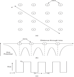
It is not easy to solve Schrödinger’s equation with these potentials. So, Kronig and Penney approximated these potentials inside the crystal to the shape of rectangular steps as shown in Fig. (c). This model is called Kronig-Penney model of potentials.

The energies of electrons can be known by solving Schrödinger’s wave equation in such a lattice. The Schrödinger time-independent wave equation for the motion of an electron along X-direction is given by:
 ...............(1)
The energies and wave functions of electrons associated with this model can be calculated by solving time-independent one-dimensional Schrödinger’s wave equations for the two regions I and II as shown in Fig.
The Schrödinger’s equations are:
 for 0<x<a.............(2)
 for -b<x<0.............(3)
We define two real quantities (say) α and β such that:

Hence, becomes:
 for 0<x<a
 for -b<x<0
According to Bloch's theorem, the wavefunction solution of the Schrödinger equation when the potential is periodic and to make sure the function u(x) is also continuous and smooth, can be written as:

Where u(x) is a periodic function which satisfies u (x + a) = u(x).
Using Bloch theorem and all the boundary conditions for the continuity of the wave function the solution of Schrodinger wave equation obtained as

Where 
This equation shows the relation between the energy (through α) and the wave-vector, k, and as you can see, since the left hand side of the equation can only range from −1 to 1 then there are some limits on the values that α (and thus, the energy) can take, that is, at some ranges of values of the energy, there is no solution according to these equation, and thus, the system will not have those energies:
Energy gaps. These are the so-called band-gaps, which can be shown to exist in any shape of periodic potential (not just delta or square barriers).
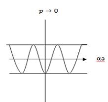
1. The permissible limit of the term

Lies between +1 to -1. By varying αa, a wave mechanical nature could be plotted as shown in Fig, the shaded portion of the wave shows the bands of allowed energy with the forbidden region as unshaded portion.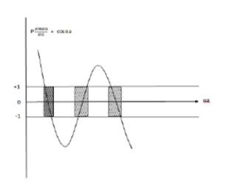
2. With increase of αa, the allowed energy states for a electron increases there by increasing the band width of the bands, i.e., the strength of the potential barrier diminishes. This also leads to increase of the distance between electrons and the total energy possessed by the individual electron.
3.Conversly if suppose the effect of potential barrier dominate i.e., if P is large, the resultant wave obtained in terms of  shows a stepper variation in the region lies between +1 to -1. This results in the decrease of allowed energy and increase of forbidden energy gap. Thus, at extremities,
Case (i) when  , the allowed energy states are compressed to a line spectrum.
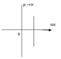
Case (ii) when  the energy band is broadened and it is quasi continuous.
An E-k diagram shows characteristics of a particular semiconductor material. It shows the relationship between the energy and momentum of available quantum mechanical states for electrons in the material.
First, consider a basic E-k band diagram like this one (the x-axis can be either momentum, pp, or wavenumber, kk, since p=ℏkp=ℏk):
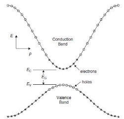
In this diagram you can see a few things:
- The band gap (EG), which is the difference in energy between the top of the valence band and the bottom of the conduction band.
- The effective mass of electrons and holes in the material. This is given by the curvature of each of the bands.
- This diagram indicates (diagrammatically) how the actual electron states are equally spaced in k-space. Which means that the density of states in E (ρ(E)ρ(E)) depends on the slope of the E-k curve.
There is a more complex form of E-k diagram that shows the relationship for different directions of k relative to the crystal lattice:
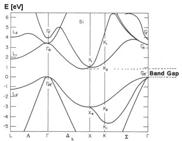
Here, the greek letters (ΓΓ, ΔΔ, K, etc.) on the x-axis indicate different directions of k relative to the crystal axes.
In addition to showing the effective mass at different band extrema, this also shows that the effective mass varies depending on the direction of conduction relative to the crystal orientation.
This type diagram also shows whether the material is a direct-gap or indirect-gap semiconductor. Direct gap is when the valence band maximum and conduction band minimum occur at the same location in k-space. This is important in optoelectronics because only direct gap materials (like GaAs, but not including silicon) have efficient radiative absorption and emission, which is what makes LEDs and laser diodes work.
Electrical conduction is the movement of electrically charged particles through a conductor or semiconductor, which constitutes an electric current. The charge transport may result as a response to an electric field (E) or by diffusion. The current density (j) is then:
j = σ E + qD∇n
With σ conductivity, q the elementary charge, D diffusion constant, and n the carrier density.
F = dP/dt = mdv/dt = ħdk/dt = q(E + v x B)
Drude Model (free electron gas model) Paul Drude in 1900 explained the transport properties of electrons in metals. The model, which is an application of kinetic theory, assumes that the microscopic behaviour of electrons in a solid may be treated classically and looks much like a pinball machine, with a sea of constantly jittering electrons bouncing and re-bouncing off heavier, relatively immobile positive ions.
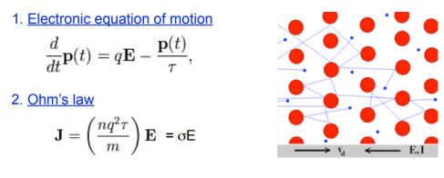
An exactly periodic lattice of positive ion cores does NOT cause scattering.
Electrons are scattered by:
1) Deviations from strict periodicity in the lattice:
a) Defects in the lattice (such as vacancies, dislocations, impurities, etc): usually fixed in space and time and temperature insensitive.
b) Lattice vibrations: varying in time and depending strongly on temperature.
2) Electron-electron collisions:
Normally this term is insignificant comparing with the above factor at room temperature and below.
ħdk/dt = -eE
If there is no scattering, electrons are moving under a constant E field,
Then
ħk(t) = mv(t) = -eEt, assume E(0) = 0
If the collision time is τ, then
v(τ) = -eEτ/m j = nqv = ne2Eτ/m = σ E
Electrical conductivity
σ = ne2τ/m
The collision time τ can, to a good approximation, be independently attributed to two factors, the phonons (τph) and impurities (τi ), and
1/τ = 1/τph + 1/τI
The collision time τ is thus a function of temperature T. For example, for copper (Cu)
τ∼ 2 x 10⁻⁹ s at 4K and τ∼ 2 x 10-14 s at 300K,
Velocity of Fermi electrons ≡ vF ~ 1.5 x 108 cm/s
Then, the mean free path (l) of conduction electrons is
l ∼ 3 mm at 4K and l ∼ 30 nm at 300K
Postulates of free electron Model
1. The outermost electrons of the constituent atom of the metal are weakly bound with the atoms. Hence these electrons get separated from their atoms and move freely inside the substance and are called free electrons.
2. There are large number of free electrons inside the metals and hey behave like molecules of a gas enclosed in a container. Hence it is called free electron gas. These free electrons are responsible for the thermal and electrical conduction inside the metal. Hence, they are also called conduction electrons.
3.The free electrons in thermal equilibrium obey Maxwell-Boltzmann statistics. Which states that the free energy per electron at an absolute temperature T is 1/2 KT, where K is Boltzmann's constant.
4. Inside the metal, free electrons move randomly with high velocity and it depends on the temperature of the metal. During the motion, their velocity and direction changes in such a way that the rate of flow of electron in a particular direction is zero.
5. When the metal is kept in external electric field, the free electrons gets attracted in the direction opposite to the direction to the external electric field. They start moving with a constant average velocity called drift velocity.
The (electrical) conductivity of a material represents how easily charges will flow through the material. Materials with high conductivity are called conductors. Materials that do not readily conduct electricity are called insulators. From these definitions, one might deduce that semiconductors form a third category of material with conductivities somewhere between conductors and insulators, but that is not exactly the case. Semiconductors, despite the name, form a subgroup of insulators and have properties that differ greatly from the properties of conductors. Pure crystalline silicon, in fact, is a rather poor conductor.
To understand how the term semiconductor arose, we return to the concepts of electron states and energy bands.
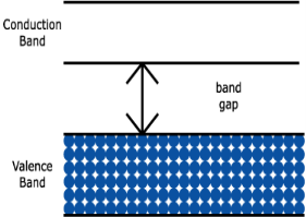
Electric current is generally due to the motion of valence electrons. An electron can move through a material only by moving from one allowed energy state to another. But most materials are formed by bonds that completely fill a valence band, as shown in figure (a) below. Electrons in this filled valence band have no empty states to move into, unless they somehow gain enough energy to jump across the forbidden band gap into the empty conduction band above. Conduction is therefore very difficult. As you might imagine, this energy band diagram represents an insulator. | ||||||
 |
|  | ||||
|
|
| ||||
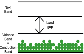
Other materials are formed by bonds that only partially fill a valence band, as shown in figure (b) above. Electrons in this partially filled valence band have plenty of empty states available, so they can move freely from the vicinity of one atom to another. A partially-filled valence band is also called the conduction band, since electrons in that band can be responsible for conduction. Not surprisingly, materials with partially-filled valence bands are conductors.
The flow of electric current due to the motion of charge carriers under the
Influence of external electric field is called drift current.
When an electric field E is applied across a semiconductor material, the charge
Carriers attain a drift velocity vd.
So, drift velocity
Vd=µE----------------(1)
The relation between current density J and drift velocity vd is
J=Nqvd
Where N is the carrier concentration
q is the charge of electron or hole
From equations (1) and (2), we get

_ is the mobility of charge carrier.
The above equation shows the general expression for drift current density.
Drift current density due to electrons is

Where is the electrons carrier concentration and
µe the mobility of electrons
Drift current density due to holes is

Total drift current density:

Origin of energy bands formation in solids
An isolated atom possesses discrete energies of different electrons. Suppose two isolated atoms are brought to very close proximity, then the electrons in the orbits of two atoms interact with each other. So, that in the combined system, the energies of electrons will not be in the same level but changes and the energies will be slightly lower and larger than the original value. So, at the place of each energy level, a closely spaced two energy levels exists. If ‘N’ number of atoms are brought together to form a solid and if these atoms’ electrons interact and give ‘N’ number of closely spaced energy levels in the place of discrete energy levels, it is known as bands of allowed energies. Between the bands of allowed energies, there are empty energy regions, called forbidden band of energies. Kronig-Penney model supports the existence of these bands of energies (allowed bands and forbidden bands). The mathematical solution for Schrödinger’s wave equation is very tedious but it provides a clue in understanding the origin of energy bands.
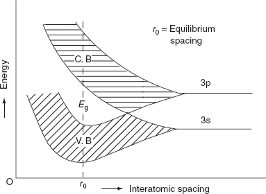
The formation of energy bands has been explained taking Sodium (Na) metal as an example. When isolated sodium atoms are brought together to form a solid, then the energy levels of the valence electrons spread into bands. The 3S and 3P orbitals electrons energies are. These bands are seen to overlap strongly at the interatomic spacing of sodium.
Figure Spreading of energy levels into energy bands in sodium metal
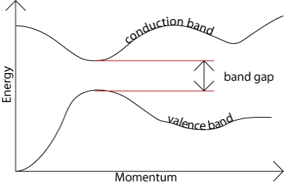
The band gap represents the minimum energy difference between the top of the valence band and the bottom of the conduction band. However, the top of the valence band and the bottom of the conduction band are not generally at the same value of the electron momentum. In a direct band gap semiconductor, the top of the valence band and the bottom of the conduction band occur at the same value of momentum, as in the schematic below.
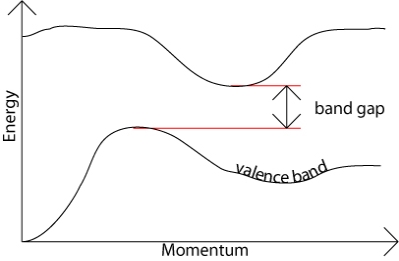
In an indirect band gap semiconductor, the maximum energy of the valence band occurs at a different value of momentum to the minimum in the conduction band energy:
The difference between the two is most important in optical devices. As has been mentioned in the section charge carriers in semiconductors, a photon can provide the energy to produce an electron-hole pair.
Each photon of energy E has momentum p = E / c, where c is the velocity of light.
An optical photon has an energy of the order of 10–19 J, and, since c = 3 × 10⁸ ms–1, a typical photon has a very small amount of momentum.
A photon of energy Eg, where Eg is the band gap energy, can produce an electron-hole pair in a direct band gap semiconductor quite easily, because the electron does not need to be given very much momentum. However, an electron must also undergo a significant change in its momentum for a photon of energy Eg to produce an electron-hole pair in an indirect band gap semiconductor. This is possible, but it requires such an electron to interact not only with the photon to gain energy, but also with a lattice vibration called a phonon in order to either gain or lose momentum.
The same principle applies to recombination of electrons and holes to produce photons. The recombination process is much more efficient for a direct band gap semiconductor than for an indirect band gap semiconductor, where the process must be mediated by a phonon.
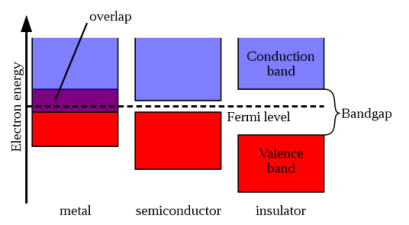
According to band theory, the electrons in a solid can possess bands of energies called allowed bands of energies and these electrons may not possess some other bands of energies called forbidden bands of energies. The allowed bands of energies and forbidden bands of energies are present alternatively one after another for the electrons of a solid. The top-most band is called Conduction band and the next band below Conduction band is valance band. These two bands are separated by forbidden band.
1. Insulator: The valence band of those materials remains full of electrons. The conduction band of those materials remains empty. The forbidden energy gap between the conduction band and the valence band is widest. The difference is more than 4 eV. Crossing the forbidden energy gap from valence band to conduction band require large amount of energy. Mica, glass, ebonite etc are the examples of insulators.
2. Metal: The valence band and the conduction band overlap each other. There is no forbidden energy gap here so Eg=0. At absolute zero temperature large number of electrons remains in the conduction band. The resistance of conductor is very low; large number charge carriers are available here. So, the electricity can pass easily through the conductors. Aluminium, Silver, etc are good conductors
3. Semiconductors: A semiconductor remains partially full valence band and partially full conduction band at the room temperature the energy gap is narrower. The conduction band remains full empty of a semiconductor where the valence band remains full of electrons at absolute zero temperature. The value of Eg =1.1eV for silicon crystal and Eg=0.7eV for germanium. It can easily overcome due to thermal agitation or light. So, silicon and germanium are insulators at absolute zero temperature. On the other hand, with the increasing of temperature the electrical conductivity of semiconductors increases.
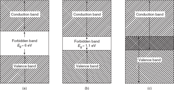
(a) Band diagram of Insulator (diamond); (b) Band diagram of Semiconductor (silicon); (c) Band diagram of a metal
As discussed in “Band Gaps”, the valence and conduction bands represent groups of energy states of the electrons. However, according to something called the Pauli exclusion principle, a result of quantum mechanics, each allowed energy level can be occupied by no more than two electrons of opposite “spin”. This just means that, at low temperatures, all available states in the crystal up to a certain energy level will be occupied by two electrons
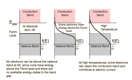

Where T is temperature, k is Boltzmann’s constant (1.38 x 10⁻²³ Joules per Kelvin), EF is the Fermi energy level of a given material and E is the allowed energy state whose probability we are trying to find. This equation just means that as temperature increases, electrons are more likely to be found in the higher energy states. When the temperature is near absolute zero, we see that f(E) becomes 1, giving that nearly all the electrons are below the Fermi level at higher temperatures, energy levels in the conduction band have a higher probability of occupation and levels in the valence band are more likely to be empty. There is also an equation which allows us to solve for the Fermi level of a material using our knowledge of the band gap of that material.
The highest energy level that an electron can occupy at the absolute zero temperature is known as the Fermi Level. The Fermi level lies between the valence band and conduction band because at absolute zero temperature the electrons are all in the lowest energy state.
In a p type semiconductor, there is an increase in the Density of unfilled States. Thus, more electrons can be accommodated at lower energy states. In a n type semiconductor, the DOS is increased. Thus, electrons have to be accommodated at higher energy levels.
Fermi level is also defined as the work done to add an electron to the system. More positive (more holes) in a p type semiconductor, mean lesser work needs to be done. Hence a lower Fermi level.
Some points about Fermi levels:
- They allow us to make calculations as to the density of electrons and holes in a material, or the relative amounts of each, depending on the temperature. This is crucial to our understanding of current flow through semiconductors.
- In conductors (i.e. metals), electrons only partially fill the valence band and the valence and conduction bands are very close or overlap, thus electrons become conductive (free) very easily. On the other hand, insulators and semiconductors have Fermi levels lying in the forbidden band gap and have full valence bands, therefore insulators have electrons with nowhere to go (hence non-conductive) and semiconductors become conductive only at certain temperatures (when more electrons can be found in the higher energy states due to thermal excitation).
- The Fermi level and band gap in a solid largely determine its electrical properties. In a perfect semiconductor (in the absence of impurities/dopants), the Fermi level lies close to the middle of the band gap.
The mass of an electron in the periodic potentials of a crystal is different from the free electron mass and is usually referred to as the effective mass. According to de Broglie hypothesis, a moving electron is associated with a wave. The velocity of an electron (v) is equal to the group velocity (vg) of the associated wave. The group velocity is given by:
 ...................(1)
Where ω is the angular frequency (2πν) and K is the propagation vector of the wave.
In quantum mechanics, the energy, ‘E’ of an electron is given by:
E = ħω ...........(2)
Substituting value of w from eq (2) to eq (1), we get
 ............(3)
Differentiating Equation (3) with respect to ‘t’, we get acceleration of electron as

 .............(4)
In quantum theory, the momentum of an electron is given by:
 ...........(5)
Differentiating momentum with respect to t
 ................(6)
Eq no (4) using eq no (6), reduces to
 .....................(7)
Using Newtons second law  equation (6) reduces to

 ...........(8)
This mass of an electron is called the effective mass of an electron, denoted as m*.
The effective mass is thus determined by d2E/dK2.
From band theory of solids, we know E is not proportional to K2.

The variation of E with K is shown in Fig. Using the type of variation of E with K
Plot v versus K as shown in Fig. (b). At the bottom of the energy band, the velocity of an electron is zero and as the value of K increases, the velocity increases and attains a maximum value at K = K0, known as the point of inflection on the E−K curve. Beyond this point, the velocity decreases and attains zero at  , which is the top of the band. The negative values of the wave vector exhibit a similar behaviour. Thus, a feature, which is altogether different from the behaviour of free electrons, is observed.
The effective mass is represented as a function of K in Fig.(c). For the lower portion of E-K curve, d2E/dK2is positive so m* is positive, and increases with increase of K, attains a maximum value at the point of inflectionK0. For further higher values of K,  is negative, hence m* is negative. As
  , the effective mass approaches to a smaller negative value. At the point of inflection [(d2E/dK2) = 0], m* becomes infinite.
Physically, that in the upper half of the band, the electron behaves as having negative mass or as behaving like particles with positive charges. Suppose an electron starts at K = 0, when an electric field is applied, the wave vector increases linearly with time. Until the velocity reaches its maximum value, the electron is accelerated by the field, beyond this maximum velocity the same field produces a decrease in velocity, i.e., the mass must become negative in the upper part of the band.
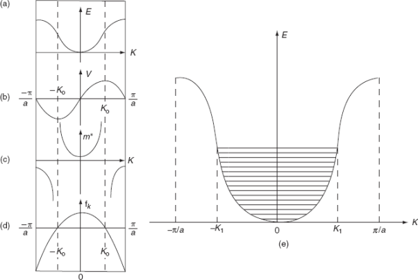
(a) E-K diagram; (b) Velocity versus K; (c) Effective mass of an electron; (d) Degree of freedom of an electron; (e) E-K diagram
The density of states in a semiconductor equals to the number of states per unit energy and per unit volume.
Calculation of Density of states
We will assume that the semiconductor can be modelled as an infinite quantum well in which electrons with effective mass, m*, are free to move. The energy in the well is set to zero. The semiconductor is assumed a cube with side L.
This assumption does not affect the result since the density of states per unit volume should not depend on the actual size or shape of the semiconductor.
Consider a sphere in k-space. Associated with this sphere volume will be

Where k is our “radius" where

We now define a state by the smallest nonzero volume it possesses in k-space. This occurs when

A cube in k-space with size L (Lx = Ly = Lz =L) as indicated on Figure


Thus, within our imagined spherical volume of k-space, the total number of states present is


Next, when dealing with electrons and holes, we must consider spin degeneracy, since two carriers, possessing opposite spin, can occupy the same state. As a consequence, we multiply the above expression by 2 to obtain

Density of states is number of states per unit volume per unit energy range, therefore dividing N with volume (L3) and differentiating it with respect to E

Or

As 

Or 

Or
This is our desired density-of-states expression for a bulk three dimensional solid.
Energy band dia:
Atoms have been seen to have discrete energy levels. When a huge number of atoms are combined to form a solid however, these discrete energy levels are replaced by discrete ranges of energy, or energy bands, within which there are so many individuals allowed energy values that within the bands the distribution can be considered to be continuous. This idea is seen in the following figure:
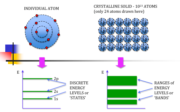
In between energy bands are ranges of energy which are entirely impossible known as band gaps.
Different substances have different band structures which in many ways dictate the characteristics of that substance in terms of electrical conduction, as there exists an energy band called the conduction band, in which electrons can be propagated as current. The valence band on the other hand is the energy level of valence electrons which are bound into the atomic structure of the substance.
When a substance is placed in an electric field its electrons gain potential energy. For a metal (conductor) the conduction and valence bands overlap, and so the additional energy is enough to free electrons and cause current as there are allowable energy values directly above the initial state. For insulators however, there is often a band gap between the initial energy state and the next possible value, and so a huge amount of energy is required to cause the electron to be freed and accelerated as current. For semiconductors there is still a band gap however it is a lot smaller. This is all seen in the following band diagram:
