Unit – 9
Semiconductors
Contents:
Intrinsic semiconductor
Pure semiconductors are called intrinsic semiconductors.
Silicon and germanium are the most common examples of intrinsic semiconductors. Both these semiconductors are most frequently used in the manufacturing of transistors, diodes and other electronic components.
Intrinsic semiconductor is also called as undoped semiconductor or I-type semiconductor. In intrinsic semiconductor the number of electrons in the conduction band is equal to the number of holes in the valence band. Therefore, the overall electric charge of atom is neutral.
The semiconductor in which impurities are added is called extrinsic semiconductor. When the impurities are added to the intrinsic semiconductor, it becomes an extrinsic semiconductor. The process of adding impurities to the semiconductor is called doping. Doping increases the electrical conductivity of semiconductor.
Extrinsic semiconductor
Extrinsic semiconductor has high electrical conductivity than intrinsic semiconductor. Hence the extrinsic semiconductors are used for the manufacturing of electronic devices such as diodes, transistors etc. The number of free electrons and holes in extrinsic semiconductor are not equal.
Types of impurities
Two types of impurities are added to the semiconductor. They are pentavalent and trivalent impurities.
Pentavalent impurities
Pentavalent impurity atoms have 5 valence electrons. The various examples of pentavalent impurity atoms include Phosphorus (P), Arsenic (As), Antimony (Sb), etc. The atomic structure of pentavalent atom (phosphorus) and trivalent atom (boron) is shown in below fig.
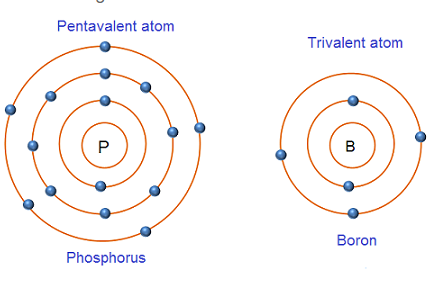
Phosphorus is a substance consisting of atoms which all have the same number of protons. The atomic number of phosphorus is 15 i.e. 15 protons. The number of protons in the nucleus of an atom is called atomic number. Phosphorus atom has 15 electrons (2 electrons in first orbit, 8 electrons in second orbit and 5 electrons in the outermost orbit).
Trivalent impurities
Trivalent impurity atoms have 3 valence electrons. The various examples of trivalent impurities include Boron (B), Gallium (G), Indium (In), Aluminium (Al).
Boron is a substance consisting of atoms which all have the same number of protons. The atomic number of boron is 5 i.e. 5 protons. Boron atom has 5 electrons (2 electrons in first orbit and 3 electrons in the outermost orbit).
Classification of extrinsic semiconductors based on impurities added
Based on the type of impurities added, extrinsic semiconductors are classified in to two types.
N-type semiconductor
P-type semiconductor
Negative charge carriers (Electron)
The negative charge carriers such as free electrons are the charge carriers that carry negative charge with them while moving from one place to another place. Free electrons are the electrons that are detached from the parent atom and moves freely from one place to another place.
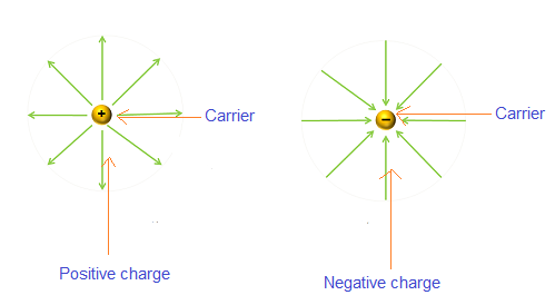
Positive charge carriers (Holes)
The positive charge carriers such as holes are the charge carriers that carry positive charge with them while moving from one place to another place. Holes are the vacancies in valence band that moves from one place to another place within the valence band.
The charge carriers that are present in large quantity are called majority charge carriers. The majority charge carriers carry most of the electric charge or electric current in the semiconductor. Hence, majority charge carriers are mainly responsible for electric current flow in the semiconductor.
The charge carriers that are present in small quantity are called minority charge carriers. The minority charge carriers carry very small amount of electric charge or electric current in the semiconductor.
Charge carriers in intrinsic semiconductor
The semiconductors that are in pure form are called intrinsic semiconductors. In intrinsic semiconductor the total number of negative charge carriers (free electrons) is equal to the total number of positive charge carriers (holes or vacancy).
Total negative charge carriers = Total positive charge carriers
The highest energy level that an electron can occupy at the absolute zero temperature is known as the Fermi Level. The Fermi level lies between the valence band and conduction band because at absolute zero temperature the electrons are all in the lowest energy state.
In a p type semiconductor, there is an increase in the Density of unfilled States. Thus, more electrons can be accommodated at lower energy states. In an n type semiconductor, the DOS is increased. Thus, electrons have to be accommodated at higher energy levels.
Fermi level is also defined as the work done to add an electron to the system. More positive (more holes) in a p type semiconductor, mean lesser work needs to be done. Hence a lower Fermi level
When the material is at a temperature higher than OK, it receives thermal energy from surroundings i.e. electrons are thermally excited. As a result, they move into the higher energy levels which are unoccupied at OK. The occupation obeys a statistical distribution called Fermi – Dirac distribution law.
According to this distribution law, the probability F(E) that a given energy state E is occupied at a temperature T is given by

Here F(E) is called Fermi – Dirac probability function. It indicates that the fraction of all energy state (E) occupied under thermal equilibrium ‘K’ is Boltzmann constant.
Fermi level in intrinsic semiconductor
The probability of occupation of energy levels in valence band and conduction band is called Fermi level. At absolute zero temperature intrinsic semiconductor acts as perfect insulator. However as the temperature increases free electrons and holes gets generated.
In intrinsic or pure semiconductor, the number of holes in valence band is equal to the number of electrons in the conduction band. Hence, the probability of occupation of energy levels in conduction band and valence band are equal.
Therefore, the Fermi level for the intrinsic semiconductor lies in the middle of forbidden band.
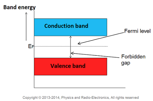
Fermi level in the middle of forbidden band indicates equal concentration of free electrons and holes.
The hole-concentration in the valence band is given as

The electron-concentration in the conduction band is given as

Where KB is the Boltzmann constant
T is the absolute temperature of the intrinsic semiconductor
Nc is the effective density of states in the conduction band.
Nv is the effective density of states in the valence band.
The number of electrons in the conduction band is depends on effective density of states in the conduction band and the distance of Fermi level from the conduction band.
The number of holes in the valence band is depends on effective density of states in the valence band and the distance of Fermi level from the valence band.
For an intrinsic semiconductor, the electron-carrier concentration is equal to the hole-carrier concentration.
It can be written as
p = n = ni
Where P = hole-carrier concentration
n = electron-carrier concentration
And ni = intrinsic carrier concentration
The fermi level for intrinsic semiconductor is given as,

Where EF is the fermi level
EC is the conduction band
EV is the valence band
Therefore, the Fermi level in an intrinsic semiconductor lies in the middle of the forbidden gap
Fermi level in extrinsic semiconductor
In extrinsic semiconductor, the number of electrons in the conduction band and the number of holes in the valence band are not equal. Hence, the probability of occupation of energy levels in conduction band and valence band are not equal. Therefore, the Fermi level for the extrinsic semiconductor lies close to the conduction or valence band.
Fermi level in n-type semiconductor
In n-type semiconductor pentavalent impurity is added. Each pentavalent impurity donates a free electron. The addition of pentavalent impurity creates large number of free electrons in the conduction band.
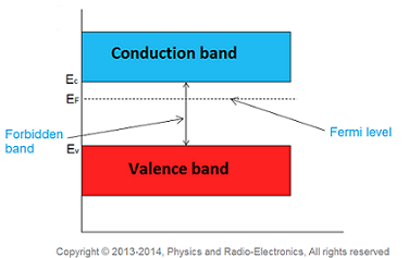
At room temperature, the number of electrons in the conduction band is greater than the number of holes in the valence band. Hence, the probability of occupation of energy levels by the electrons in the conduction band is greater than the probability of occupation of energy levels by the holes in the valence band. This probability of occupation of energy levels is represented in terms of Fermi level. Therefore, the Fermi level in the n-type semiconductor lies close to the conduction band.
The Fermi level for n-type semiconductor is given as

Where, EF is the Fermi level.
EC is the conduction band.
KB is the Boltzmann constant.
T is the absolute temperature.
NC is the effective density of states in the conduction band.
ND is the concentration of donor atoms.
Fermi level in p-type semiconductor
In p-type semiconductor trivalent impurity is added. Each trivalent impurity creates a hole in the valence band and ready to accept an electron. The addition of trivalent impurity creates large number of holes in the valence band.
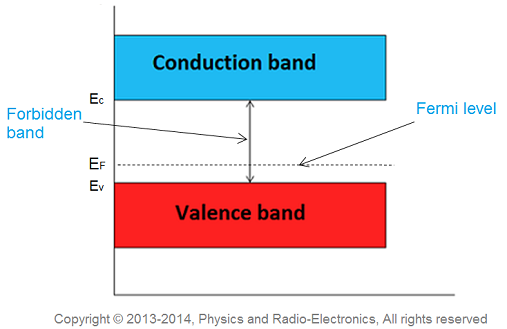
At room temperature, the number of holes in the valence band is greater than the number of electrons in the conduction band. Hence, the probability of occupation of energy levels by the holes in the valence band is greater than the probability of occupation of energy levels by the electrons in the conduction band. This probability of occupation of energy levels is represented in terms of Fermi level. Therefore, the Fermi level in the p-type semiconductor lies close to the valence band.
The Fermi level for p-type semiconductor is given as

Where NV is the effective density of states in the valence band.
NA is the concentration of acceptor atoms.
When we are trying to determine the position of the Fermi level, we assume the semiconductor is in equilibrium. EF on the band diagram is a function of temperature and carrier concentration. This can be seen from the equations used to determine the position of the Fermi level.
Intrinsic semiconductor |  |
n-type semiconductor |  |
p-type semiconductor |  |
If the temperature is varied, the Fermi level will also vary.
The conductivity of an intrinsic semiconductor can be increased by adding small amounts of impurity atoms, such as III rd or Vth group atoms. The conductivity of silica is increased by 1000 times on adding 10 parts of boron per million part of silicon. The process of adding impurities is called doping and the impurity added is called dopant.
The basic theoretical methods for treating defects and, in particular, impurities in semiconductors are first reviewed. They split into two groups: the techniques appropriate to deep states (local density, empirical tight binding) or to shallow states (effective mass approximation). A discussion is given of how to handle the most difficult intermediate cases (corresponding to the shallow-deep instability) and of the possible coexistence of these two types of states.
The second part describes applications of these general arguments to specific cases. This begins with the well documented case of transition metal impurities followed by recent results obtained for rare earth impurities. A fairly detailed analysis is performed in the case of EL2 showing that this centre must be a complex involving the antisite. The case of the DX donor in Ga1-xAlxAs compounds is also reviewed, with the arguments in favour of the two competing models.
N – Type semiconductor
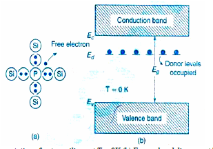
In a pure (intrinsic) semiconductor, when pentavalent an impurity like Phosphorous atom consisting of five valance electrons is doped, and then concentration of electrons increases than holes. Hence the given semiconductor formed is called N – type semiconductor. This is shown in the figure 7a below. By adding donor impurities, the free electrons generated or donated, form an energy level called as “Donor energy level” i.e. ED is shown in the figure below.
P- type semiconductor
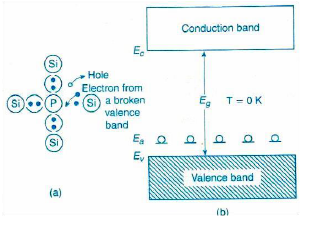
P – Type semiconductor is formed by doping with trivalent impurity atoms (acceptor) like III rd group atoms i.e. Aluminium, Gallium, and Indium etc to a pure semiconductor like Ge or Si. As the acceptor trivalent atoms has only three valance electrons & Germanium, Silicon has four valence electrons; holes or vacancy is created for each acceptor dopant atom. Hence holes are majority and electrons are minority. It is shown in the figure a below. Also, an acceptor energy level „EA‟ is formed near VB consisting of holes, as shown in the figure below:
The process by which free electrons and holes are generated in pair is called generation of carriers.
When electrons in a valence band get enough energy, then they will absorb this energy and jumps into the conduction band. The electron which is jumped into a conduction band is called free electron and the place from where electron left is called hole. Likewise, two type of charge carriers (free electrons and holes) gets generated.
Recombination of carriers (free electrons and holes)
The process by which free electrons and the holes get eliminated is called recombination of carriers. When free electron in the conduction band falls in to a hole in the valence band, then the free electron and hole gets eliminated.
The law of mass action states that the product of number of electrons in the conduction band and the number of holes in the valence band is constant at a fixed temperature and is independent of amount of donor and acceptor impurity added.
Mathematically it is represented as
Np = ni2 = constant
Where ni is the intrinsic carrier concentration
n is number of electrons in conduction band
p is number of holes in valence band
Law of mass action for extrinsic semiconductor
The law of mass action is applied for both intrinsic and extrinsic semiconductors. For extrinsic semiconductor the law of mass action states that the product of majority carriers and minority carriers is constant at fixed temperature and is independent of amount of donor and acceptor impurity added.
Law of mass action for n-type semiconductor
The law of mass action for n-type semiconductor is mathematically written as
nn pn = ni2 = constant
Where nn= number of electrons in n-type semiconductor
pn = number of holes in n-type semiconductor
The electrons are the majority carriers and holes are the minority carriers in n-type semiconductor.
In n-type semiconductor, as the number of electrons (majority) in the conduction band increases the number of holes (minority) in the valence band decreases.
Therefore, the product of electrons (majority) and holes (minority) remains constant at fixed temperature.
Law of mass action for p-type semiconductor
The law of mass action for p-type semiconductor is mathematically written as
pp np = ni2 = constant
Where pp = number of holes in p-type semiconductor
np = number of electrons in p-type semiconductor
The holes are the majority carriers and electrons are the minority carriers in p-type semiconductor.
In p-type semiconductor, as the number of holes (majority) in the valence band increases the number of electrons in the conduction band (minority) decreases. Therefore, the product of holes (majority) and electrons (minority) remains constant at fixed temperature.
Charge neutrality occurs when all the charge in a volume adds to zero; it is neutral, neither positive nor negative. The equation for charge density (Coulombs/cm3) is:
r = q(whatever has charge)
Where q = electronic charge.
In a semiconductor, the most common and most prominent sources of charge are electrons holes, and ionized acceptors and ionized donors.
The zero net charge does not mean that the electrons, holes, ionized donors, and ionized acceptors are not present in the semiconductor. It simply states that in a uniformly doped semiconductor the negative charge associated with an electron or ionized acceptor would be cancelled by the positive charge associated with a hole or ionized donor. This does not mean that the actual electrons, holes, and ionized impurities have ceased to exist in the semiconductor, it means that r = 0.
If r = q(po - no + ND - NA) = 0, then the sum of the charges associated with the carriers must equal zero:
po - no + ND - NA = 0 |
This equation is useful in many areas, including computing po and no in equilibrium. We usually consider NA and ND to be known, so it gives us one equation to relate two unknowns, po and no. We also know that pono=ni2 and ni is considered known, so we can use the two equations to solve for po and no in terms of ND, NA, and ni.
In case of semiconductors we observe two kinds of currents
- Drift current
- Diffusion current
Drift current
The flow of electric current due to the motion of charge carriers under the
Influence of external electric field is called drift current.
When an electric field E is applied across a semiconductor material, the charge
Carriers attain a drift velocity vd.
So, drift velocity
Vd=µE----------------(1)
The relation between current density J and drift velocity vd is
J=Nqvd
Where N is the carrier concentration
q is the charge of electron or hole
From equations (1) and (2), we get

_ is the mobility of charge carrier.
The above equation shows the general expression for drift current density.
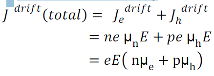
Drift current density due to electrons is

Where is the electrons carrier concentration and
µe the mobility of electrons
Drift current density due to holes is

T Total drift current density:
Diffusion current:
The flow of electric current due to the motion of charge carriers under concentration gradient is called diffusion current.
Or
The motion of charge carriers from the region of higher concentration to lower
Concentration leads to a current called diffusion current.
Let be the excess electron concentration. Then according to Fick’s law, the rate of
Diffusion of charge carriers is proportional to concentration gradient is

Hence
Rate of diffusion of charge:
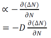
Where D is the diffusion coefficient of charge carriers
The negative sign indicates decrease of N with increase of x
So, the diffusion current density Jdiffu is:

The expression for total current density due to holes is

The expression for total current density due to electrons is

When a layer of P - type semiconducting material is placed with a layer of N- type semiconducting material in such a way that the atoms of P-type combine with the atoms of N-type across the surface of contact, such a surface junction where combination has occurred is known as PN junction.
Combined p-type and n-type semiconductors with PN junction formation is known a junction diode or PN diode
Biased p-n junction diode by diffusion technique:
Diffused junctions are formed by impurity diffusion technique. The diffusion process employs either gas diffusion method or solid diffusion method for example in gas diffusion method a wafer of n-type silicon is heated at about 10000 c in a gaseous atmosphere of high concentration gradient the boron atoms.
At the temperature due to concentration gradient the boron atom diffuses in to silicon forming p-n junction in solid diffusion process a p-type impurity (say indium) is painted on a n-type substrate and both are heated. Now impurity atoms diffuse into n-type substrate for a short distance and form p-n junction.

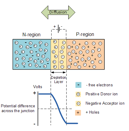
- The formation PN junction is represented in a figure. Let us consider the formation of a sharp junction when two separate semiconductors of p and n type are brought together.
- The p-type has holes as majority carriers and electrons as minority carriers while n-type has electrons as majority carries and holes as minority carriers.
- When they are joined, in the region of contact the free electrons diffuse from n-region and combine with holes in p-region. This leaves n-region near the boundary positively charged and p-region negatively as a result, electric field EB appears in a small region W on either side of the junction O. This region is called “Depletion region “. The thickness of this region is in the older of 6 ×10⁻⁶ cm.
- Due to electric field E B potential difference appears across the depletion region and this potential VB is called “Contact Potential or Barrier Potential or Junction Barrier”.
When the N-type semiconductor and P-type semiconductor materials are first joined together a very large density gradient exists between both sides of the PN junction. The result is that some of the free electrons from the donor impurity atoms begin to migrate across this newly formed junction to fill up the holes in the P-type material producing negative ions.
However, because the electrons have moved across the PN junction from the N-type silicon to the P-type silicon, they leave behind positively charged donor ions ( ND ) on the negative side and now the holes from the acceptor impurity migrate across the junction in the opposite direction into the region where there are large numbers of free electrons.
As a result, the charge density of the P-type along the junction is filled with negatively charged acceptor ions ( NA ), and the charge density of the N-type along the junction becomes positive. This charge transfer of electrons and holes across the PN junction is known as diffusion. The width of these P and N layers depends on how heavily each side is doped with acceptor density NA, and donor density ND, respectively.
This process continues back and forth until the number of electrons which have crossed the junction have a large enough electrical charge to repel or prevent any more charge carriers from crossing over the junction. Eventually a state of equilibrium (electrically neutral situation) will occur producing a “potential barrier” zone around the area of the junction as the donor atoms repel the holes and the acceptor atoms repel the electrons.
Since no free charge carriers can rest in a position where there is a potential barrier, the regions on either side of the junction now become completely depleted of any more free carriers in comparison to the N and P type materials further away from the junction. This area around the PN Junction is now called the Depletion Layer.
Energy Band Diagram of PN Diode:
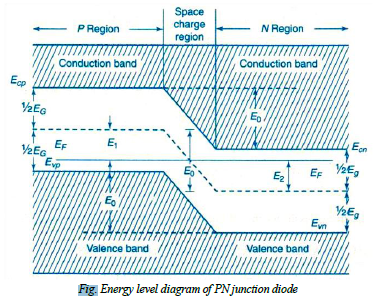
The contact potential VB across the junction is due to the potentials of depletion region on n- side denoted by Vn and p – side denoted by Vp
i.e.: VB = Vn - Vp →(7)
The energy levels of valance band, conduction band and Fermi level of both p- type and n- type semiconductors. When P-n junction is formed the Fermi, levels become common for both the types formation of potential barrier is represented in fig.
The contact potential separates the energy bands in p—type and n- type crystals. Since there is no net current flow at equilibrium i.e. under unbiased condition, it should have common Fermi level. Hence in PN junction diode the valance and conduction band energy levels Evp and Ecp of p- type and at higher level compared to the valance and conduction band energy levels Evn and Ecn of n-type. The electric field EB across the junction is given by
EB = Evp - Evn = Ecp - Ecn = e VB →(8)
Biased PN Junction:
When the PN junction is unbiased, it is in equilibrium and contact potential VB (= Vn- Vp) appears across the depletion region.
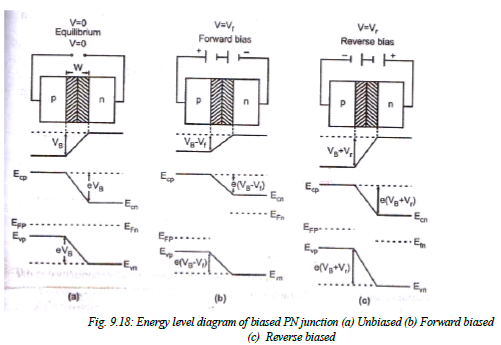
- If now an external voltage is applied across depletion region such that positive of the source is connected to the p-type side and negative of the source is connected to the n-type then junction is said to be “Forward biased”. This voltage Vf appears across the depletion region. As the contact potential difference VB acts from n top the electrostatic potential barrier is lowered and is given by VB -Vf.
- If the external voltage Vr is applied across the depletion region such that the negative of the source is connected to the p- type side and positive of source is connected to the n- type side then the junction is said to be “Reverse biased:. Since this potential act along VB, the electrostatic potential barrier increases. And is given by VB+Vr. Thus, on application of forward bias, the electric field in the transition region reduces and the application of reverse bias increases the electric field in the transition region.
- Since the width of the transition region is propositional to the square root of the electrostatic potential barrier, the width of the transition region decreases under forward bias and increases under reverse bias.
When a metal and an n-type semiconductor are joined and ΦM < ΦS, electrons will flow from the Fermi energy level in the metal into the semiconductor conduction band to lower their energy. This will cause the chemical potential of the semiconductor to move up into equilibrium with that of the metal. It will also deform the semiconductor bands, so that they curve upwards away from the metal.
This type of contact yields a linear relationship between the voltage applied and the current that flows across the junction. It is therefore called an Ohmic contact, because it obeys Ohm's law. This type of contact is also described as metallization, and is used to supply electric current into semiconductor devices.
The Schottky Diode
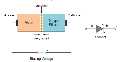
Unlike a conventional pn-junction diode which is formed from a piece of P-type material and a piece of N-type material, Schottky Diodes are constructed using a metal electrode bonded to an N-type semiconductor. Since they are constructed using a metal compound on one side of their junction and doped silicon on the other side, the Schottky diode therefore has no depletion layer and are classed as unipolar devices unlike typical pn-junction diodes which are bipolar devices.
The most common contact metal used for Schottky diode construction is “Silicide” which is a highly conductive silicon and metal compound. This silicide metal-silicon contact has a reasonably low ohmic resistance value allowing more current to flow producing a smaller forward voltage drop of around Vƒ<0.4V when conducting. Different metal compounds will produce different forward voltage drops, typically between 0.3 to 0.5 volts.
