Module 2
Semiconductor Diodes and Applications
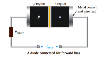
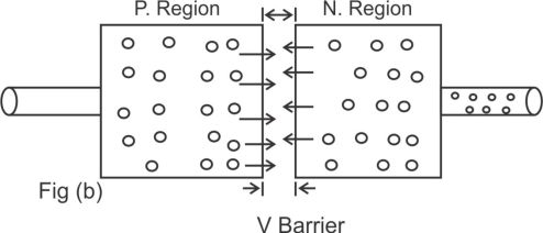
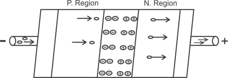
- A Forward biased showing the flow of majority carriers and the voltage due to the barrier potential across the depletion region
- To bias a diode, apply d.c. Voltage across it.
- Forward bias is the condition that allows current through the PN junction.
- Negative side of VBIAS is connected to the N -region of the diode and the positive side is connected to the P- region.
- A selected requirement is that the bias voltage VBIAS must be greater than the barrier potential.
- Because of like charges repel, the negative side of the bias voltage source pushes the free electrons, which are the majority carriers in the N-region towards the PN junction. The flow of free is called Electron Current.
- The –ve side of the source also provide a continues flow of electrons through the external connection (conductor).
- Into the N-region as show in fig-B
- The bias voltage source imparts sufficient energy to the free electrons for them to overcome the barrier potential of the depletion region and move on through into the 'p' region once in the P-region. These conduction electrons have lost enough energy to immediately combine with holes in the valence band.
- Now the e- are in the valance band in the P-region simply because they have lost too much energy overcoming the barrier potential to remain in the conduction band. Since unlike charge attract, the positive side of the bias voltage source attracts the valence electrons toward the left end of the region.
- The hole in the P-region provide the medium or "Pathway" for these valence electrons to move through the P-region.
- The holes which are the majority carriers in the P-region, effectively (not actually) move to the right toward the junction as shown in fig-B.
- The defective flow of holes is called the hole current.
- As from Fig-B hole current as the flow of valence electrons through the P-region with the holes providing the only means for these electrons to flow.
- As the electrons flow out of the P-region through the external connection and to the positive side of the bias in the P-region at the same time these electrons become conduction electrons in the mater conductor.
- To these is a continues availability of holes effectively moving towards the PN junction stream of electrons as they come across the junction in to the P-region.
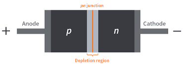
The effect of forward bias on the depletion region:

 + -
+ -


 -
-
Depletion Region
- Forward bias narrows the depletion region & produce a voltage drop across p-n junction equal to the barrier potential.
- As more electrons flow into the depletion region, the number of positive ions is reduced. As more notes effectively flow into the depletion region on the other side of the p-n junction, the number of -ve ions is reduce this reduction in positive & -ve ions during forward bias causes the depletion region to narrow.
The Effect of the Barrier Potential during forward bias:
- The electronic field between the positive and negative ions in the depletion region on either side of the junction creates an energy bill, that prevent free R form diffusing across the junction at equilibrium this is known as the barrier potential
- When forward bias is applied the free electrons are provided with enough energy from the bias voltage source to overcome the barrier potential and effectively climb the energy bill and cross the depletion region.
- The energy that the electronics repair in order to pass through the depletion region is equal to the barrier potential.
- Electron gives up an amount of energy equivalent to the barrier potential when they cross the depletion region.
- This energy loss results in a voltage drop across the p-n junction equals to the barrier potential (0.7v)
- An additional small voltage drops across the P & N regions due to the internal resistance of the material.
- For doped Semiconductor material, this resistance called the dynamic resistance is very small and can usually be neglected.
REVERSE BIAS:
Reverse bias is the condition the essentially prevents current through the diode.


P-region N- region


- +
V BIAS
A Diode connected for Reverse Biased-
- Because unlike charges attract the positive side of the bias voltage source pulls the free election, which are the majority carriers in the N-region away from the PN junction.
- AS the election flow towards the positive side of the voltage source additional positive ions are created
- This results in a widening of the depletion region and a depletion of majority carriers.


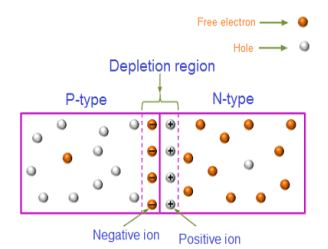
- The diode during the short transition time immediately after reverse bias voltage is applied
- In the P-region electrons from the negative side of the voltage source enter as valence electron and move from hole to hole toward the depletion region where the creators additional -ve ions.
- This results in a widening of the depletion region and a depletion of majority carriers
- As the depletion region widens the availability of majority carriers decreases
- As more of the N & P regions become depleted of majority carriers, the electric field between the positive and -ve ions increase in strength the depletion region equals the bias voltage. This point the transition current essentially ceases except for a small reverse current that can usually be neglected.
Reverse Current
- Extremely small current that exist in reverse bias after the transition current dies act is caused by the minority carrier in the N& P region that are produced by the manly generated e hole pairs.
- The conduction band in the P-region is at a higher energy level then the conduction band in the N-region. Therefore, the minority easily pass through the depletion region because they required no additional energy.
The Extremely small reverse current in a reverse biased diode is due to the minority carriers from thermally generated
e=hole pairs
The Diode - Before doping the p-type & N-type consisting silicon material atom acting as a neutral.
IF a piece of intrinsic silicon is doped so that part is n-type and the other part is p-type, a junction forms at the bounded between the two regions and a diode is created.
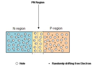
Formation of the Depletion Region
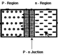
At the instant of junction formation, free electrons in the N-region near the p-n junction being to diffuse across the junction and fall into holes near the junction in the P-region.
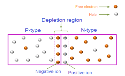
For every electron that defuse across the junction and combines with a hole, a positive charge is left in the region and a ve charge is created in the p-region firming a barriers potential. This action continues until the voltage of the barrier ripples further diffusion.
The Depletion region acts as a barrier to the farther movement of electrons across the junction
As positive ion & -ve ion across the junction produces a electric field across the junction -according to coulombs law.
The potential difference of the electric field across the depletion region is the amount of voltage required to move electronics through the electric field, this potential difference is called the barrier potential & is expressed in volt.
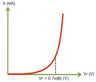
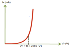
The typical barrier potential is approximately 0.7 v for silicon & 0.3 v for germanium at 25c.
When the diode is forward biased the thickness of depletion region reduces (VD>0) and the diode acts like a short circuit. There is large amount of current flowing due to this short circuit.
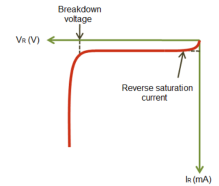
When the diode is reverse biased the thickness of depletion region increases (VD<0) and the diode acts as an open circuit. There is high voltage and no current dure to open circuit.
The diode current equation is given as
I=I0 ( – 1)
– 1)
I = diode current
I0 = Saturation current
Q=charge
V=Voltage applied across diode
K= Boltzmann constant=1.38x10⁻²³ JK-1
T= temperature in kelvin
For forward biased diode large amount of current flows so the above equation becomes
I=I0 ( )
)
As the current is large so 1 is neglected.
For reverse biased diode the exponential term is neglected so the current equation becomes
I=I0
In this we approximate the non-linear behaviour of the diode so that is eases the circuit analysis. Below shown are the condition for approximation.
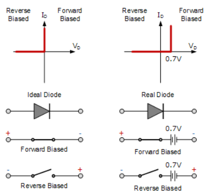
When diode is forward biased and acts a perfect conductor allowing zero potential drop is called an ideal diode. For reverse bias it acts as complete insulator.
Another approximation is when the diode id considered forward biased and connected to a battery in series. For Si diode 0.7V is required to make the diode forward biased.
For forward bias VF=VO+IFRF
For Si diode
VF=0.7+IFRF
The third approximation is when the diode has voltage across it and bulk resistance RB is also connected across the diode.
The resistance will change according to the flow of current and the forward voltage through diode for any given time.
Vd = 0.7+IdRB
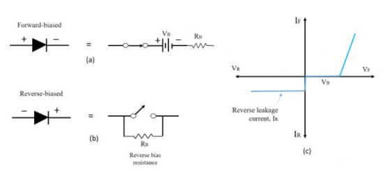
The relation for current and voltage can be expressed here as
VS = IDR +VD
ID = (VS-VD)/R
Finding load line through the example below
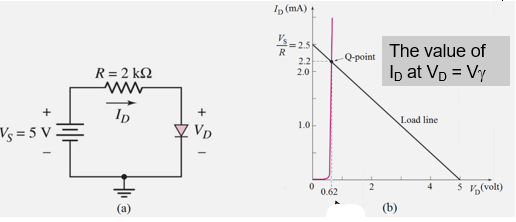
Applying KVL we get
2ID+ VD =5
ID = (VS-VD)/R
ID = (5-VD)/2
ID = -VD/2 +2.5
As we already know the working of p-n junction diode. As the temperature increases the covalent bond are broken which releases many electrons and protons. This increases the amount of current flow in the diode. The diode characteristics are shown below
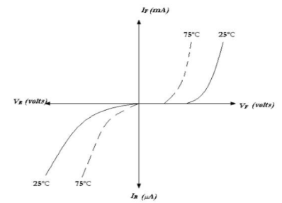
The above characteristics clearly shows that the forward characteristics are shifted upwards and reverse characteristics are shifted downwards with increase in temperature.
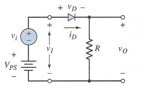
The total input voltage VI= dcVPS +acVi
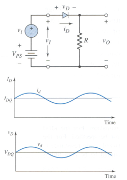
iD = IDQ+ id
VD = VDQ +Vd
iD=IS ( – 1)
– 1)  IS (
IS ( – 1)
– 1)
Diode current in terms of voltage is given as
ID=IS ( )
)
If vd<<VT

 1+
1+ 
The above relation can now be
iD = IDQ (1+  )= IDQ+( IDQ
 )
)
iD = IDQ+id
id= . vd = gdvd
vd= . id = rdid
For AC analysis diode is equivalent to resistor rd
rd=1/gd=
Where
VDQ = DC voltage
vd= ac component
id=total current
vD= total voltage
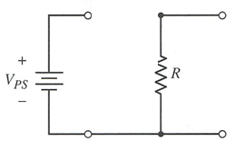
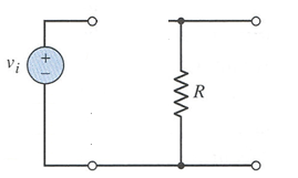
The DC and AC equivalent of diode is shown below
DC Equivalent
AC Equivalent
Q) For the circuit shown below

Given that VPS=9V, R=4kohm, VY = 0.6V and vi=0.2sinωt. Determine Vo and v0
Sol: For DC circuit vac=0 then the DC current is given as
IDQ = VDC-VY/R = 9-0.6/4000 = 2.1mA
The output dc component of voltage
V0=IDQ x R = 2.1x10-3 x 4000=8.4V
For AC Circuit VDC=0
Vi = idRd + idR
Rd= VT/IDQ = 0.026/2.1x10-3=12.38ohm
The AC diode current is
id = Vi/rd+R = 0.2sinωt/(4000+12.38) = 49.84sinωt  A
A
The output ac voltage of circuit is
v0 = idR = 49.84sinωt  Ax4kohm = 199.38sinωt mV
The diode depends on some parameters or ranges which need to be maintained while operating them. The few parameters are listed below
i) Semiconductor material: Mostly Si and Ge are used as semiconductor materials. Amongst the two Si is more common material to be used. The Si is widely used as they have low cost and high performance.
Ii) Diode type: According to the requirements the type of diode to be used is determined. For variable capacitance we use varactor diode. For voltage regulation we use Zener diode. The pn junction is used for rectification. Schottky diodes are used for low forward voltage.
Iii) Peak inverse voltage: The value of the voltage needs to me maintained to the permissible levels otherwise the device will fail. The PIV voltage is nothing but the maximum reverse voltage before breakdown. So, there needs to be a specific value maintained for smooth performance.
Iv) Forward Voltage Drop: Any electronics device passing current will develop a resulting voltage across it and this diode characteristic is of great importance, especially for power rectification where power losses will be higher for a high forward voltage drop. Also, diodes for RF designs often need a small forward voltage drop as signals may be small but still need to overcome it.
v) Reverse breakdown voltage: It is the reverse voltage in diode which needs to be maintained because after the limit of this voltage exceeds it cause irreparable damage to the circuit. If the voltage exceeds range of reverse voltage than high value of current flows damaging the whole circuit.
Vi) Maximum forward current: If the current in the circuit exceeds its maximum value large amount of heat is dissipated and it can damage the circuit. As diode in forward bias acts as short circuit and allows maximum forward current to flow in the circuit.
Vii) Junction temperature: It is also possible to calculate the junction temperature from a knowledge of the current, forward voltage drop and the thermal resistance. There should be margin between the junction temperature of diode and the package temperature.
Test using Multimeter
1) Select resistance mode in the multimeter with the help of selector switch.
2) Connect negative terminal of diode with negative end of multimeter.
3) Connect positive terminal of diode with positive end of multimeter.
4) Now check the reading shown, the multimeter should show a low value of resistance, because in forward bias the diode conducts. If the reading is high then the diode is faulty. If the diode is not faulty and shown low value, we continue the testing.
5) Connect negative terminal of diode with positive end of multimeter
6) Connect positive terminal of diode with negative end of multimeter
7) Now the multimeter should show high reading as the diode is reversed biased and very low current flows. If this this the case diode is good. If the multimeter shows low readings the diode is faulty.
- Zener diode is a special type of p-n junction semiconductor diode. In this diode, the reverse breakdown voltage is adjusted precisely between 3 V to 200 V.
- Its applications are based on this principle hence Zener diode is called as a breakdown diode.
- The doping level of the imparity added to manufacture the Zener diode is controlled in order to adjust the precise value of breakdown voltage.
PRINCIPLE OF OPERATION:
A Zener diode can be forward biased or reverses biased. Its operation in the forward biased mode is same as that of a p-n junction diode but its operation in the reverse biased mode is sustainably different.

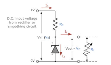
- The resistor, RS is connected in series with the Zener diode to limit the current flow through the diode with the voltage source, VS being connected across the combination. The stabilised output voltage Vout is taken from across the Zener diode.
- The Zener diode is connected with its cathode terminal connected to the positive rail of the DC supply so it is reverse biased and will be operating in its breakdown condition. Resistor RS is selected so to limit the maximum current flowing in the circuit.
- The load is connected in parallel with the Zener diode, so the voltage across RL is always the same as the Zener voltage, (VR = VZ).
- There is a minimum Zener current for which the stabilisation of the voltage is effective, and the Zener current must stay within the value operating under load within its breakdown region at all times.
- The upper limit of current is of course dependent upon the power rating of the device. The supply voltage VS must be greater than VZ.
- A Zener diode is always operated in its reverse biased condition. As such a simple voltage regulator circuit can be designed using a Zener diode to maintain a constant DC output voltage across the load despite variations in the input voltage or changes in the load current.
- The Zener voltage regulator consists of a current limiting resistor RS connected in series with the input voltage VS with the Zener diode connected in parallel with the load RL in this reverse biased condition.
- The stabilised output voltage is always selected to be the same as the breakdown voltage VZ of the diode.
Example:
A 5.0V stabilised power supply is required to be produced from a 12V DC power supply input source. The maximum power rating PZ of the Zener diode is 2W. Using the Zener regulator circuit above calculate:
a). The maximum current flowing through the Zener diode.
Maximum current = Watts/ Voltage = 2w/ 5V = 400mA
b). The minimum value of the series resistor, RS
Rs = Vs – Vz/ Iz = 2 – 5 / 400mA = 17.5 Ω
c). The load current IL if a load resistor of 1kΩ is connected across the Zener diode.
IL = Vz / RL = 5v/ 1000Ω = 5mA
d). The Zener current IZ at full load.
IZ = Is – IL = 400 mA – 5mA = 395mA
- It is the simplest form of the rectifier. Here, a single diode is used.
- It consists of an AC source, transformer (step-down), diode, and resistor (load).
- The diode is placed between the transformer and resistor (load).
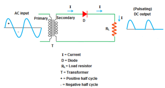
Operation:
- It allows only half cycle and blocks the other half cycle.
- When it allows positive half cycles and blocks negative half cycles, it is called a positive half wave rectifier. The output DC current or DC signal produced by a positive half wave rectifier is a series of positive half cycles or positive sinusoidal pulses.
- When it allows electric current during the negative half-cycle of input AC signal and blocks electric current during the positive half-cycle of the input AC signal.
- A negative half wave rectifier produces a series of negative sinusoidal pulses.
- For an ideal diode, the positive half cycle or negative half cycle at the output is exactly same.
Characteristics of half wave rectifier
Ripple factor
The ripple factor is given as

Finally, we get
γ = 1.21
Hence, the DC voltage is 121% of the DC magnitude.
DC current
The DC current is given by,

Where,
Imax = maximum DC load current
Output DC voltage (VDC)
The output DC voltage is given by,

Where, VSmax = Maximum secondary voltage
Rectifier efficiency
It is defined as the ratio of output DC power to the input AC power.
The rectifier efficiency of a half wave rectifier is 40.6%
Root mean square (RMS)
The root mean square (RMS) value of load current in a half wave rectifier is

The root mean square (RMS) value of output load voltage in a half wave rectifier is

Form factor
It is defined as the ratio of RMS value to the DC value given by,
F.F = RMS value / DC value
The form factor of a half wave rectifier is F.F = 1.57
Advantages:
- Very few components are used. So, the cost is very low.
- Easy to construct
Disadvantages:
- Loss of power
- Pulsating direct current
- Produces low output voltage.
Key Takeaways:
- It allows only half cycle and blocks the other half cycle.
- When it allows positive half cycles and blocks negative half cycles, it is called a positive half wave rectifier and vice-versa.
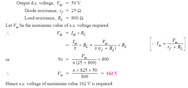
Q. A half-wave rectifier is used to supply 50V d.c. To a resistive load of 800 Ω. The
diode has a resistance of 25 Ω. Calculate a.c. Voltage required.
Solution:
Types on the basis of construction:
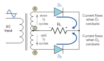
- Center-taped transformer
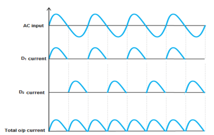
It consists of two power diodes connected to a single load resistance (RL) and each diode supply current to the load one by one. When point A of the transformer becomes positive, diode D1 conducts in the forward direction.
When point B becomes positive (for the negative half of the cycle) with respect to point C, diode D2 conducts and the current starts flowing through resistor R is in the same direction for both half-cycles.
As the output voltage across the resistor R is the sum of the two waveforms combined, this type of circuit is also called as a “bi-phase” circuit.
The spaces present between the frequency response of each half-wave developed by each diode is now being filled in by the other therefore, the average DC output voltage across the load resistor becomes double that of the single half-wave rectifier circuit.
2. Bridge Rectifier
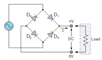
It uses four individual rectifying diodes which are connected in a closed loop called “bridge” configuration to produce the desired output.
It does not require a special centre tapped transformer, hence reducing its size and cost. The single secondary winding is connected one side to the diode bridge network and the other side to the load.
The four diodes D1 to D4 are arranged in “series pairs” and only two diodes conduct current during each half cycle.
During the positive half cycle, diodes D1 and D2 conduct in series while diodes D3 and D4 are reverse biased producing current through the load.
During the negative half cycle, diodes D3 and D4 conduct in series and diodes D1 and D2 are switched “OFF” as they become reverse biased producing current through the load.
During each half cycle the current flows through two diodes instead of just one. The ripple frequency is now twice the supply frequency.
Output Waveform:
Characteristics of full wave rectifier
Ripple factor
The ripple factor is given by

Finally, we get γ = 0.48
Rectifier efficiency
It is defined as the ratio of DC output power to the AC input power.
It can be mathematically written as
η = output PDC / input PAC
The rectifier efficiency of a full wave rectifier is 81.2%.
Peak inverse voltage (PIV)
It is the maximum voltage a diode can withstand in the reverse bias condition.
The peak inverse voltage (PIV) = 2Vsmax
DC output current
The current produced by D1 is Imax / π and the current produced by D2 is Imax / π.
So, the output current IDC = 2Imax / π
Where, Imax = maximum DC load current
DC output voltage
The DC output voltage appeared at the load resistor RL is given as
VDC = 2Vmax /π
Where,
Vmax = maximum secondary voltage
Root mean square (RMS) value of load current IRMS
The root mean square (RMS) value of load current in a full wave rectifier is

The root mean square (RMS) value of output load voltage in a full wave rectifier is

Form factor
It is the ratio of RMS value of current to the DC output current
F.F = RMS value of current / DC output current
The form factor of a full wave rectifier is F.F = 1.11
Advantages:
- High rectifier efficiency
- Low power loss
- Low ripples
- It has fewer ripples than the half wave rectifier.
Disadvantages:
- High cost
- The center tapped transformers are expensive and occupy a large space.
Key Takeaways:
- The process of converting the AC current into DC current is called rectification.
- When an additional wire is connected across the exact middle of the secondary winding of a transformer, it is known as a center tapped transformer.
- Bridge rectifier uses four individual rectifying diodes connected in a closed loop “bridge” configuration to produce the desired output.
Q. A full-wave rectifier uses two diodes, the internal resistance of each diode may
be assumed constant at 20 Ω. The transformer r.m.s. Secondary voltage from center tap to each end of secondary is 50 V and load resistance is 980 Ω. Find: (i) the mean load current (ii) the r.m.s. Value of load current.
Solution:

(i) 
(ii) 
2.12.1 RC Filters
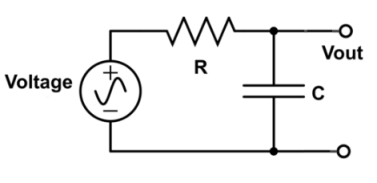
RC circuit consists of resistors and capacitors which allows a certain amount of signal frequency and rejects unwanted signal.
The functioning of circuit depends on the required cut off frequency.
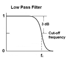
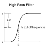
Cut off frequency is the frequency above or below which the output power decreases to the one half the pass band power usually referred to as 3dB point.
Low pass filter is a circuit which passes only low frequency signals and attenuates high frequency signals and it is determined by the RC time constant.
At high frequencies the capacitor offers less amount of reactance and hence the output decreases as frequency increases.

Where Xc=Capacitive reactance measured in ohms, f = frequency in hertz, C = capacitance in farad.
When f = 0 Xc = ∞ (Open Circuit) Xc = 0 (Short Circuit)
LOW PASS RC CIRCUIT AS AN INTEGRATOR:
An integrator depends upon the time constant of the RC circuit.
The time constant is large enough as compared with the input signal so that the capacitor charges slowly and the input voltage is applied across the resistor.
Here, the output is an integral function of the input voltage and is given by,
The output equation is given by the equation Vo = 1 / c
Frequency Response:
HIGH PASS CIRCUIT AS DIFFERENTIATOR:
The high pass circuit acts as a differentiator depending upon the time constant of the RC network.
It varies depending upon the circuit.
The time constant of the circuit is small and the capacitor charges quickly as all the voltage is taken by the capacitor and small amount of voltage appears across the resistor.
The current in the circuit is decided by the capacitance.
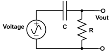
The output equation is given by: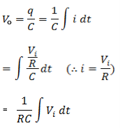
Frequency Response:
Key Takeaways:
- Cut off frequency is the frequency above or below which the output power decreases to the one half the pass band power usually referred to as 3dB point.
- Low pass filter is a circuit which passes only low frequency signals and attenuates high frequency signals when passed through a network over certain cut off frequency and it is determined by the RC time constant.
2.12.2 LC Filters
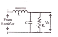
Here, inductor L is in series and shunt capacitor C is connected with load.
The choke (L) i.e. inductor allows the dc component to pass through it because its dc resistance R is very small.
It acts as open circuit and the capacitive reactance Xc is very high for dc.
All dc current that passes through dc output voltage is obtained.
The inductive reactance XL = 2pfL is high for ac components.
Therefore, the ripples are reduced.
Waveform:

Advantages:
- In choke input filter, current flows continuously. Therefore, the transformer is used more efficiently.
- Ripple content at the output is low.
- It is less dependent on the load current.
- DC voltage drop across L is much smaller because its de resistance R is very small.
Disadvantages:
- Large size and weight of inductors,
- More cost,
- External hold is produced by inductor.
Key Takeaways:
- The inductive reactance XL = 2pfL is high for ac components.
- Inductor L is in series and shunt capacitor C is connected with load.
They are used more due to less cost and are effective. Zener diode is used for voltage regulation in the circuit. At maximum load current the shunt regulator draws virtually no current and at minimum load current, the shunt voltage regulator passes the full current. Zener diode a shunt regulator is shown below.
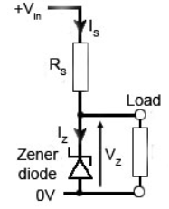
There is voltage drop across the resistor in series to the source. The voltage across the Zener diode is maintained irrespective of the change in current. It takes up the current variations required to ensure the correct drop across the series resistor. In this way it shunts sufficient current to maintain the voltage across its terminals and hence the load.
It is an open loop connection. Shunt voltage regulators are not particularly effective or efficient in high current situations. The simple Zener diode voltage regulator, when used as a low current voltage reference is widely used, and its inefficiency can be tolerated in view of the low current.
2.14.1 LED
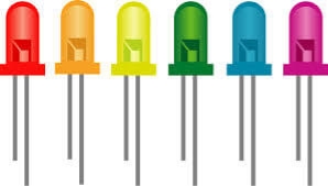
Light Emitting Diodes (LEDs) are the most widely used semiconductor diodes.
It emits either visible light or invisible infrared light when forward biased.
It is an optical semiconductor device that emits light when voltage is applied. It converts electrical energy into light energy.
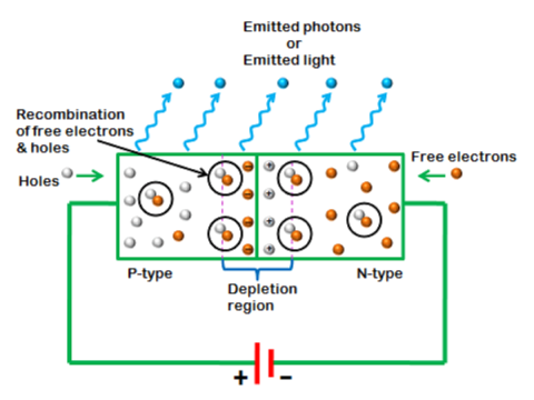
When LED is forward biased, free electrons in the conduction band recombines with the holes in the valence band and releases energy in the form of light.
The process of emitting light in response to the strong electric field or flow of electric current is called electroluminescence.
It works only in forward bias condition. When LED is forward biased, the free electrons from n-side and the holes from p-side are pushed towards the junction.
When free electrons reach the junction or depletion region, some of the free electrons recombine with the holes in the positive ions.
The current flowing through the LED is mathematically written as

Where,
IF = Forward current
VS = Source voltage or supply voltage
VD = Voltage drop across LED
RS = Resistor or current limiting resistor
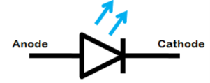
Symbol
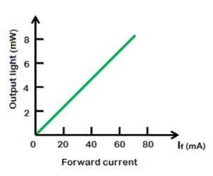
Output characteristics of LED
Advantages :
- LEDs are very cheap and readily available.
- LEDs are light in weight.
- Smaller size.
- LEDs have longer lifetime.
- LEDs operates very fast.
Applications:
- Calculators
- Picture phones
- Traffic signals
- Digital computers
- Multimeters
2.14.2 LCD
LCD DISPLAY
The liquid crystals are used to produce a visible image. Liquid crystal displays are super-thin technology display screens that are generally used in laptop computer screens, TVs, cell phones and portable video games. Light is projected from a lens on a layer of liquid crystal. This combination of colored light with the grayscale image of the crystal (formed as electric current flows through the crystal) forms the colored image. This image is then displayed on the screen.
When current is applied to liquid crystal molecule they untwist. This causes the angle of light which is passing through the molecule of the polarized glass and also cause a change in the angle of the top polarizing filter. They work on principle of blocking light. The electrode panel of indium-tin-oxide is kept on top and polarized glass with a polarized film on the bottom. This is enclosed by common electrode. Then completely covered by liquid crystal. When there is no current, the light passes through the front of the LCD it will be reflected by the mirror and bounced back. As the electrode is connected to a battery the current from it will cause the liquid crystals between the common-plane electrode and the electrode shaped like a rectangle to untwist. Thus, the light is blocked from passing through. That particular rectangular area appears blank.
2.14.3 Seven Segment Display
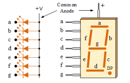
The 7-segment display shows seven segments. The seven segment allows us to display decimal numbers from 0 to 9. Below shown is the 7-segment LED with its truth table.


The segments can be light by forward biasing them properly in correct sequence and the other which are dark tighter make the proper desired number to be displayed. The displays common pin is generally used to identify which type of 7-segment display it is. As each LED has two connecting pins, one called the “Anode” and the other called the “Cathode”, there are therefore two types of LED 7-segment display called: Common Cathode (CC) and Common Anode (CA).
Common Cathode (CC): In this case all the cathode connections are connected to ground. The individual segment is turned ON by high logic.
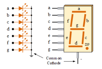
Common Anode (CA): In this all the anode of LED are joined to logic 1. The individual segment is light up by applying 0 logic. These displays are generally used. For instance, to display the numerical digit 0, we will need to light up six of the LED segments corresponding to a, b, c, d, e and f.
References:
1. David A Bell, Electronic Devices and Circuits Oxford Higher Education, 5th Edition,
(2017).
2. NN Bhargava, DC Kulshreshtha, SC Gupta, Basic Electronics and Linear circuits,
Tata McGrawHill Publishing Company, 2nd Edition, (2013).