Module 4
Fabrication of Semiconductor Devices and ICs
Usually Si and Ge are used as the semiconductors. But amongst the two SI is more common. Si is easily available. Si s available as silicon dioxide and mixture of Si with other materials. From zinc and copper ores Ge is derived. These semiconductors contain large impurities and hence need to be refined. After they are refined, they are present in polycrystalline form. So, they are converted to single crystal material. All the atoms of which are arranged into a single pattern. At final manufacturing stage both Si and Ge are of single crystal bar which are 30cm long. The bar is sliced into wafers of disc shape with thickness of 0.4cm.
The semiconductor wafers for processing are heated by the means of radio frequency heating coils. The n-type wafer is diffused with a p-type material by placing in a high temperature such that the outer layer of n-type is converted to p-type. This is called Diffusion.
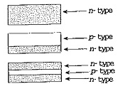
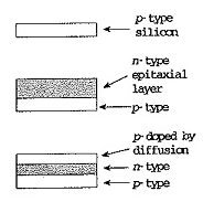
There is one more method called as Epitaxial Growth in which the semiconductor wafers are contained in gas surrounding the wafer. The semiconductor atoms in the gas accumulate on the wafer forming a thin layer. The layer can be of p-type or n-type depending on the impurity content of gas.
The process of diffusion and alloy methods ate used for fabrication of diode. For making pn-junction diode a tiny pellet of impurity can be p-type or N-type is melted on the surface of n-type crystal.
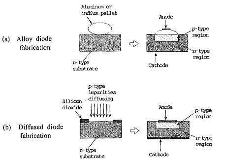
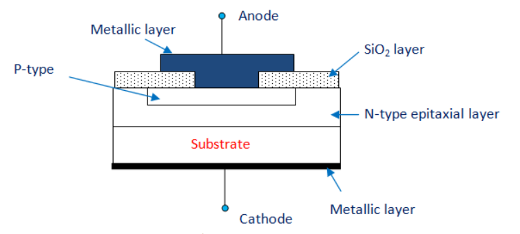
In Diffusion an n-type semiconductor is heated in the atmosphere which has acceptor impurities present in vapour form. Due to this some of the impurities form a layer and sets on the n-type crystal. By this process p region is created on n type material. The area in which the acceptor impurity is required is left uncovered else all is covered. The other way is Epitaxial growth in this a thin layer of high impurity layer of semiconductor is developed on heavily doped substrate. Si02 layer is thermally grown on the top surface, photo-etched and then aluminium contact is made to the P- region. A metallic layer at the bottom of the substrate forms the cathode to which lead is attached.
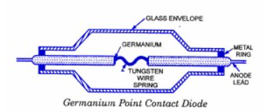
An N-type Ge/Si wafer of 12.5mm2x0.5mm thickness is taken. A metal base is soldiered to one side by RF heating and other side has phosphorous spring attached. The point contact now has a barrier layer around it due to the pulsating current forming. Then around the wire a p-region is formed and the wire is N-type resulting in pn-junction formation. This is called point contact technique.
Diode Packing:
According to the use and requirements the diodes are packaged in different sizes. Few of them are shown below
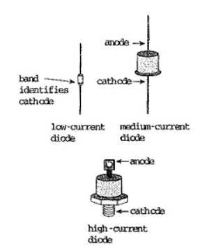
The above figure shows various diodes according to the current required which is low, medium and high. The power transistor type package and rectifier formed by four diode connection is shown.
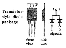
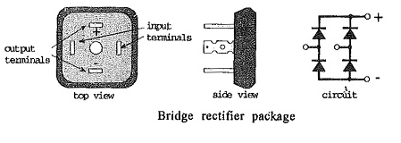
The techniques are listed below
i) Current Gain: When large amount of charge carriers pass to collector through emitter current gain is high. So, the base in this case should be lightly doped and very narrow compared to emitter and collector.
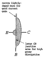
Ii) High Power: For high power the transistor needs to have large E-B surface so that required amount of charge carriers can flow. As shown in above figure.
Iii) Frequency Response: For high frequency response the transistor must have very narrow base region in order to allow minimum charge carrier to flow. As for high power we need large area for EB and in this case we need narrow base junction to meet both requirements the EB junction is long thin zig-zag strip.
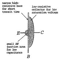
Iv) Switching Transistor: There has to be low junction capacitance in order to achieve fast switching. It should also have low saturation voltage and short storage time. The collector region must have low resistivity. The charge carriers in depletion region of CB junction must have faster combination to achieve short storage time.
v) Breakdown and Punch-Through: The reverse breakdown voltage is limited by the collector as CB is reverse biased. The base and collector must be lightly doped to get high breakdown voltage. The base should not be lighter than the collector because if this is the case the depletion region will penetrate into base and will cause breakdown due to punch through when connected to EB.
There are five ways of fabrication as explained below:
i) Diffusion Technique: In this method the N-type wafer is heated at high temperature in closed region containing vapours of P-type impurities. The p-type impurities are deposited over the N-type resulting in N-P junction. Again, the whole assembly is kept in the atmosphere of N-type vapours. The N-P junction is kept uncovered for the part which need N-type impurities to deposited, rest is covered. The vapours gets deposited on the p region forming NPN. This is explained with figure below.

Ii) Point contact Technique: In this technique N-type wafer is taken its one end is soldered to metallic base and the other to the tungsten spring. Then a large amount of current is passed for a millisecond so that pn junction is created.
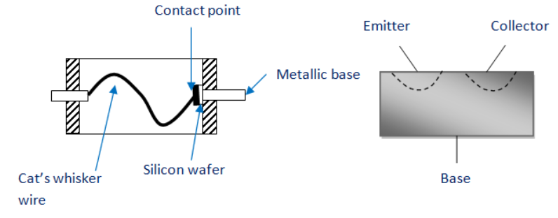
Iii) Alloy/Fused Technique: In this technique N-type wafer is taken and two tiny dots of indium or aluminium are made on opposite side of wafer. This arrangement is heated to a high temperature. The temperature needs to be lower than melting point of acceptor. Due to this temperature some part of indium dissolves and penetrates in N type wafer forming PNP transistor.
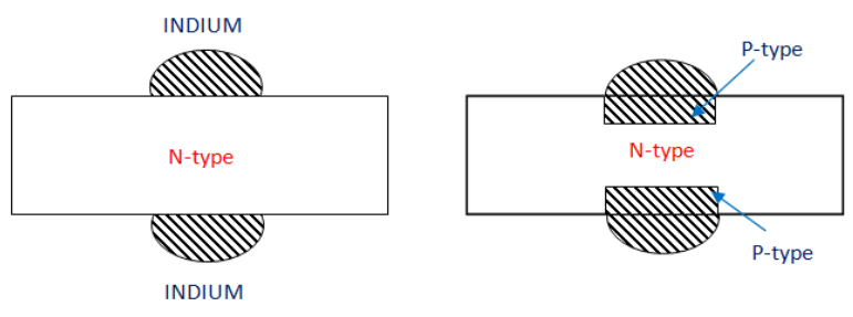
Iv) Rate-Grown Technique: Here floating technique is used through which a single crystal is drawn from melt of Ge/Si having p-type impurities. A single semiconductor seed is submerged in molten semiconductor and is slowly taken out in slow rotation through rod holding it. Initially p-type impurities are added and then N-type.
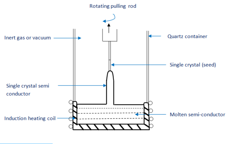
v) Epitaxial Technique: A N-type layer is grown on a substrate. The layer formed can be of E, B or C. The figure is shown below.
Integrated circuits are those circuits in which the electronic circuits are not separable. In IC number of semiconductor devices like diode, transistor and capacitors are fabricated permanently. They are also known as chip or microchip. This technology was invented in the year of 1950 the by Jack Kilby of Texas Instruments USA and Robert Noyce of Fairchild Semiconductor USA. The first costumer to this new invention was the US Air Force. In the year 2000 Jack Kilby won the Nobel Prize in Physics for miniaturized electronic circuits. One and a half years after Kilby demonstrated his IC design, Robert Noyce of Fairchild Semiconductor Limited came up with his own integrated circuit.
There are two types of ICs
i) Analog IC: Here both input and output signals are continuous. The output signal depends on the input signal and is linear function of input. The most common analog IC are amplifiers, comparators, timers and voltage regulators.
Ii) Digital IC: The digital IC are logic gates, microprocessors. They operate on binary data 0,1 or 0V and +5V.
The main component of ICs are transistors. They can be BJT of FET as per the requirements and applications. There are five groups of IC categorised on the basis of number of transistors being used in that IC.
i) SSI (Small Scale Integration): The number of transistors in one chip are up to 100.
Ii) MSI (Medium Scale Integration): The number of transistors in one chip are from 100-1000.
Iii) LSI (Large Scale Integration): The number of transistors in one chip are from 1000-20000.
Iv) VLSI (Very Large-Scale Integration): The number of transistors in one chip are from 20000-1000000.
v) ULSI (Ultra Large-Scale Integration): The number of transistors in one chip are from 1000000-10000000.
The IC manufacturing technology is of two types
i) Monolithic: In this all components are interconnected in a single chip.
Ii) Hybrid: In this type separate components are attached on a ceramic substance and interconnected by wire or metallization pattern.
The IC packaging is of two kinds
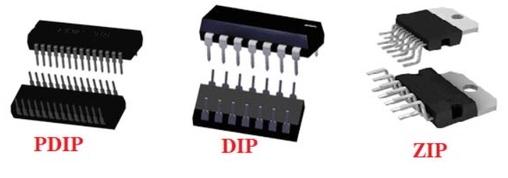
i) Through-hole mount packaging: In this type of design the pins are on one side of the board and other is smouldered. Dual in line package [DIP] is one of its type and most commonly used. They come in ceramic and plastic types. The number of pins ranges from 4-64. The DIP is of many types such as plastic dual in line package [PDIP] and Molded Dual in line package [MDIP]. There are zigzag in line package [ZIP] which have pins inserted perpendicular to the circuit board and are closer to each other. In standard packages the ping are 0.1” apart.
Ii) Surface Mount Packaging: In this the component s directly placed on the PCB. This fabrication process is faster than the above. The package like small outline L-leaded package have gull-wings that draw out in L shape and mounted directly on the board. The Ball grid array have ball arrays soldered on back side of PCB. The fine pitch land grid array has solder land arrays on back of PCB.
It is the unit for measurement of power. It is denoted by base 10 logarithm ratio. When circuit is analysed in frequency domain then comparing the ratio of amplitude values at input and output is easy on the log scale. The unit decibel is commonly used to show the ratio of power change. Let the two powers be P1 the input power and P2 the output power, then the ratio in decibel is given as
DB = 10log10[P2/P1]
The term decibel is not power it is comparison of two powers.
DB RULES OF THUMB:
Double the power: +3 dB
Halve the power: -3 dB
Ten times the power: +10 dB
One tenth the power: -10 dB
100 times the power: +20 dB
1/100 the power: -20 dB
Q) An audio amplifier delivers 150 watts into an 8ohm speaker load when fed by a 150mW input signal. Calculate the power gain of the amplifier in decibels.
Sol: Power Gain = 10log10[P2/P1]
= 10log10[150/0.150] = 30dB
Q) A 100watt audio amplifier has a power gain ratio of 30dB. What will be its maximum input value?
Sol: Power Gain = 10log10[P2/P1]
AP=10log10[P2/P1]
Antilog (AP/10) = 100/P1
100/P1 = 103
P1 = 100/1000 = 0.1W or 100mW
References:
1. David A Bell, Electronic Devices and Circuits Oxford Higher Education, 5th Edition,
(2017).
2. NN Bhargava, DC Kulshreshtha, SC Gupta, Basic Electronics and Linear circuits,
Tata McGrawHill Publishing Company, 2nd Edition, (2013).