Module 1
Basic Semiconductor and PN Junction Theory
The smallest piece of an element is called an atom. An atom can be further divided into proton, neutron and electron. Centre of an atom is nucleus. It consists of proton and neutron. Electrons revolve around the nucleus in certain orbits. Electrons are negatively charged with magnitude of -1.6x10⁻¹⁹ coulombs and protons are positively charged with magnitude of +1.6x10⁻¹⁹ coulombs. The neutrons are uncharged and hence an atom is electrically neutral.
The total number of electrons and protons is equal to the atomic number and total number of protons and neutrons is equal to the mass of atom. The electrons revolve around the nucleus in different orbits or shells. The number of maximum electrons in any orbit is given as 2n2. Where n=number of orbits in which the electron is present. The electrons in the outer most orbit is called as valence electrons.
The nucleus of an atom is positively charged. The electrostatic force between the electron and proton is equal to the centrifugal force developed by orbiting of electrons making atom stable. The outer orbit has more energy than the inner orbit hence when the electron jumps from outer to inner orbit energy is released and if electron jumps from inner to outer obit the energy is absorbed.
According to Neil Bohr’s theory of atomic structure all atoms have different energy levels. When two or more atoms are placed near to each other their energy levels get transformed to energy band structure. These energy bands are formed due to mutual interaction between the atoms caused by the electromagnetic force between them.
The below figure shows the energy bands of various energy levels. The electrons nearer to nucleus of interacting atom are having energy band 1 and those in outer orbit have E2, E3 so no.

Fig: Energy band in crystal
Energy band in crystals can of different types which are
i) Valence Band: The electrons in the outer most orbit of an atom is present in this energy band. This is the highest energy band at room temperature. This band can be completely or partially filled.
Ii) Conduction Band: This is the lowest energy band containing electrons which are free from the attractive force of atom’s nucleus.
The Valence band has low energy level than conduction band. This is the reason that CB is above the VB separated by energy gap.
Energy Band Structures in Metals, Semiconductors and Insulators
Below shown is the figure of energy band for metals, semiconductors and insulators. The conduction in materials is possible only because of the electrons present in the conduction band.
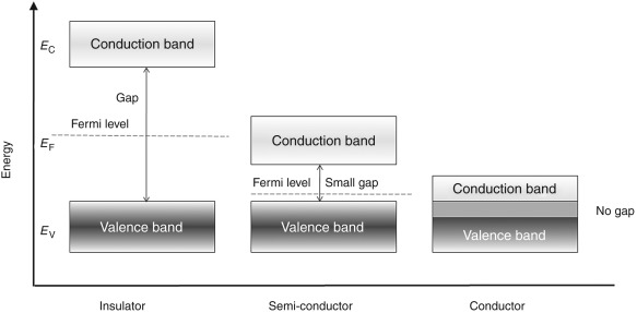
Fig: Energy band for Conductors, Semi-conductors and Insulators
From the above figure the conductors (metals) have both the energy bands overlapping. This shows that they have large number of free electrons which make them the good conductors.
There is one more energy band shown above having a huge gap between CB and VB which significantly shows that we need to provide large amount of energy to the electrons to jump from VB to CB. But this amount of energy is not possible to be applied and hence no movement of electron is seen. There is no conduction possible making them insulators.
The last one seen from above figure has a difference in CB and VB but the energy gap is such that after applying external voltage some of the electrons can jump from VB to CB. These are semi-conductors which can be made to conduct as conductors by exciting them externally.
1.3.1 n-Type semiconductors
To increase the number of conduction band electrons intrinsic silicon, pentavalent imparity atoms are added. These are atoms with five valence electrons such as
i) arsenic (As)
Ii) phosphors (P)
Iii) Bismuth (Bi)
Iii) Antimony (Sb)
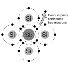
- Pentavalent impurity atom in a silicon crystal. An antimony (sb) impurity atom shown above-
- Each pentavalent atom forms covalent bonds with four adjustment silicon atoms, leaving one extra electron.
- The pentavalent atom gives up on electron, it often called a donor atom.
- Majority and minority carriers: A type here mean negative charge of an electron. Electrons are called the majority carriers in n-type material.
- Hole in an n-type material are called minority carriers
1.3.2 p-Type semiconductors
To increase the number of holes in intrinsic silicon, trivalent impurity atoms are added. These are atoms with three valence electrons such as
i) Boron(B)
Ii) Indium (In)
Iii)Gallium (Ga)
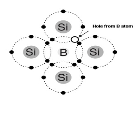
- Trivalent impurity atom in a silicon crystal structure. A) boron (B) impurity atom is shown in the center.
- The number of holes can be carefully controlled by the number of trivalent impurity atoms added to the silicon.
- A Hole created by the doping process is not accompanied by a conduction (free) electron.
- Trivalent Atom can take an electron it is often referred to as on accepted atom
The conductivity of a material depends upon the concentration of free electrons. In semiconductors the concentration of electrons is in between conductors and insulators. As discussed in earlier section that the conduction in semiconductor is possible up to some temperature. Germanium and silicon are generally used semiconductors. If we talk about Ge than it has 4 electrons in its outer most shell which can form covalent bond with four adjacent Ge atoms.
At absolute zero the semiconductors behave as insulators as there are no free electrons for conduction. At room temperature due to presence of some energy few covalent bonds break and there are some free electrons. These free electrons contribute in conduction. For Ge the energy required to break the covalent bond is 0.72eV. For Si the energy required to break the covalent bond is 1.1eV at room temperature.
In semiconductors the holes can also be considered as the carrier of electricity. The hole exists in semiconductors where there is incomplete bond. When an electron leaves its place and to form bond with neighbouring atom it creates a new hole at that place. This process continues as every time due to electrons a new hole is created. So, it can be visualized as the holes move in opposite direction to the electrons. In ideal case the semiconductor has equal number of holes and electrons.
The current density due to drift holes for applied field E is given as
Jh= q p pE
pE
The current density due to drift electrons for applied field E is given as
Je = q pn n E
n E
The drift current density is given as
J= Jp+Jn
J = q (p p+n
p+n n) E
n) E
J= E
E
 = q (p
 p+n
p+n n)
n)
Where
 = Conductivity of semiconductors
n, p = magnitude of free electron and hole concentration respectively.
Q1) For a p-type Ge ni = 2.1x10¹⁹m-3 density of boron =3.2x10²³ atoms m-3. The electron and hole mobility are 0.4 and 0.2 m2V-1s-1. Calculate conductivity before and after addition of boron?
Sol: Before adding boron
 = q (p
 p+n
p+n n)
n)
= ni q ( p+
p+ n) = 2.1x1019x1.6x10-19x(0.4+0.2)=2.016 S/m-1
After adding boron
 = q p
= q p p
p
= 3.2x1023x1.6x10-19x0.2=10.24x10³S/m-1
Q1) Determine the density of the donor atoms which have been added to the intrinsic Ge to make it a n-type material of resistivity 0.1x10⁻²ohm-m. Mobility of electron in n-type semiconductor is 0.5m2V-1s-1.
Sol:  = q (n
 n)
n)
n=  /q
/q n
n
 = 1/
= 1/
n= 1/ q
q n = 1/(0.1x10-2x0.5x1.6x10-19) = 1.25x10²²m-3
Q2) The intrinsic carrier density at room temperature in Ge is 3.4x10¹⁹m-3. If electron and hole mobilities are 0.4 and 0.2 m2V-1s-1 respectively. Calculate its resistivity?
Sol:  = 1/
= 1/
 =ni q (
 p+
p+ n) = 3.4x1019x 1.6x10-19(0.4+0.2) = 3.264S/m-1
 = 1/
= 1/ = 1/3.264 = 0.31ohm-m
Q3) The electron and hole mobilities in In-Sb are 6 and 0.2 m2V-1s-1 respectively. At room temperature resistivity of In-Sb is 2x10⁻⁴ohm-m. Find intrinsic carrier concentration assuming the material to be intrinsic?
Sol:  = 1/
= 1/
 =ni q (
 p+
p+ n)
n)
ni = 1/  q (
q ( p+
p+ n) = 1/2x10-4x1.6x10-19(6+0.2) = 5.04x10²¹m-3
Q4) An electric field of 90Vm-1 is applied to n-type semiconductor. Determine the current density in sample given electron mobility 0.4 m2V-1s-1, n=5.9x10²⁰m-3?
Sol: J= E
E
 = nq
= nq n = 5.9x1020x1.6x10-19x0.4=37.36S/m-1
J=3.39x10³
Q5) Determine the density of the donor atoms which have been added to the intrinsic Ge to make it a n-type material of resistivity 0.5x10⁻²ohm-m. Mobility of electron in n-type semiconductor is 0.8m2V-1s-1.
Sol:  = q (n
 n)
n)
n=  /q
/q n
n
 = 1/
= 1/
n= 1/ q
q n = 1/(0.5x10-2x0.8x1.6x10-19) = 1.56x10²¹m-3
When a semi-conductor is doped such that half the portion is doped with the trivalent impurity (Al, Ar, Bi) and the other half is doped with pentavalent impurity (B, P) then the junction formed is known as PN junction.

Its symbol is

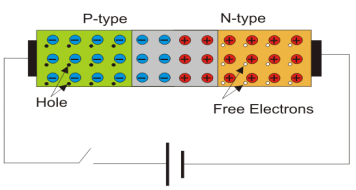
Forward Biased P-N Junction
When p-type region is connected with the positive terminal and n-type region with the negative terminal of the voltage source, then the junction is said to be forward biased.
At this condition, due to the attraction of cathode, electrons create covalent bond in p-type material and are attracted towards the terminal.
Hence, numbers of covalent bonds are broken and electrons moves towards the positive terminal increasing the concentration of electrons in the crystal nearer to the terminal and these electrons recombine with holes here.
In this way, the number of holes increases in the p-type region away from the junction, and it is reduced in the portion of p-type region nearer to the terminal.
Due to the higher concentration of holes adjacent to negative impurity ions layer the electrons of negative ions come out and recombine with those holes and create new holes in the layer.
Consequently, the width of this negative ions layer is reduced and finally this layer vanishes.
Reverse Biased PN Junction
When positive terminal is connected to the n-type region and the negative terminal is connected to the p-type region then the pn junction is said to be in reverse biased condition.
When no voltage applied across the p n junction, the potential developed across the junction is 0.3 volts at 25oC for germanium and 0.7 volts at 25oC for silicon p n junction.
The polarity of this potential barrier is same as the polarity of voltage source applied during reverse biased condition.
Now if reverse biased voltage is increased the barrier potential developed also increases. Hence, the pn junction widens.
The free electrons of the n-type region are attracted towards positive terminal of the source because of that more positive impurity ions are created in the depletion layer which makes the layer thicker.
At the same time, electrons are injected in the p-type region. Due to the positive potential of the n-type region the electrons are drifted towards the junction and combine with holes and create more positive impurity ions in the layer.
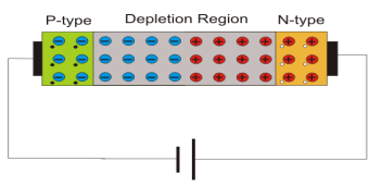
Key Takeaways:
- The free electrons from the negative terminal of the battery continue to pour into the n-region while the free electrons in the n-region move towards the junction.
- The electrons travel through the n-region as free electrons hence, current in n-region is by free electrons.
- When these electrons reach the junction, they combine with holes and become valence electrons.
- As valence electron, they move through the holes in the p-region, hence, current in the p-region is by holes.
- When these valence electrons reach the left end of the crystal, they flow into the positive terminal of the battery.
When the diode is not biased a natural potential barrier is developed across the depletion region which is of 0.5-0.7V for Si and 0.2-0.3V for Ge diodes.
When the diode is forward biased the thickness of depletion region reduces (VD>0) and the diode acts like a short circuit. There is large amount of current flowing due to this short circuit.
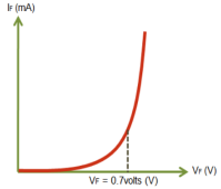
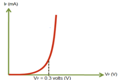
When the diode is reverse biased the thickness of depletion region increases (VD<0) and the diode acts as an open circuit. There is high voltage and no current dure to open circuit.
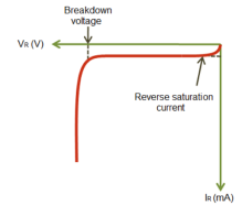
The diode current equation is given as
I=I0 ( – 1)
– 1)
I = diode current
I0 = Saturation current
Q=charge
V=Voltage applied across diode
K= Boltzmann constant=1.38x10⁻²³ JK-1
T= temperature in kelvin
For forward biased diode large amount of current flows so the above equation becomes
I=I0 ( )
)
As the current is large so 1 is neglected.
For reverse biased diode the exponential term is neglected so the current equation becomes
I=I0
References:
1. David A Bell, Electronic Devices and Circuits Oxford Higher Education, 5th Edition,
(2017).
2. NN Bhargava, DC Kulshreshtha, SC Gupta, Basic Electronics and Linear circuits,
Tata McGrawHill Publishing Company, 2nd Edition, (2013).