Module 3
Bipolar Junction Transistors and Electronic measuring instruments
BJT: The BJT is constructed with the three draped semiconductors region’s separate by two PN junctions as shown below
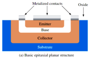
-Basic epitaxial planner structures.
-Three terminal with region’s are called emitter, base and collector.
-The physical representation of the two types of BJT’s,
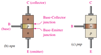
One type consists between two regions separated by a P region (npn) and other type consists of two p regions separated by an n region (pnp).
-The Pn junction joining the base region and the emitter region is called the base emitter junction.
-The Pn junction joining the base region and the collector region is called the base collector junction.
-The base region is lightly doped and very thin compared to the heavily doped emitter and the moderately doped collector regions.
Transistor Current:-
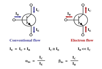
Transistor’s Characteristic’s and parameters:-
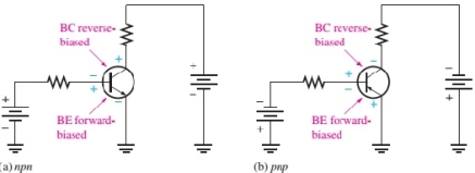
-The transistors is connected to d.c bias vtg for both the npn & pnp types VBB forward biases the base emitter junction &Vcc reverse biases the base collector junction.
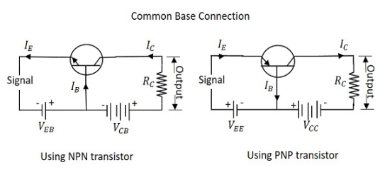
*Biasing conditions for different regions of operation:-
Sr. No | Region of operation | BE junction | CB junction | Work |
1 | Cut-off region | R.B | R.B | S/w |
2 | Active region | F.B | R.B | Ampr |
3 | Saturation region | F.B | F.B |
|
Transistor’s Configuration:-
1) Common Base configuration(C.B)
2) Common emitter Configuration(C.E)
3) Common Collector Configuration(C.C)
Q) In a CB IE= 2mA, IC=1.5mA. Calculate IB?
Sol: IE =IB+IC
2= IB+1.5
IB=0.5mA
Q) In a CB current amplification factor is 0.9. If emitter current is 1.2mA. Determine the value of base current?
Sol: α = 0.9
IE =1.2mA
α = IC/ IE
IC = α IE =0.9 x 1.2 = 1.08mA
IE =IB+IC
1.2= IB+1.08
IB= 0.12mA
Q) In a CB connection IC=1.0mA and IB= 0.02mA. Find the value of current amplification factor?
Sol: IE =IB+IC =1+0.02 = 1.02mA
α = IC/ IE
α = 1.0/1.02 = 0.98
Q) In a CB connection the emitter current is 0.98mA. If the emitter circuit is open the collector current becomes 40 A. Find total collector current. α =0.92
Sol: ICBO=40 A
A
IC = α IE+ICBO
= (0.92 x 0.98x10-3) + 40x10-6
IC =0.94mA
Q) In a common base connection, α = 0.95. The voltage drop across 3 kΩ resistance which is connected in the collector is 2.5 V. Find the base current.
Sol: IC = 2.5/3000 = 0.83mA
α = IC/ IE
IE = IC/α =0.83/0.95=0.87mA
IE =IB+IC
0.87 =IB+0.83
IB=0.04mA
Q) Find the value of β if (i) α = 0.9 (ii) α = 0.98 (iii) α = 0.99.
Sol:  = α/1- α = 0.9/1-0.9 = 9
 = α/1- α = 0.98/1-0.98 = 49
 = α/1- α = 0.99/1-0.99 = 99
Q) The collector leakage current in a transistor is 200 μA in CE arrangement. If now the transistor is connected in CB arrangement, what will be the leakage current? Given that β = 120.
Sol: ICEO=200 μA
 = 120
= 120
α = /1+
/1+ = 120/121=0.99
ICEO=ICBO/1- α
ICBO= 1.6 μA
Q) For a certain transistor, IB = 18 μA; IC = 2 mA and β = 60. Calculate ICBO.
Sol: IC =  IB+ICEO
ICEO= IC -  IB= 2x10⁻³-(60x18x10-6) = 0.92mA
α = /1+
/1+ = 60/61=0.98
ICBO= (1- α) ICEO = (1-0.98)x 0.92=15.08 μA
3.3.1 BJT Amplification
Base Transistor Operation:
In order for the transistor to operate properly as an amplifier the two pn junction must be correctly biased with the external D.C vtg.
-The next figure shows the proper bias arrangement for both the npn and pnp transistors for active operation as an amplifier.
-In both the cases the base emitter
(BE) junction is forward biased & the base collector junction (BC) junction is reverse biased
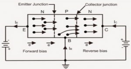
- As from above figure consider n-p-n transistor. The forward bias from base to emitter narrow’s the BE depletion region and the reverse bias from base to collector widens the BC depletion region shown in figure.
- The heavily doped N-TYPE emitter region is full with conduction band(frep) electron’s that easily diffuse through the forward biased BE junction into the p-type base region where they become minority carrier’s same as forward biased diode region
- The base region is lightly doped & very thin so that it has a very limited number of holes.
- Those only a small percentage of all the e-flowing the BE junction can combine with the available holes in the base.
- The relatively few recombined flow out of the base lead as valance electrons, forming as small base current.
- Most of the e flowing from the emitter into the thin lightly dooped base region do not recombine but diffuse into the BC depletion region.
- The BC depletion region diffuse e is being pulled across the reverse biased BC junction by the attraction of the collector supply vtg.
- The electrons now move through the collector region, out through the collector lead into the +ve terminal of the collector vtg source. This forms the collector electrons current.
- The collector current is much larger than the base current.
- This is the reason transistor exhibit current gain.
3.3.2 BJT Switching
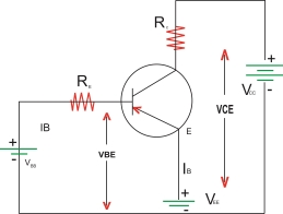
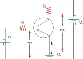
Common Emitter (CE) configuration
The important points about the CE
Configurations are as follows: the emitter acts as a common terminal between I/p and output. The /p Vtg. Is called between base and emitter
Hence VBE is the I/p Vtg. And IB is the input current.
The O/p is taken between the collector and emitter. There for VCE is the O/p Vtg. And IC is the O/p current.
In order to operate the transistor in its active region the base emitter (BE) junction is forward biased and collector base junction is reverse biased.
- Current relations in CE Configuration:
IE = IC + IB
Where IC =  d.c.IE + ICBO
Rearrange this eqn to get
IC – ICBO =  d.c.IE
 -
-  = IE = IC + IB
 ] = IB -
IC  ] = IB +
 ] +
] + 
- Current gain
 : as
: as  is the ration of o/p current TC and I/p current IB it called common emitter current amplification factor or simply current gain. Thus, transistor acts as current amplifier.
The value of  is match higher than
 =
= 
 =
=  =
=  =
= 
IC =  IB +
IB +  …….. I
But  =
= 
 1 +
1 +  =
=  + 1
+ 1
1 +  =
= 
 1 +
1 +  =
= 
Put in eqn I
IC =  IB + (1+
 ICBO above eqn can be expressed as
IC =  IB + ICEO
Where ICEO is the reverse saturation current for the CE configuration which is given by
ICEO = (1+  ) ICBO
- Reverse leakage current:
The Reverse leakage current of a transistor operating
In the LE configuration is denoted by
ICEO = (1 +  ) ICBO
As the value of 
- Match greater than 1 ICEO >>>> ICBO
- As IC =

Put IB = 0
 IC = (1 +
The Reverse leakage current (ICEO)
Increases with increase in the temperature this current flows in the same direction as that of IC there for the collector current IC will increase with increase in temperature even when IB is constant
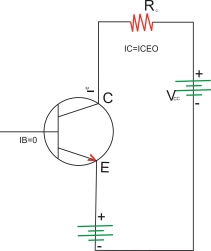
This is called as thermal instability so in CE configuration thermal stabilizing CKT must be included.
- Relation between IC and IB (Current gain
 )
)
We know that
IC 
Though ICEO is large it is much smaller as compared to . Therefor the eqn for IC gets modified as
 C =
C = 

- Relation betn
 &
& :
:
We know that
 but
but
 =
=  =
= 
 =
= 
Similarly we can obtain the expression for  d.c in terms of
  as follows
 d.c =
d.c =  but
but 
=
Multiply & divide numerator & denominator for by IE
 d.c =
d.c = 
 d.c =
d.c = 
 =
= 
- Impact characteristics:
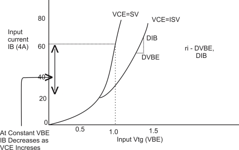
The value of dynamic input resistance ri is low for the CE configuration but it is not as low as that of CE configuration
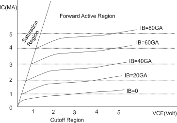
- Cutoff region: Both the BE & CB junctions are reverse biased to operate the transistor in cutoff region. The base current IB = 0 & the collector current is equal to the reverse leakage ICEO. The region below the characteristics for
IB = 0 is cutoff region.
- Active region: the BE emitter junction is forward biased CB junction is reverse biased to operate the transistor in the active region
The collector current IC increases slightly with increase in the vtg. VCE. However, the collector current is largely dependent on the base current IB
At fixed value of VCE if IB is increased then it will cause IC to increase substantially.
This is because IC = BIB this relation is true only for the active region of operation.
- Saturation region: the BE junction as well as the collector junction must be forward biased to operate the transistor in its saturation region
- Dynamic o/p resistance
 / constant IB
3.4.1 Common Base Characteristics
The notation and symbols of pnp and npn transistors are given below:
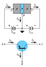
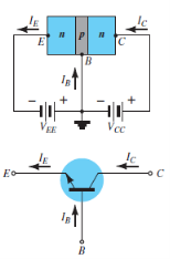
Fig. 4: PNP CB and NPN CB (Ref. 2)
Here the base is common to both the input and output sides of the configuration.
The flow of holes will govern the direction of current.
Hence, Ic = Ib + Ie
Where Ic, Ib, Ie are the collector, base and emitter currents respectively.
The graphical symbol of the PNP common base configuration is
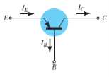
Fig.: PNP common base(Ref. 2)
The arrow in the above symbol shows the direction of emitter current in the device.
Now, to study the behavior of the device we require two characteristics:
Input Characteristic Curve
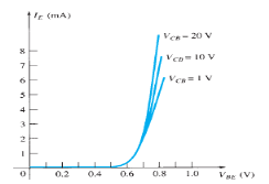
Fig.6: Input Characteristic Curve (Ref. 2)
- It is the relation between the input current IE to the input voltage VBE for various levels of output voltage VCB.
- It is also known as driving point characteristics.
Output Characteristic Curve
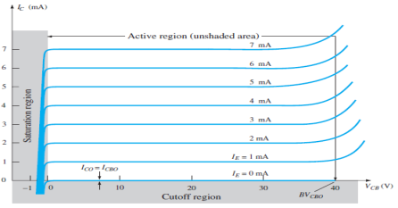
Fig.7 : Output Characteristic Curve (Ref. 2)
- It is the relation between the output current IC to the output voltage VCB for various levels of input current IE.
- It is also known as collector set of characteristics.
- It has three basic regions:
- Active Region
Here, base-emitter junction is forward biased and collector-base junction is reverse biased.
As input current IE increases above zero, output current IC increases to a magnitude equal to IE as determined by the basic transistor current relationship.
So, the first approximation determined by the curve is
IC ≈ IE
2. Cut-off Region
It is defined as the region where the collector current IC is equal to 0A.
Here, the base-emitter junction and the collector-base junction both are in reverse bias.
3. Saturation Region
It is the region that lies towards the left of VCB = 0V.
Here, the base-emitter junction and the collector-base junction both are in forward bias.
3.4.2 Common Emitter Characteristics
The notation and symbols of npn and pnp transistors are given below:
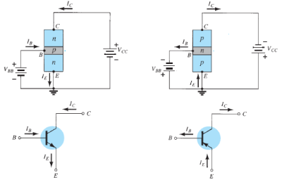
Fig.: NPN CE and PNP CE (Ref. 2)
In the above figure all the currents are shown in their actual conventional directions.
The current relation developed earlier is still applicable,
IE = IB + IC
Where IE , IB , IC are the collector, base and emitter currents respectively.
The graphical symbol of the PNP common emitter configuration is
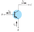
Fig.: PNP common emitter (Ref. 2)
Now, to study the behavior of the device we require two characteristics:
Input Characteristic Curve
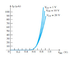
Fig.10: Input Characteristic Curve (Ref. 2)
It is the graph between the input current IB to the input voltage VBE for a range of values of output voltage VCE.
Note that the magnitude IB of is in micro amperes and that of IC is in milli amperes.
Output Characteristic Curve
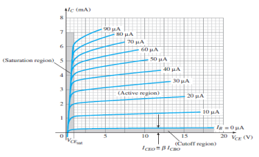
Fig.11: Output Characteristic Curve (Ref. 2)
It is the graph between the output current IC to the output voltage VCE for a range of values of input current IB.
It has three basic regions:
Active Region
- Here, the base-emitter junction is forward biased and collector base junction is reverse biased.
- These are the same conditions that existed in the active region of the common base configuration.
- This can be employed for voltage, current or power amplification.
Cut-off Region
- Here IC is not equal to zero when IB is zero.
- For linear amplification purposes, it is defined as IC = ICEO.
- The region below IB = 0µA is to be avoided for undistorted output signal.
- When the transistor is used as a switch, the condition should be ideally IC = 0mA for a chosen VCE voltage.
Saturation Region
- It is the region that lies towards the left of VCE = 0V.
3.4.3 Common Collector Characteristics
The notation and symbols of npn and pnp transistors are given below:
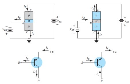
Fig. 12: NPN CC and PNP CC (Ref. 2)
In the above figure all the currents are shown in their actual conventional directions.
It is used for impedence matching purposes as it has high input impedence and low output impedence.
It can be designed using common emitter characteristics.
The output characteristics of common collector is same as that of common emitter configuration for all practical purposes.
The output characteristics are a plot between IE versus VCE for all values of IB.
The input current of common collector is same as that of common emitter configuration.
Here the region of operation will ensure that maximum ratings are not being exceeded and output ratings have minimum distortion.
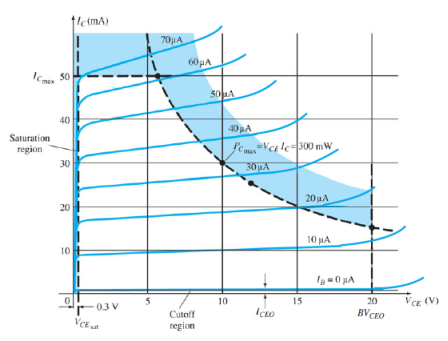
Fig.13: Output Characteristic Curve (Ref. 2)
The characteristics specifying the minimum VCE that can be applied without entering the non-linear region is saturation region.
The maximum power dissipation is given by,
P = VCE. IC
i) Take a multimeter and select its resistance range. We are taking NPN transistor here to understand the testing procedure.
Ii) The base of transistor is usually red connect it to the positive terminal of multimeter.
Iii) Connect negative terminal of multimeter to the collector of transistor. The collector is normally black in colour.
Iv) The multimeter should show open circuit.
v) Now let the base be connected to positive terminal of multimeter, connect emitter to the positive. It should show open circuit.
Vi) Connect negative terminal of multimeter to the base of transistor and connect collector to the positive and measure resistance. Then take it to the emmiter in both cases meter should deflect.
Vii) Connect neagative terminal of multimeter to collector and positive to the emitter. The meter should show open circuit.
Viii) Reverse the connections in step vii and again the meter should show open circuit.
Ix) If all the above steps show the correct results as mentioned the transistor is good, if not then its faulty.
3.6.1 Power Supply
It is an electronic instrument that supplies electric energy to the load. Its main task is to convert one form of electric energy to other. The regulated power supply means it supplies power to variety of output voltages for bench testing of electronic circuits, with variation of output voltages. Usually DC power source is used by electronic devices for operation. The regulated power supply consists of ordinary power supply and voltage regulating device. The voltage regulating device takes input from the ordinary power supply producing final output.
3.6.2 Function Generator
The function generator is an instrument which generates different types of wave form. The most required common wave forms are sine wave, saw tooth wave, triangle wave, square wave and these various outputs of the generator are available simultaneously. The purpose of providing simultaneously waves is fulfilled by the function generator In function generator the o/p waveform can be generated at a desired freqn in range from few hertz to several kilohertz. In the function generator the freqn is controlled which drives the integrator.The freqn controlled vtg is used to regulate two current source namely upper current source and lower current source. The upper current source supplies constant current to an integrator. The o/p vtg of integrator then increases linearly with time.If the current charging the capacitor increases or decreases the slope of o/p vtg increases or decreases respectively. Hence this controls freqn.
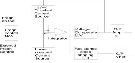
Block diagram of function generator
- The voltage comparator multi vibrator circuit changes the state of the n/w when the o/p vtg of integrator equals the maximum predetermined upper level.
- Because of this change in state the upper current source is removes and the lower current source is switched on
- This lower current source supplies opposite current to the integrator or ckt. The o/p of integrator decreases linearly with time when this o/p vtg equals maximum predetermine upper level on –ve side the comparator multi vibrator again changes the condition of the n/w by switching off the lower current source and switching on the upper current source
- The o/p vtg of the integrator has triangular wave form
- The freqn of this triangular wave form is determined by the upper current source and lower current source
- To get square wave the o/p of the integrator is passed through comparator.
- The vtg comparator delivers square wave o/p vtg of same freqn as that of i/p triangular wave form
- The sine wave is derived from triangular wave. The triangular wave is synthesised in to sine wave using diode resistance n/w in this shaper ckt , the slope of triangular wave is changed as it amplitude changes. This result in a sine wave with less than 1% distortion
- The two o/p amplifiers provide two simultaneous individually selected o/p of any of the wave form functions.
Application :
- It is used to generate different types of wave form simultaneous such as sine wave, square wave, triangular wave & saw tooth wave at a desired freqn from few hertz to several kilohertz.
- It is used to test bandwidth of audio freqnampɤ using square wave testing method
- It can be used in trouble shooting of various Analogas well as digital instruments.
- It is most extensively used as signal source for radio receiver alignment procedure.
3.6.3 CRO
They are generally used in laboratories. They are used to measure various waveforms. This device is very fast in plotting two dimensional characteristics. In this instrument a beam of electrons strikes a luminous screen and produce luminous spots. These spots move according to the variation of input variable.
Construction of CRO
The CRO consists of
1) Cathode ray tube: It is a vacuum tube which converts electrical signal into the visual signal. It has an electron gun and electrostatic deflection plates. A focused beam of electrons of high frequency is produced by electron gun. The electron beam is moved left to right by horizontal beam and vertical deflection plate moves the beam up and down.
2) Electronic gun assembly: This gun emits electron and form them into beam. It has heater, cathode, a grid, a focusing anode and an accelerating anode. There is a layer of barium and strontium to provide high emission of electrons at moderate temperature. The electron passes to control grid from the cathode grid. The CRO uses an electrostatic focusing tube.
3) Deflecting plate: The electron beam passes through two pair of deflecting plate after leaving the electron gun. The vertical deflecting plate produces vertical deflection and horizontal deflecting plate produces horizontal deflection.
4) Fluorescent Screen for CRT: The front of CRT is called face plate. It formed by shaping molten glass. The inner surface is coated with phosphor crystal which converts electric energy to light energy. When electron beam strikes the surface their energy level is raised and hence light is emitted.
5) Glass Envelop: It is conical shaped structure. There is aquadag coating between screen and inner surface of CRT. This surface is electrically connected to accelerating anode helping the electron beam to focus.
Working
The CRO figure is shown below. The electron is injected through control grid. This control grid has to control the light intensity of electron. The intensity of light depends on the negative potential of control grid. If the negative potential is low bright spot is produced and vice versa.
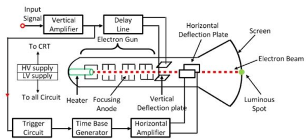
The electron beam further passes through focusing and accelerating anodes. These anodes being at high positive potential converge the beam to a point on screen. The beam than comes under the deflecting plates. The beam produces a spot when deflecting plate is at zero potential. The electron beam focuses upward when voltage is applied to vertical plate, and it is deflected horizontally when the voltage is applied to horizontal plate.
3.6.4 Multimeter
It is an electronic device used to measure voltage, current and resistance. It can also function as ohmmeter, voltmeter and ammeter. It has a needle over a numeric display for indication of the readings. It can be used to test continuity between two points in the circuit. The multimeter can be analog, digital and fluke multimeter.
Digital Multimeter :
- A Multi meter the most common measuring instrument. The name comes from multiple meter. There are two common types of Multi meter.
- The multimeter (DMMs) are the most common Measurement readings are displayed as numerical values on the LCD display. The display also alerts you to any pertinent symbols and warning.
- Digital meters on the other hand offer high accuracy have a high i/p impedance and are smaller in site.
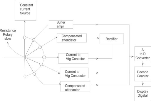
An instrument which is capable of measuring a.c. And d.c voltages a.c and d.c. Current and resistances over several range is called digital multimeter.The various measurement possible by DMM are resistance a.c voltage and current d.c voltage and current.The selection of the parameter is possible with the help of rotary switch connected to i/p probes of DMM.
- Resistance Measurement : The rotary switch is in position 1 and resistance is connected to input probes. The constant current source Drives a current through unknown resistance. This produces Vtg across resistance which is directly proportional to the resistance. It is given to the buffer amplify and then to analog to digital converter.The ADC converts it to equivalent digital signal and it is displayed with the help of digital display a.c voltage measurement : The rotary switch is in position 2 and i/p a.cvtg is applied to probes if it is above the selected range it is attenuated with the help of compensated attenuator It is rectified to produce proportional d.c vtg then it is given to ADC which display it in volts
- A.c current measurement : the rotary switch is in position 3 and unknown current is applied across i/p probes it is converted to proportional vtg using current to vtg convertors
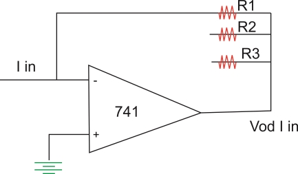
This I V converter is op-amp circuit as shown above. The op-amp/p current is zero hence I in flows through R1 and drop across R1osVo hence vtg o/p  the resistance R1 R2 and R3 are used for the proper range selection. This vtg is rectified and then given to ADC which sisplays the current in amperes.
3. D.c current measurement : The rotary switch is in position 4 and unknown d.c current is applied across i/p probes this vtg is given to ADC without rectification as this is proportional to d.c current ADC display it in amperes on digital display.
4. D.C voltage measurement : The rotary switch is in position 5 and unknown vtg is applied across i/p probes it is attenuated and directly given to ADC display it in volts.
Specifications of Digital Multimeter :
- D.C Voltage : this includes various d.c vtg ranges available along with the resolution and accuracy
- A.c Voltage : this includes various a.c vtg ranges available along with the resolution and accuracy.
- A.C current : this includes various a.c current ranges available along with the resolution and accuracy.
- Resistance : this includes the available resistance range typical six range are available from 200Ω to 20 MΩ the accuracy is
 0.1% of reading + two digits + 0.002Ω on the lowest range.
 - Input Impedance : The i/p Impedance is about 10 MΩ on all the range
- Normal mode noise rejection : this indicates the ability of the meter
It is greater than 60 dB at 50 HZ while the common mode noise rejection is greater than 90 dB at 50 HZ and greater than 120 dB at d.c
7. Overload protection : The overload protection of 1000 V d.c and 75 0ɤ.m.s. a.c is provided.
8. Diode test : The vtg drop across the diode can be measured for which 1 mA + 10% of constant current source is used.
9. Conductance : It can display Conductance in siemens
10. Relative Reference : when RF1 button is pressed the displayed reading is stored as a reference and then subtracted from the subsequent readings to indicate only amount of deviation from the reference.
11. Frequency : The frequency ranges is 200HZ to 200 kHZ auto selection.
References:
1. David A Bell, Electronic Devices and Circuits Oxford Higher Education, 5th Edition,
(2017).
2. NN Bhargava, DC Kulshreshtha, SC Gupta, Basic Electronics and Linear circuits,
Tata McGrawHill Publishing Company, 2nd Edition, (2013).