Unit – 5
Digital-to-Analog converters
In the weighted resistor type DAC, each digital level is converted into an equivalent analog voltage or current.
The following figure is the binary weighted resistor type DAC.
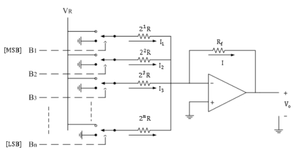
Fig.1: Weighted resistor
Here 
It consists of parallel binary weighted resistor bank and a feedback resistor Rf.
The switch positions decide the binary word (i.e.B1B2B3…Bn).
Here, op-amp is used as current to voltage converter.
Disadvantages:
1) When number of binary input increases, it is not easy to maintain the resistance ratio.
2) Very wide ranges of different values of resistors are required.
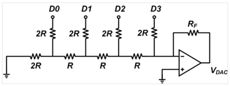
Circuit Operation
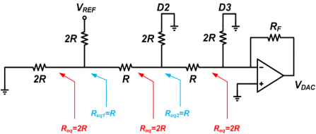
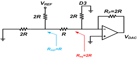
Assume that D0 is connected to VREF and the other bits are logic low
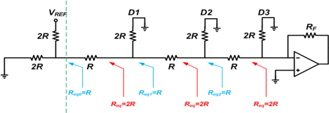
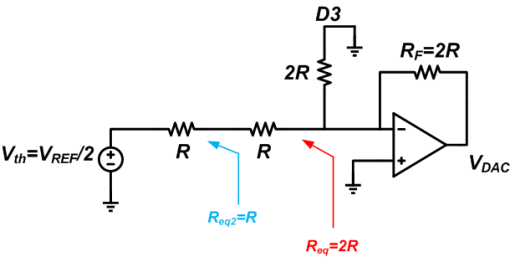
Applying the Thevenin theorem

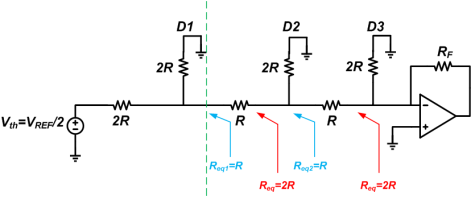

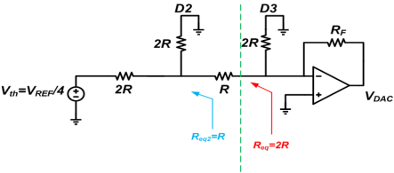
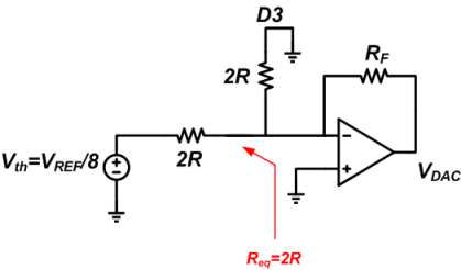
Assuming RF=2R, the output voltage will be VDAC = -2R ✖ (VREF/8)/2R = -VREF/8.
This output voltage corresponds to the DAC LSB.
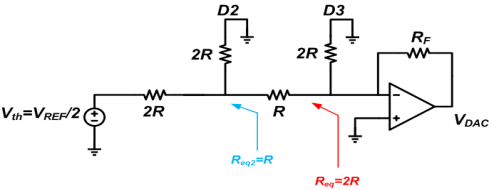
Here, the input is VREF/2 instead of VREF/4. Considering the result of the case D3D2D1D0 = 0001, if RF = 2R we obtain VDAC = -VREF/4.
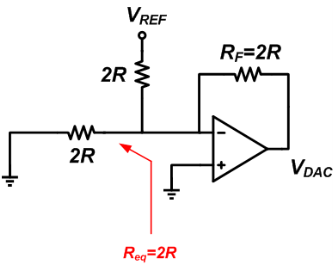
The output voltage will be VDAC = -(VREF/2R) ✕2R = -VREF.
It is an N-bit version of this DAC simply consists of 2N equal resistors in series and 2N switches (usually CMOS), one between each node of the chain The simplest DAC structure of all, after the changeover switch mentioned above, is the Kelvin divider or string DAC as shown in Figure. An N-bit version of this DAC simply consists of 2N equal resistors in series and 2N switches (usually CMOS), one between each node of the chain.
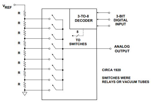
This architecture is simple, has a voltage output (but a code-dependent output impedance) and is inherently monotonic—even if a resistor is accidentally short-circuited, output n cannot exceed output n + 1.
It is linear if all the resistors are equal, but may be made deliberately nonlinear if a nonlinear DAC is required. Since only two switches operate during a transition, it is a low-glitch architecture. Also, the switching glitch is not code-dependent, making it ideal for low distortion applications. Because the glitch is relatively constant regardless of the code transition, the frequency content of the glitch is at the DAC update rate and its harmonics—not at the harmonics of the fundamental DAC output frequency.
The major drawback of the string DAC is the large number of resistors and switches required for high resolution, and as a result it was not commonly used as a simple DAC architecture until the recent advent of very small IC feature sizes made it very practical for low and medium resolution DACs. Today the architecture is quite widely used in simple DACs, such as digital potentiometers and, as we shall see later, its current output version, the thermometer DAC, is also used as a component in more complex high resolution segmented DAC structures. The output of a DAC for an all "1"s code is 1 LSB below the reference, so a string DAC intended for use as a general-purpose DAC has a resistor between the reference terminal and the first switch
The simplest form of an integrating ADC uses a single-slope architecture (Figures a and b). Here, an unknown input voltage is integrated and the value compared against a known reference value. The time it takes for the integrator to trip the comparator is proportional to the unknown voltage (TINT/VIN). In this case, the known reference voltage must be stable and accurate to guarantee the accuracy of the measurement.
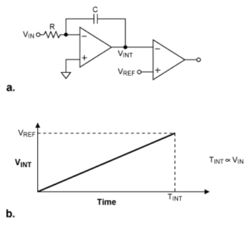
One drawback to this approach is that the accuracy is also dependent on the tolerances of the integrator's R and C values. Thus, in a production environment, slight differences in each component's value change the conversion result and make measurement repeatability quite difficult to attain. To overcome this sensitivity to the component values, the dual-slope integrating architecture is used.
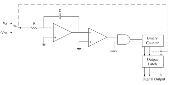
In dual slope type ADC, the integrator generates two different ramps, one with the known analog input voltage VA and another with a known reference voltage –Vref. Hence it is called a s dual slope A to D converter. The logic diagram for the same is shown below.
Operation:
The binary counter is initially reset to 0000; the output of integrator reset to 0V and the input to the ramp generator or integrator is switched to the unknown analog input voltage VA.
The analog input voltage VA is integrated by the inverting integrator and generates a negative ramp output. The output of comparator is positive and the clock is passed through the AND gate. This results in counting up of the binary counter.
The negative ramp continues for a fixed time period t1, which is determined by a count detector for the time period t1. At the end of the fixed time period t1, the ramp output of integrator is given by
∴VS=-VA/RC×t1
When the counter reaches the fixed count at time period t1, the binary counter resets to 0000 and switches the integrator input to a negative reference voltage –Vref.
Now the ramp generator starts with the initial value –Vs and increases in positive direction until it reaches 0V and the counter gets advanced. When Vs reaches 0V, comparator output becomes negative (i.e., logic 0) and the AND gate is deactivated. Hence no further clock is applied through AND gate. Now, the conversion cycle is said to be completed and the positive ramp voltage is given by
∴VS=Vref/RC×t2
Where Vref & RC are constants and time period t2 is variable.
The dual ramp output waveform is shown below.
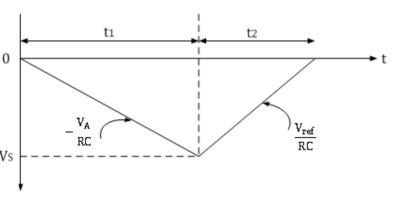
Since ramp generator voltage starts at 0V, decreasing down to –Vs and then increasing up to 0V, the amplitude of negative and positive ramp voltages can be equated as follows.
∴Vref/RC×t2=-VA/RC×t1
∴t2=-t1×VA/Vref
∴VA=-Vref×t1/t2
Thus, the unknown analog input voltage VA is proportional to the time period t2, because Vref is a known reference voltage and t1 is the predetermined time period.
The actual conversion of analog voltage VA into a digital count occurs during time t2. The binary counter gives corresponding digital value for time period t2. The clock is connected to the counter at the beginning of t2 and is disconnected at the end of t2. Thus, the counter counts digital output as
Digital Output=(counts/sec) t2
∴Digital output=(counts/sec) [t1×VA/Vref]
For example, consider the clock frequency is 1 MHz, the reference voltage is -1V, the fixed time period t1 is 1ms and the RC time constant is also 1 ms. Assuming the unknown analog input voltage amplitude as VA = 5V, during the fixed time period t1, the integrator output Vs is
∴VS=-VA/RC×t1= (-5)/1ms×1ms=-5V
During the time period t2, ramp generator will integrate all the way back to 0V.
∴t2=VS/Vref ×RC= (-5)/ (-1) ×1ms=5ms=5000μs
Hence the 4-bit counter value is 5000, and by activating the decimal point of MSD seven segment displays, the display can directly read as 5V.
- Successive Approximation type ADC is the most widely used and popular ADC method.
- The conversion time is maintained constant in successive approximation type ADC, and is proportional to the number of bits in the digital output, unlike the counter1and continuous type A/D converters.
- The basic principle is that the unknown analog input voltage is approximated against an n-bit digital value by trying one bit at a time, starting with the MSB.
- It operates by successively dividing the voltage range by half.
(1) The MSB is initially set to 1 with the remaining three bits set as 000. The digital equivalent voltage is compared with the unknown analog input voltage.
(2) If the analog input voltage is higher than the digital equivalent voltage, the MSB is retained as 1 and the second MSB is set to 1
Example:
Let us assume that the 4-bit ADC is used and the analog input voltage is VA = 10V. When the conversion starts, the MSB bit is set to 1.
Now VA = 10V > VD = 8V = [1000]2
Since the unknown analog input voltage VA is higher than the equivalent digital voltage VD, as discussed in step (2), the MSB is retained as 1 and the next MSB bit is set to 1 as follows
VD = 12V = [1100]2
Now VA = 11V < VD = 12V = [1100]2
Here now, the unknown analog input voltage VA is lower than the equivalent digital voltage VD. As discussed in step (2), the second MSB is set to 0 and next MSB set to 1 as
VD = 10V = [1010]2
Now again VA = 9V > VD = 9V = [1001]2
Again as discussed in step (2) VA>VD, hence the third MSB is retained to 1 and the last bit is set to 1. The new code word is
VD = 10V = [1010]2
Now finally VA = VD, and the conversion stops.
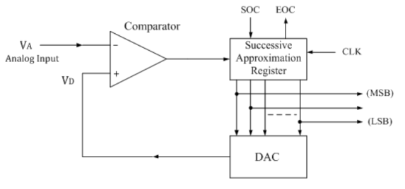
It consists of a successive approximation register (SAR), DAC and comparator. The output of SAR is given to n-bit DAC. The equivalent analog output voltage of DAC, VD is applied to the non-inverting input of the comparator. The second input to the comparator is the unknown analog input voltage VA. The output of the comparator is used to activate the successive approximation logic of SAR.
When the start command is applied, the SAR sets the MSB to logic 1 and other bits are made logic 0, so that the trial code becomes 1000.
Advantages:
- Conversion time is less.
- Conversion time is constant and independent of the amplitude of the analog input signal.
Disadvantages:
- Circuit is complex.
- The conversion time is more.
A flash type ADC produces an equivalent digital output for a corresponding analog input in no time. Hence, flash type ADC is the fastest ADC.
The 3-bit flash type ADC consists of a voltage divider network, 7 comparators and a priority encoder.
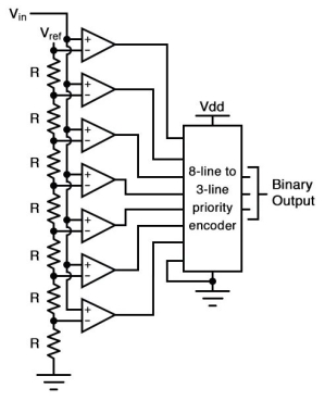
Fig. Circuit diagram of a 3-bit flash type ADC
The working of a 3-bit flash type ADC is as follows.
- The voltage divider network contains 8 equal resistors. A reference voltage VRVR is applied across that entire network with respect to the ground. The voltage drop across each resistor from bottom to top with respect to ground will be the integer multiples (from 1 to 8) of VR8VR8.
- The external input voltage Vi is applied to the non-inverting terminal of all comparators. The voltage drop across each resistor from bottom to top with respect to ground is applied to the inverting terminal of comparators from bottom to top.
- At a time, all the comparators compare the external input voltage with the voltage drops present at the respective other input terminal. That means, the comparison operations take place by each comparator parallelly.
- The output of the comparator will be ‘1’ as long as Vi is greater than the voltage drop present at the respective other input terminal. Similarly, the output of comparator will be ‘0’, when, Vi is less than or equal to the voltage drop present at the respective other input terminal.
- All the outputs of comparators are connected as the inputs of priority encoder. This priority encoder produces a binary code (digital output), which is corresponding to the high priority input that has ‘1’.
- Therefore, the output of priority encoder is nothing but the binary equivalent (digital output) of external analog input voltage, Vi
The flash type ADC is used in the applications where the conversion speed of analog input into digital data should be very high.
A switched capacitor (SC) is an electronic circuit element implementing a filter. It works by moving charges into and out of capacitors when switches are opened and closed. Usually, non-overlapping signals are used to control the switches, so that not all switches are closed simultaneously.
Capacitor circuit configurations
Capacitive voltage divider
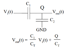
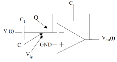
Capacitive Feedback

Multiple input voltage divider
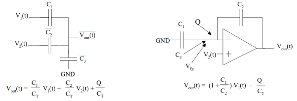
Integrator:
The op-amp integrator is the most frequently chosen building block for switched-capacitor filters. The standard RC integrator is shown in Figure.

Figure. Standard op-amp integrator, with transfer curve
To review, the voltage transfer function of this circuit is given by

Where  . Now, if one replaces the resistor by its switched-capacitor equivalent, as shown in Figure 3b, and use Eq. 1 as the resistor's value, one finds


Figure. Switched-capacitor integrator.
Again, one notes the fact that this new integrator has no resistors, which take up excessive silicon die area. Also, the -3 dB frequency, f0, depends on a ratio of capacitances, not on an RC product. The tolerances for ratios are much easier to control than the tolerances for products. Finally, this characteristic frequency of the integrator is inherently settable with a simple change in the clock frequency.
The typical values of capacitances used in switched-capacitor technology range from 0.1 pF to 100 pF. These are low enough values that the stray capacitances of the MOS switches, of the interconnects, and of the "plates" of the switched-capacitors themselves can all have a significant effect on the desired frequency response of the filters designed with switched-capacitors. The effects of stray capacitance have been reduced greatly by dual-switch configurations [2, 7]. Figure shows explicitly the clock phasing of the MOS switches which acts to eliminate the transient charge transfer through the stray capacitances, Cs1 and Cs2, also indicated in the figure. In essence, charge transfer only takes place through the capacitor C1. Figures 5a and 5b show both the inverting and noninverting stray-insensitive integrator. The noninverting stray-insensitive integrator is obtained simply by switching the clock phasing on transistors M2 and M4.
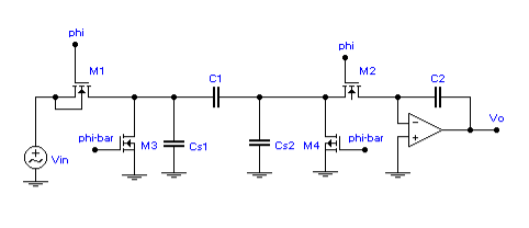
Figure. Arrangement of extra MOSFET's and clock signals to make switched capacitor circuit insensitive to stray capacitances.
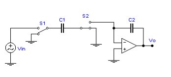
Figure. Switch setting used to realize stray-insensitive inverting integrator.

Figure. Switch setting for stray-insensitive non-inverting integrator.
Because of the importance of the integrator to switched-capacitor filters, it is necessary to be familiar with the variants of the integrator. These include the summing integrator, the differential integrator, the integrator/summer, and the lossy integrator. All of these play a role in the synthesis of switched-capacitor filters. The summing integrator, shown below in Figure 6, has a response given by:

Where  and
and  are
are


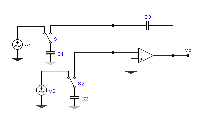
Figure. Summing integrator.
The easiest way to understand this circuit is to look at what happens to the charge accumulation on the capacitor C1 when the switches are thrown to the left. In this case, the capacitor charges up to a value of V1 – V2. When the switches are thrown to the right, the charge on the capacitor is poured into the op-amp's summing node. The average current, assuming the switching rate (= clock frequency) is high enough, is given by

This results in a stray-insensitive output voltage of


Where 

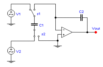
Figure. Differential integrator.
The lossy integrator provides a simple, first-order lowpass response with gain. This circuit is realized by placing a switched-capacitor (i.e., a simulated resistor) in parallel with a feedback capacitor, Figure 8. In general, the easiest way to analyze the response of more complex switched-capacitor circuits such as this one is to replace all switched-capacitors with their resistor equivalents. Once the transfer function is found for a circuit with resistors (and discrete capacitors), then the switched-capacitor equivalents of the resistors (Eq. 1) can be placed back in the transfer function to obtain the final result. For the lossy integrator, the analysis proceeds as follows:


Where the "0" in  and in
  refers to the virtual ground at the op-amp's inverting input. The transfer function is obtained using these resistor equivalents:


Now substituting the switched-capacitor equivalents for the resistors, one obtains

Where  is the critical, or -3 dB, frequency of the lowpass filter. Eq. 8 has the form of a lowpass filter multiplied by a gain proportional to the ratio of the two switched-capacitors.
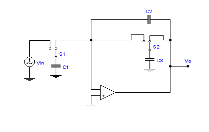
Figure. Lossy integrator, or first-order lowpass filter with gain.
Amplifier:
Although the initial impetus for the development of the switched-capacitor was the opportunity and need to synthesize active filters that would be compatible with MOSFET technology, the early 1980's found many other uses for the switched-capacitor. Linear Technology has developed the LTC1043 [9], which contains dual switched capacitor networks, along with an on-chip non-overlapping clock generator, oscillator, and charge balancing circuitry.
The clock generator controls both of the switch networks, while the charge balancing circuitry is designed to cancel any effects due to stray capacitance. The on-chip oscillator has a fixed frequency of 185 kHz. An external capacitor can be connected across pins 16 and 17 (for the instrumentation amplifier) to yield any desired clock rate. The desired clock rate can be found from
 ; the 24-picofarad capacitance is the internal capacitance responsible for the oscillator’s fixed frequency.
Among the circuits developed from the LTC1043 are instrumentation amplifiers, lock-in amplifiers for detecting extremely small parameter shifts in sensor applications, and signal conditioners for platinum resistance temperature detectors (RTD), relative humidity sensors, and LVDT’s. The instrumentation amplifier is a standard op-amp circuit presented in many electronics texts [5-6], and is designed to amplify small difference signals such as might be found in measurement or transducer applications. At the same time, common-mode or noise signals picked up by the lines feeding the amplifier must be suppressed, especially as these signal levels are often larger in amplitude than the sought-for difference signals. Figure 13 shows the LTC1043 combined with a standard non-inverting op-amp to give an instrumentation amplifier with a common-mode rejection ratio (CMRR) of >120 dB. Figure shows the same circuit with the ½ LTC1043 as a black box.
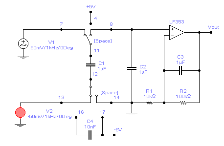
Figure. Instrumentation amplifier using ½ of LTC 1043 switched-capacitor, along with LF356/353 op-amp in non-inverting configuration.
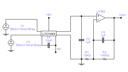
Figure. Switched-capacitor-based instrumentation amplifier, with ½ LTC1043 shown as a black box. The pin numbers in Figure 13 are the pins in the black box in this figure.
Operation:
First, the dual switch, when flipped to the left, charges the capacitor C1 up to the difference V1 – V2.
Second, on the next clock pulse, the switches will then dump the charge represented by that voltage difference onto C2.
Third, the continuous clocking from the oscillator will force C2 to eventually develop a voltage equal to the difference voltage.
Finally, the difference voltage, with the common-mode signal stripped off by the LTC1043 is amplified by the op-amp.
It is interesting to observe several features of this circuit and compare them to the standard instrumentation amplifier. By using the capacitor C1 (the so-called “flying capacitor”), the common-mode voltage present at the inputs is looking into a capacitive voltage divider, between the C1 and the LTC1043’s parasitic capacitance.
This parasitic capacitance is typically less than 1 picofarad, so the AC value of the CMRR is > 120 dB. By comparison, Analog Device’s AD624 instrumentation amplifier can go as high as 130 dB for high gains, up to 60 Hz. Because of the capacitive voltage divider from the LTC1043, this instrumentation amplifier shows higher CMRR, over a wider range of voltage gains, and to a higher frequency.
References:
1. R. P. Jain, "Modern Digital Electronics", McGraw Hill Education, 2009.
2. M. M. Mano, "Digital logic and Computer design", Pearson Education India, 2016.
3. A. Kumar, "Fundamentals of Digital Circuits", Prentice Hall India, 2016.