Module-1
Atomic and Molecular Structure
The molecular orbital theory of diatomic molecule can be considered as by taking the H2 molecule in consideration. The molecular orbital are made up of symmetric (both the hydrogen atom are stretched toward the same side) or asymmetric (both the hydrogen atom are stretched toward the opposite side) combination of the 2 atoms to their 1s atomic orbital. According to Molecular Orbital Theory the 1s orbital combine together to form the 2 new molecular orbital of the same Hydrogen molecule with one of it having a lower energy state than the 1s orbital. This MO is denoted by (Sigma1s and Sigma*1s). The molecular orbital with higher energy are called as bonding molecular orbital while the other orbital is anti-bonding molecular orbital.
MO Energy level Diagram for Homonuclear Diatomic molecules:
H2 molecule
H2 molecule consist of two H atoms and their two electrons. Two 1s orbitals give two MOs- one bonding that is σ and another one is antibonding that is σ*. The bonding orbital is in lower in energy state, the two electron occupies the bonding MO. The MO electron configuration of H2 molecule is written as (σ1s) 2.
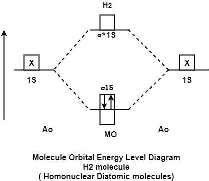
Energy evolved =
[No. of electron in BMO (-) + No. of electron in Anti Bonding Molecular Orbital * (+)]
=2*(- ) + 0*(+ )
= -2
This evolved energy is called as stabilization energy.
The molecule is stable so it is diamagnetic.
MO Energy level Diagram for Heteronuclear Diatomic molecules:
Carbon Monoxide Molecule (CO)
CO is the hetronuclear diatomic molecule. This molecule is formed by the combination of carbon and oxygen atom. Electronic configuration of carbon atom is 1s2, 2s2, 2p2 and that of oxygen is 1s2, 2s2, 2p4
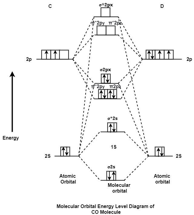
Stabilization Energy
[No. of electron in BMO * (-) + No. of electrons in anti bonding molecular orbital * (+)]
=(8) * (-) + (2) * (+)
= -6
This is extracted from the X-ray diffractions that solid is an ordered structure therefore the atoms of solids interact strongly and setup an internal electric field that is periodic in nature. This periodic electric field affects the motion of free electrons. The application of quantum mechanics to the motion of electrons in solids shows that the allowed value of electron energy is distributed in bands. The most fundamental unit of matter which is capable of independent existence is called atoms. The atoms consist of center body which is called as the nucleus while it is surrounded by the electrons. The electrons present at the outermost orbits are called valence electrons. Each atom has different orbits and hence all of it is having the different energy levels. These energy level consist of several quantum states. The atoms are grouped together to form the solids which consist of millions of electron belonging to each orbit of atoms. Each of them possessing the different energy. As long as the atoms are separated their interaction are negligible. As atoms comes together to create a closed pact periodic structure they interact strongly due to their proximity to each other. This tends to leave behind the state of energy level is same for all an isolated atoms there arise closely state separate levels which falls into groups. The transformation of single energy level into 2 or more separate energy level is energy level splitting. When 2 atoms come close then 1 energy level split in 2 energy level and so on. In general an interacting atoms cause a particular energy level split into n level. The group of discrete and closely space energy levels resulting from splitting is called as the energy bands.
Liquid Crystals: There are three state of matter i.e.; Solid, Liquid, Gas. Liquid Crystal is the fourth state that enters under the right conditions and consequences. The matter which shows the property between the conventional Liquid and Solid Crystals. This can be simplified in this manner that the Liquid Crystals may flow like the liquid but the molecule of the crystal may be in the crystal form. The molecules in the liquid crystal do not exhibit any positional order instead they represent the orientational order. They tend to orient in one direction more than other hence this direction is known as the director of the Liquid Crystals.
There are several phases in Liquid Crystal.
1-Mesomorphic Phases
1.1-Thermotropic Liquid Crystal
1.2-Lyotropic Liquid Crystal
Thermotropic Liquid Crystal class can be prepared by heating. The known crystals are organic compounds. Ex.- bis-(p-methylbenzal)-p.
While at another end the Lyotropic Liquid Crystal are prepared by the mixture of two or more components.
Applications
Liquid Crystal Display:
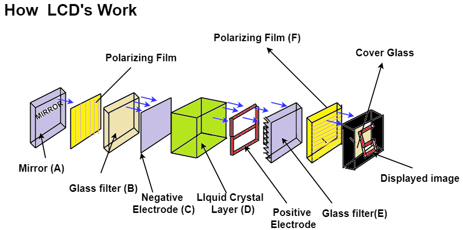
Polarization: Light wave is an electromagnetic wave in which time barring electric field vector E bar and magnetic field vector V bar are mutually perpendicular to each other and perpendicular to the direction of propagation of light wave. In a light wave electric field vector vibration occurs in different planes such light wave are unpolarised light wave. If it is confined in particular direction then such light wave is polarized light wave. This phenomenon is called Polarization. When unpolarised light pass through the polarizer then the vibration of polarizer tend to polarize the light. While in Liquid Crystal Display the intensity of light can be controlled at a given point by changing the orientation of molecules. The optical properties of the liquid crystal can often are manipulated by subjecting it to a magnetic or electric field that changes the orientation of the molecules. The number of regions or the pixels in there per unit area responsible for the following conditions:
Very low Resolution
Low Resolution
Improved Resolution
High Resolution
Working of Liquid Crystal Display:
It is based on change in optical properties of LCD which is caused by electric fields. In LCD the thin film of Liquid Crystal usually the Nematic crystal is sandwich in between thin transparent electrodes. The arrangement is provided to apply an electric field across a small area of this thin film usually called as pixel. This is used to apply electric field across a small area of this thin film of liquid crystal. TFT Matrix means thin film transistor matrix. This is the arrangement which provide electric field to the small region of this liquid crystal film on both side of transparent electrode polarized filter is placed. One polarizing filter placed between backlight and the LC films while another one is placed between liquid crystal film and screen. The white light is meant to pass through the filter then after that this light fall on Liquid Crystal film the liquid crystal changes the polarization of light and this change is controlled by applying electric field to various point on the Liquid Crystal film. This electric field is applied at various point which are called as Pixels with help of TFT matrix, change in polarization lead to change in intensity of light at different points. The combine effect of change in intensity at all the point form the image which can be seen at the screen. Eg.Computer Screen, Watches etc.
Perfect Crystal: A perfect crystal is that crystal in which atoms are arranged in that manner that atoms possess equal numbers of positive ions as well as the negative ions hence systematical manner, geometrical manner arrangement of the ions without any defects are called as perfect crystal. This perfectness of a crystal explains many properties of crystal like magnetic property of crystal etc. While it does not explain the density or color.
Defects mean deviation which are localized in the crystal. The deviation under the perfect arrangement of the crystals is called as the defects. On that basis the there are so many type of defect can be seen like as Line Defect, Color Defect, Point Defects.
Point Defects: Deviation are to localized in the atom due to its neighboring atom or its surrounding atoms is called as Point Defects. This can classify in following ways:
Impurity Defect: This is also called as manufacturing defect as because at the time some foreign atoms replace some of the atoms from the original lattice
Substitutional Defect: Substitutional Defect is that defect in which the impurity atoms substituted existing atom of the Original Lattice by overlapping the existing atom and tend to provide the defect in the crystal. This defect is called as the Substitutional Defect.
Interstitial Defect: Interstitial Defect is that defect in which the impurity atoms enter into the Original Lattice and occupy the vacant space left after the complete creation of the Lattice.
Vacancy Defect: The missing up of an atom from its original lattice site after the manufacturing up of the crystal is called vacancy defects. Vacancy defect create the empty lattice site. As due to the loss of atom the neighboring atoms get under the tension in the crystalline solids. It tends to result in the reduction in the density of the solids, which in result increase the hardness of the solids.
Schottkey: This defect comes in known in the name of scientist Walter H. Schottkey. In his model he explains about the loss of Ions from the original lattice. There would be the equal loss of the positive and negative ions from the lattice to maintain the neutrality of the lattice. Hence this defect is called Schottkey Vacant defect.
Frenkel Defect: This defect comes in known in the name of scientist Yakov Frenkel. Either cation or anion leaves its site and move to the unfilled volume and dissolve the interstitial of the lattice.
Graphite:
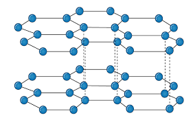
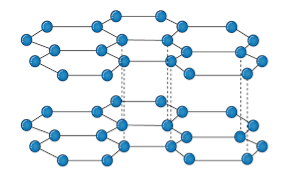
It is an allotropic form of the carbon atom (Allotropy form- When any element is formed in more than one form and in each form they posses different property). In graphite carbon are arranged in hexagonal ring form and each form is arranged upside down to form the layer and are attached together by weak Vander-wall’s forces. Graphite is the most stable form of the carbon. It is the good conductor of heat and electricity. The two major known form of graphite are alpha (Hexagonal) and Beta (Rhombohederal).
Structure:
The carbon atom is sp2 hybridized that means there is 4 valence electron in their outermost shell as in the diamond the all 4 valence electron are covalently bonded while in graphite the 3 electron makes a covalent bond while the remaining 1 electron are free. The interconnection of these carbon atoms forms the hexagonal structure. The C-C bond bond length is 1.42 Angstrom. This hexagonal layer attached toward each other by weak Vander Wall forces at a distance of 3.35 Angstrom. This is the reason why graphite is soft.
Properties:
Conducting Property: As the carbon of Graphite are sp2 hybridized that means the p orbital remain vacant of the carbon atom this tend to overlapping of the vacant P-orbital. This overlapping of the vacant orbital is responsible for the movement of electrons in parallel on their vacant orbital that is why Graphite shows the conducting property.
Lubricating Property: There is presence of weak Vander Wall forces between two layers due to these weak forces the two layers are flexible in nature which in result make the Graphite to be used for Lubricating purpose.
Applications:
1-Graphite can be used as the solid lubricant
2-Graphite can be used as conductor.
3-Graphite can be used as the electrodes.
Fullerenes:
It is an allotropic form of the carbon atom (Allotropy form- When any element is formed in more than one form and in each form they posses different property). An Er. & Scientist Richard Buckminster Fuller extracted that carbon is having cluster the very first form gathered is C16.
Structure:
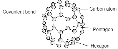
Fullerene is a soccer ball like structure which is hollow from inside and is polymorphic in nature (arrange in hexagon and pentagon form) These are arranged in manner that posses 2 hexagon share a common wall while 2 different pentagon never share the common wall. Each carbon atom is sp2 hybridized. Electric spark is produced at graphite ectrode at inert atmosphere and low pressure which gives back black soot that consist of fullerene and impurities. These impurities are removed by the method of sublimation.
Properties:
All carbon atoms are sp2 hybridized with FCC in nature. This is mustard yellow in color. The fullerene may be Exohederal or Endohederal structure based on the occupying the space.
Applications:
1-Used as super conductors
2-Fulleren is used in making the Ferro magnets
3-It can be used for making non-linear electronic devices.
The designing and making up of anything whose use depends on the specific structure at nanoscale. These posses the different properties at reducing scale. The measurement can be taken in notice at 100 nanometers and lesser is called as the nanotechnology. This includes the materials made by the manipulation of up of atoms or molecules. They are composed up of metals, ceramics, polymers, organic materials in simpler way these all are made up of carbon compounds. The technology that we deal with in taking the consideration up of the Nanomaterial is called as the nanotechnology.
Applications:
1- Nanomaterial will be used as the next generation computer chips.
2- Nanomaterial will be responsible for the High Definition TV.
3- Branch deals in reducing the cost of the flat panel displays.
4- Nanotechnology plays a major role in improving the density of the battery.
5- Nanotechnology contributes in the changing trends by playing the major role in improving the sensivity of the sensors.
References:
1. University Chemistry By B.H. Mahan
2. University Chemistry By C.N.R. Rao
3. Organic Chemistry By I.L. Finar
4. Physical Chemistry By S. Glasstone
5. Engineering Chemistry By S.S. Dara
6. Polymer Chemistry ByFre W., Billmeyer
7. Engineering ChemistryBy Satya Prakash