Unit-2
Bipolar Junction Transistor
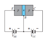
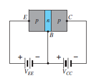
Fig 1 : (a) pnp transistor (b) npn transistor
Basic theory and operation of PNP and NPN transistors:
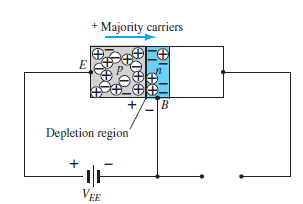
Fig. 2: Forward bias of pnp transistor (Ref. 2)
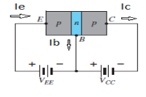
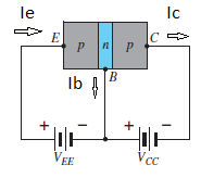
Fig. 3: pnp transistor (Ref. 2)
Ie = Ic + Ib
Ic = Icm + Ico
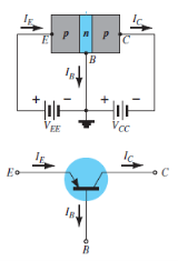
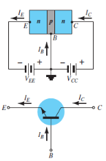
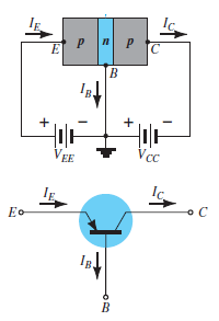
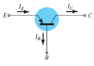
Fig. 4: PNP CB and NPN CB (Ref. 2)
Where Ic, Ib, Ie are the collector, base and emitter currents respectively.
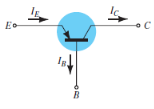
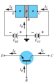
Fig. 5 : PNP common base(Ref. 2)
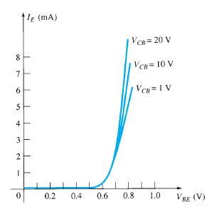
Input Characteristic Curve
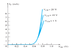
Fig.6: Input Characteristic Curve (Ref. 2)
Output Characteristic Curve
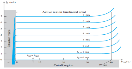
Fig.7 : Output Characteristic Curve (Ref. 2)
IC ≈ IE
2. Cut-off Region
3. Saturation Region
Common Emitter Configuration
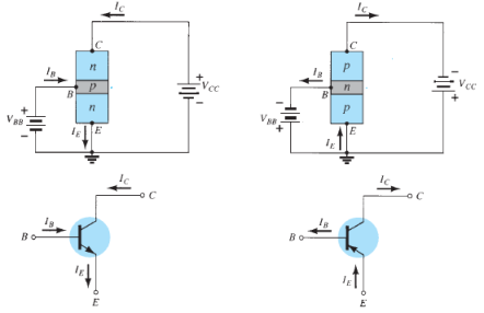
Fig. 8: NPN CE and PNP CE (Ref. 2)
IE = IB + IC
Where IE , IB , IC are the collector, base and emitter currents respectively.
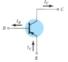
Fig. 9 : PNP common emitter (Ref. 2)
Input Characteristic Curve
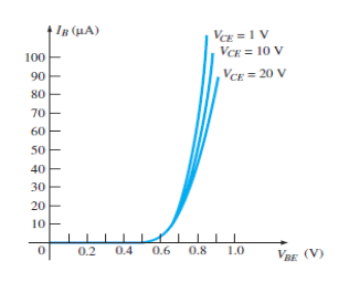
Fig.10: Input Characteristic Curve (Ref. 2)
Output Characteristic Curve
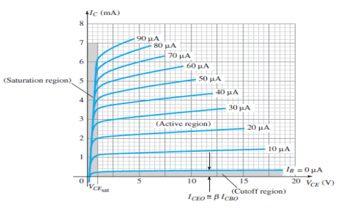
Fig.11: Output Characteristic Curve (Ref. 2)
Active Region
Cut-off Region
Saturation Region
Common Collector Configuration
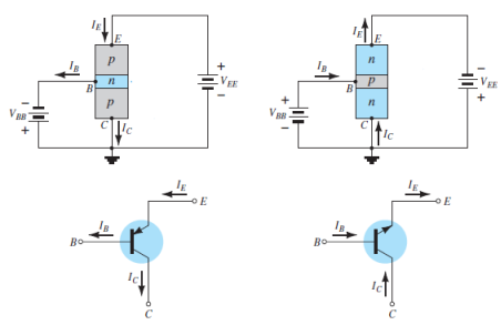
Fig. 12: NPN CC and PNP CC (Ref. 2)
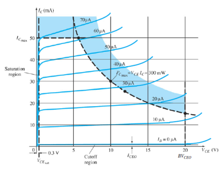
Fig.13: Output Characteristic Curve (Ref. 2)
P = VCE . IC
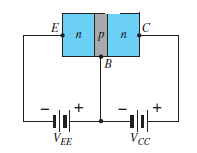
Fig.14: FET
Operation
I-V characteristics
Output Characteristics or Drain Characteristics
2. With external bias: When the external bias is applied to the gate-source terminal, the gate-source terminal becomes reversed bias externally. Obviously, if we are supplying an external voltage, then we can achieve the pinch-off point quite early as compared to the circuit which is not biased.
Transfer Characteristics
The transfer characteristics can be determined by observing different values of drain current with variation in gate-source voltage provided that the drain-source voltage should be constant. The transfer characteristics are just opposite to drain characteristics.
Characteristic
The MOSFET (Metal Oxide Semiconductor Field Effect Transistor) transistor is a semiconductor device which is widely used for switching and amplifying electronic signals in the electronic devices.
It is a core of integrated circuit and is designed and fabricated in a single chip because of its small size.
It is a four-terminal device with source(S), gate (G), drain (D) and body (B) terminals.
The body of the MOSFET is connected to the source hence making it a three-terminal device like field effect transistor. It can be used in both analog and digital circuits.
Operation
Function:
When there is no voltage on the gate, the channel shows maximum conductance. When the voltage on the gate is either positive or negative, the channel conductivity decreases.
2. Enhancement Mode
The device does not conduct when there is no voltage on the gate. As the voltage increases on the gate, the better the device can conduct.
Working:

References:
1 “Electronic devices and circuit theory” by Boylestead and Nashelsky, Pearson
2 “Electronic principle” by Albert Malvino and Davis J Bates, TMH
3 “Integrated Electronics”, By Jacob Millman and Christos Halkias


