Unit-4
Digital Electronics
A digital system understands positional number system where there are few symbols called digits and this symbol represents different values depending on their position in the number.
A value of the digit is determined by using
Decimal Number System
(1×1000) + (2×100) + (3×10) + (4×l)
(1×10³) + (2×10²) + (3×101) + (4×l00)
1000 + 200 + 30 + 1
1234
S.N. | Number System & Description |
1 | Binary Number System Base 2. Digits used: 0 and 1 |
2 | Octal Number System Base 8. Digits used: 0 to 7 |
3 | Hex Decimal Number System Base 16. Digits used: 0 to 9, Letters used: A- F |
Binary Number System
Decimal-to-Binary conversion
Example
Calculating the Decimal Equivalent of binary number −
Step | Binary Number | Decimal Number |
Step 1 | 101012 | ((1 × 24) + (0 × 23) + (1 × 22) + (1 × 21) + (1 × 20))10 |
Step 2 | 101012 | (16 + 0 + 4 + 2 + 1)10 |
Step 3 | 101012 | 2310 |
Note: 101112 are normally written as 10111.
2. Decimal Number: 2710
Calculating Binary Equivalent −
Step | Operation | Result | Remainder |
Step 1 | 27 / 2 | 13 | 1 |
Step 2 | 13 / 2 | 6 | 1 |
Step 3 | 6 / 2 | 3 | 0 |
Step 4 | 3 / 2 | 1 | 1 |
Step 5 | 1 / 2 | 0 | 1 |
Hence, the remainders are arranged in the reverse order and we get:
Decimal Number − 2710 = Binary Number − 110112.
Simple binary arithmetic
It is an essential part of all the digital calculations.
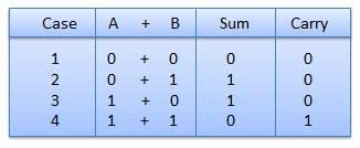
Binary Addition
|
In fourth step, a sum (1 + 1 = 10) i.e. 0 is written in the given column and a carry of 1 over to the next column is done.
For Example −
|
Fig: Binary addition
Binary Subtraction
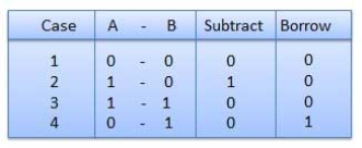
Subtraction and Borrow, these are the two words that will be used very frequently for binary subtraction. There rules of binary subtraction are:
|
For Example
|
Fig. Binary subtraction
Binary Multiplication
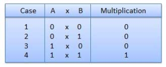
|
Fig. Rules of Binary Multiplication (Ref. 1)
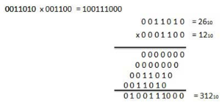
For Example
|
Fig. Binary Multiplication
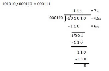
Binary Division
For Example
|
Fig. Binary Division
Logic Gates
The basic gates are namely AND gate, OR gate & NOT gate.
AND gate
It is a digital circuit that consists of two or more inputs and a single output which is the logical AND of all those inputs. It is represented with the symbol ‘.’.
The following is the truth table of 2-input AND gate.
A | B | Y = A.B |
0 | 0 | 0 |
0 | 1 | 0 |
1 | 0 | 0 |
1 | 1 | 1 |
Here A, B are the inputs and Y is the output of two input AND gate.
If both inputs are ‘1’, then only the output, Y is ‘1’. For remaining combinations of inputs, the output, Y is ‘0’.
The figure below shows the symbol of an AND gate, which is having two inputs A, B and one output, Y.
|
Fig. : AND gate (ref. 1)
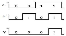
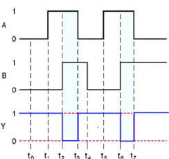
Timing Diagram:
|
OR gate
It is a digital circuit which has two or more inputs and a single output which is the logical OR of all those inputs. It is represented with the symbol ‘+’.
The truth table of 2-input OR gate is:
A | B | Y = A + B |
0 | 0 | 0 |
0 | 1 | 1 |
1 | 0 | 1 |
1 | 1 | 1 |
Here A, B are the inputs and Y is the output of two input OR gate.
When both inputs are ‘0’, then only the output, Y is ‘0’. For remaining combinations of inputs, the output, Y is ‘1’.
The figure below shows the symbol of an OR gate, which is having two inputs A, B and one output, Y.
|
Fig. : OR gate (ref. 1)
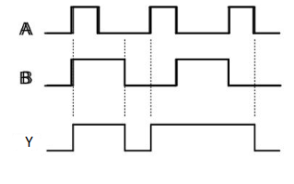
Timing Diagram:
|
NOT gate
It is a digital circuit that has one input and one output. Here the output is the logical inversion of input. Hence, it is also called as an inverter.
The truth table of NOT gate is:
A | Y = A’ |
0 | 1 |
1 | 0 |
Here A and Y are the corresponding input and output of NOT gate. When A is ‘0’, then, Y is ‘1’. Similarly, when, A is ‘1’, then, Y is ‘0’.
The figure below shows the symbol of NOT gate, which has one input, A and one output, Y.
|
Fig. : NOT gate (ref. 1)
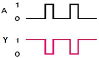
Timing Diagram:
|
Universal gates
The Universal gates are namely NAND gate and NOR gate
The NAND gate and NOR gate
NAND gate
It is a digital circuit which has two or more inputs and single output and it is the inversion of logical AND gate.
The truth table of 2-input NAND gate is:
A | B | Y = (A.B)’ |
0 | 0 | 1 |
0 | 1 | 1 |
1 | 0 | 1 |
1 | 1 | 0 |
Here A, B are the inputs and Y is the output of two input NAND gate. When both inputs are ‘1’, then the output, Y is ‘0’. If at least one of the inputs is zero, then the output, Y is ‘1’. This is just the inverse of AND operation.
The image shows the symbol of NAND gate:
|
Fig.: NAND gate (ref. 1)
NAND gate works same as AND gate followed by an inverter.
Timing Diagram:
|
NOR gate
It is a digital circuit that has two or more inputs and a single output which is the inversion of logical OR of all inputs.
The truth table of 2-input NOR gate is:
A | B | Y = (A+B)’ |
0 | 0 | 1 |
0 | 1 | 0 |
1 | 0 | 0 |
1 | 1 | 0 |
Here A and B are the two inputs and Y is the output. If both inputs are ‘0’, then the output is ‘1’. If any one of the inputs is ‘1’, then the output is ‘0’. This is exactly opposite to two input OR gate operation.
The symbol of NOR gate is:
|
Fig.: NOR gate (ref. 1)
NOR gate works exactly same as that of OR gate followed by an inverter.
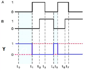
Timing Diagram:
|
4.3 Using Boolean algebra simplification of Boolean function
Postulates and Basic Laws of Boolean Algebra
Here, the Boolean postulates and basic laws that are used are given underneath.
Boolean Postulates
x + 0 = x
x + 1 = 1
x + x = x
x + x’ = 1
x.1 = x
x.0 = 0
x.x = x
x.x’ = 0
Basic Laws of Boolean Algebra
Commutative Law
x + y = y + x
x.y = y.x
Associative Law
x + (y + z) = (x + y) + z
x.(y.z) = (x.y).z
Distributive Law
x.(y + z) = x.y + x.z
x + (y.z) = (x + y).(x + z)
Theorems of Boolean Algebra
- Duality theorem
- De Morgan’s theorem
Duality Theorem
Group1 | Group2 |
x + 0 = x | x.1 = x |
x + 1 = 1 | x.0 = 0 |
x + x = x | x.x = x |
x + x’ = 1 | x.x’ = 0 |
x + y = y + x | x.y = y.x |
x + (y + z) = (x + y) + z | x.(y.z) = (x.y).z |
x.(y + z) = x.y + x.z | x + (y.z) = (x + y).(x + z) |
De Morgan’s Theorem
(x + y)’ = x’.y’
(x.y)’ = x’ + y’
Simplification of Boolean Functions
Numerical
f = p’qr + pq’r + pqr’ + pqr
Method 1
Given
f = p’qr + pq’r + pqr’ +pqr.
In first and second term r is common and in third and fourth terms pq is common.
So, taking out the common terms by using Distributive law we get,
⇒ f = (p’q + pq’)r + pq(r’ + r)
The terms present in first parenthesis can be simplified by using Ex-OR operation.
The terms present in second parenthesis is equal to ‘1’ using Boolean postulate we get
⇒ f = (p ⊕q)r + pq(1)
The first term can’t be simplified further.
But, the second term is equal to pq using Boolean postulate.
⇒ f = (p ⊕q)r + pq
Therefore, the simplified Boolean function is f = (p⊕q)r + pq
Method 2
Given f = p’qr + pq’r + pqr’ + pqr.
Using the Boolean postulate, x + x = x.
Hence we can write the last term pqr two more times.
⇒ f = p’qr + pq’r + pqr’ + pqr + pqr + pqr
Now using the Distributive law for 1st and 4th terms, 2nd and 5th terms, 3rdand 6th terms we get.
⇒ f = qr(p’ + p) + pr(q’ + q) + pq(r’ + r)
Using Boolean postulate, x + x’ = 1 and x.1 = x for further simplification .
⇒ f = qr(1) + pr(1) + pq(1)
⇒ f = qr + pr + pq
⇒ f = pq + qr + pr
Therefore, the simplified Boolean function is f = pq + qr + pr.
Hence we got two different Boolean functions after simplification of the given Boolean function. Functionally, these two functions are same. As per requirement, we can choose one of them.
Numerical
Find the complement of the Boolean function,
f = p’q + pq’.
Solution:
Using DeMorgan’s theorem, (x + y)’ = x’.y’ we get
⇒ f’ = (p’q)’.(pq’)’
Then by second law, (x.y)’ = x’ + y’ we get
⇒ f’ = {(p’)’ + q’}.{p’ + (q’)’}
Then by using, (x’)’=x we get
⇒ f’ = {p + q’}.{p’ + q}
⇒ f’ = pp’ + pq + p’q’ + qq’
Using x.x’=0 we get
⇒ f = 0 + pq + p’q’ + 0
⇒ f = pq + p’q’
Therefore, the complement of Boolean function, p’q + pq’ is pq + p’q’.
Canonical & Standard Forms
The following table represents the min terms and MAX terms for 2 variables.
x | y | Min terms | Max terms |
0 | 0 | m0=x’y’ | M0=x + y |
0 | 1 | m1=x’y | M1=x + y’ |
1 | 0 | m2=xy’ | M2=x’ + y |
1 | 1 | m3=xy | M3=x’ + y’ |
Canonical SoP and PoS forms
Therefore, we can express each output variable in two ways.
Canonical SoP form
Example
Considering the following truth table.
Inputs | Output | ||
P | q | r | f |
0 | 0 | 0 | 0 |
0 | 0 | 1 | 0 |
0 | 1 | 0 | 0 |
0 | 1 | 1 | 1 |
1 | 0 | 0 | 0 |
1 | 0 | 1 | 1 |
1 | 1 | 0 | 1 |
1 | 1 | 1 | 1 |
f = p’qr + pq’r + pqr’ + pqr.
f=m3+m5+m6+m7f=m3+m5+m6+m7
f=∑m(3,5,6,7)f=∑m(3,5,6,7)
Canonical PoS form
Standard SoP and PoS forms
Standard SoP form
Standard SoP of output variable can be obtained by two steps.
The same procedure is followed for other output variables too, if there is more than one output variable.
Numerical
Convert the Boolean function into Standard SoP form.
f = p’qr + pq’r + pqr’ + pqr
Solution:
Step 1 – By using the Boolean postulate, x + x = x and also writing the last term pqr two more times we get
⇒ f = p’qr + pq’r + pqr’ + pqr + pqr + pqr
Step 2 – By Using Distributive law for 1st and 4th terms, 2nd and 5th terms, 3rdand 6th terms.
⇒ f = qr(p’ + p) + pr(q’ + q) + pq(r’ + r)
Step 3 – Then Using Boolean postulate, x + x’ = 1 we get
⇒ f = qr(1) + pr(1) + pq(1)
Step 4 – hence using Boolean postulate, x.1 = x we get
⇒ f = qr + pr + pq
⇒ f = pq + qr + pr
This is the required Boolean function.
Standard PoS form
Standard PoS form of output variable is obtained by two steps.
The same procedure is followed for other output variables too.
Numerical
Convert the Boolean function into Standard PoS form.
f = (p + q + r).(p + q + r’).(p + q’ + r).(p’ + q + r)
Solution:
Step 1 – By using the Boolean postulate, x.x = x and writing the first term p+q+r two more times we get
⇒ f = (p + q + r).(p + q + r).(p + q + r).(p + q + r’).(p +q’ + r).(p’ + q + r)
Step 2 – Now by using Distributive law, x + (y.z) = (x + y).(x + z) for 1st and 4thparenthesis, 2nd and 5th parenthesis, 3rd and 6th parenthesis.
⇒ f = (p + q + rr’).(p + r + qq’).(q + r + pp’)
Step 3 − Applying Boolean postulate, x.x’=0 for simplifying of the terms present in each parenthesis.
⇒ f = (p + q + 0).(p + r + 0).(q + r + 0)
Step 4 − Using Boolean postulate, x + 0 = x we get
⇒ f = (p + q).(p + r).(q + r)
⇒ f = (p + q).(q + r).(p + r)
This is the simplified Boolean function.
Hence, both Standard SoP and Standard PoS forms are Dual to one another.
K-maps
There are 2 forms in converting a Boolean equation into K-map:
Un-optimized form
Optimized form
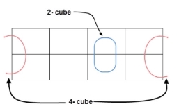
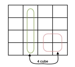
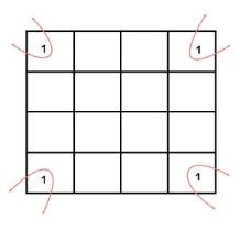
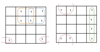
Grouping of K-map variables
|
|
2 variable K-maps
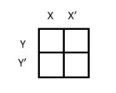
There are 4 cells (22) in the 2-variable k-map. It will look like (see below image)
|
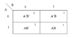
The possible min terms with 2 variables (A and B) are A.B, A.B’, A’.B and A’.B’. The conjunctions of the variables (A, B) and (A’, B) are represented in the cells of the top row and (A, B’) and (A’, B’) in cells of the bottom row. The following table shows the positions of all the possible outputs of 2-variable Boolean function on a K-map.
|
A general representation of a 2 variable K-map plot is shown below.
|
When we are simplifying a Boolean equation using Karnaugh map, we represent each cell of K-map containing the conjunction term with 1. After that, we group the adjacent cells with possible sizes as 2 or 4. In case of larger k-maps, we can group the variables in larger sizes like 8 or 16.
The groups of variables should be in rectangular shape that means the groups must be formed by combining adjacent cells either vertically or horizontally. Diagonal shaped or L-shaped groups are not allowed. The following example demonstrates a K-map simplification of a 2-variable Boolean equation.
ExampleSimplify the given 2-variable Boolean equation by using K-map.
F = X Y’ + X’ Y + X’Y’
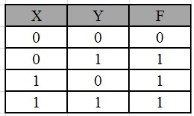
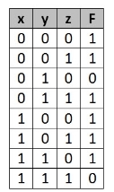
First, let’s construct the truth table for the given equation,
|
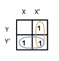
We put 1 at the output terms given in equation.
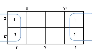
|
In this K-map, we can create 2 groups by following the rules for grouping, one is by combining (X’, Y) and (X’, Y’) terms and the other is by combining (X, Y’) and (X’, Y’) terms. Here the lower right cell is used in both groups.
After grouping the variables, the next step is determining the minimized expression.
By reducing each group, we obtain a conjunction of the minimized expression such as by taking out the common terms from two groups, i.e. X’ and Y’. So the reduced equation will be X’ +Y’.
3 variable K-maps
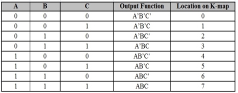
For a 3-variable Boolean function, there is a possibility of 8 output min terms. The general representation of all the min terms using 3-variables is shown below.
|
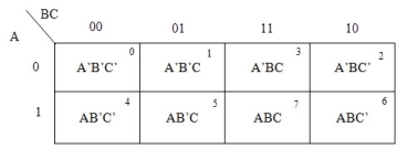
A typical plot of a 3-variable K-map is shown below. It can be observed that the positions of columns 10 and 11 are interchanged so that there is only change in one variable across adjacent cells. This modification will allow in minimizing the logic.
|
Up to 8 cells can be grouped in case of a 3-variable K-map with other possibilities being 1, 2 and 4.
Example
Simplify the given 3-variable Boolean equation by using k-map.
F = X’ Y Z + X’ Y’ Z + X Y Z’ + X’ Y’ Z’ + X Y Z + X Y’ Z’
First, let’s construct the truth table for the given equation,
|
We put 1 at the output terms given in equation.
There are 8 cells (23) in the 3-variable k-map. It will look like (see below image).
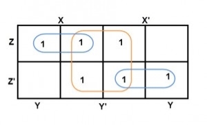
The largest group size will be 8 but we can also form the groups of size 4 and size 2, by possibility. In the 3 variable Karnaugh map, we consider the left most column of the k-map as the adjacent column of rightmost column. So the size 4 group is formed as shown below.
|
And in both the terms, we have ‘Y’ in common. So the group of size 4 is reduced as the conjunction Y. To consume every cell which has 1 in it, we group the rest of cells to form size 2 group, as shown below.
|
The 2 size group has no common variables, so they are written with their variables and its conjugates. So the reduced equation will be X Z’ + Y’ + X’ Z. In this equation, no further minimization is possible.
4 variable K-maps
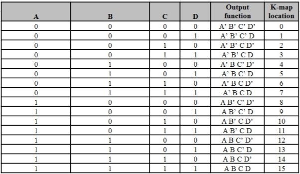
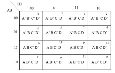
There are 16 possible min terms in case of a 4-variable Boolean function. The general representation of min terms using 4 variables is shown below.
|
A typical 4-variable K-map plot is shown below. It can be observed that both the columns and rows of 10 and 11 are interchanged.
|
The possible numbers of cells that can be grouped together are 1, 2, 4, 8 and 16.
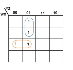
ExampleSimplify the given 4-variable Boolean equation by using k-map. F (W, X, Y, Z) = (1, 5, 12, 13)
Sol: F (W, X, Y, Z) = (1, 5, 12, 13)
|
By preparing k-map, we can minimize the given Boolean equation as
F = W Y’ Z + W ‘Y’ Z
5 variable K-maps
A 5-variable Boolean function can have a maximum of 32 min terms. All the possible min terms are represented below
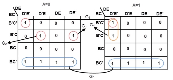
In 5-variable K-map, we have 32 cells as shown below. It is represented by F (A, B, C, D, and E). It is divided into two grids of 16 cells with one variable (A) being 0 in one grid and 1 in other grid.
|
Example
Simplify the given 5-variable Boolean equation by using k-map.
f (A, B, C, D, E) = ∑ m (0, 5, 6, 8, 9, 10, 11, 16, 20, 42, 25, 26, 27)
|
4.5 Introduction to IC Technology
The concept of IC was first introduced in the year 1958. Since then this concept has reached great technological heights than any other concepts and has helped in the miniaturization of a lot of components like mobiles, computers, laptops, and many more devices in the digital world.
The digital era started with the invention of vacuum tubes. Vacuum based computers were rare and expensive. This was then replaced by transistors, which were faster in use and smaller in size, cost effective, less power consuming and reliable. Then came the invention of integrated circuits which just revolutionized the use of computers. Due to its small dimension, low cost, and very high reliability even the common man is familiar with its applications like smart phones and laptops.
The IC’s also found its way in military applications, state of the art communication systems, and industrial applications due to its high reliability and compact size. Nowadays, an IC that has the size of a fingernail consists of more than a million transistors and other discrete components embedded into it. Thus an integrated circuit can also be called a microchip and is basically a collection of some discrete circuits on a small chip that is made of a semiconductor material like silicon.
The use of discrete circuits was replaced by IC’s due to two factors. One is space consumption. A discrete circuitry consists of transistors, resistors, diodes, capacitors, and many other discrete devices. Each of them is soldered on to printed circuit boards (PCB) according to the need of circuitry. In the end PCB will occupy a large space. Another drawback is that the soldered components will show less reliability due to the use of many components. Both these factors urged engineers to invent microcircuits that have more reliability and consume less space.
ICs can be classified on the basis of their chip size as given below:
Small scale integration (SSI)—3 to 30 gates/chip.
Medium scale integration (MSI)—30 to 300 gates/chip.
Large scale integration (LSI)—300 to 3,000 gates/chip.
Very large-scale integration (VLSI)—more than 3,000 gates/chip.
References:
