Unit – 1
Introduction
Functional Units of Digital System.
1 A computer organization describes the functions and design of the various units of a digital system.
2 A general-purpose computer system is the best-known example of a digital system. Other examples include telephone switching exchanges, digital voltmeters, digital counters, electronic calculators and digital displays.
3 Computer architecture deals with the specification of the instruction set and the hardware units that implement the instructions.
4 Computer hardware consists of electronic circuits, displays, magnetic and optic storage media and also the communication facilities.
5 Functional units are a part of a CPU that performs the operations and calculations called for by the computer program.
6 Functional units of a computer system are parts of the CPU (Central Processing Unit) that performs the operations and calculations called for by the computer program. A computer consists of five main components namely, Input unit, Central Processing Unit, Memory unit Arithmetic & logical unit, Control unit and an Output unit
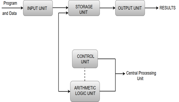
Input unit
1 Input units are used by the computer to read the data. The most commonly used input devices are keyboards, mouse, joysticks, trackballs, microphones, etc.
2 However, the most well-known input device is a keyboard. Whenever a key is pressed, the corresponding letter or digit is automatically translated into its corresponding binary code and transmitted over a cable to either the memory or the processor.
Central processing unit
Central processing unit commonly known as CPU can be referred as an electronic circuitry within a computer that carries out the instructions given by a computer program by performing the basic arithmetic, logical, control and input/output (I/O) operations specified by the instructions.
Memory unit
1 The Memory unit can be referred to as the storage area in which programs are kept which are running, and that contains data needed by the running programs.
2 The Memory unit can be categorized in two ways namely, primary memory and secondary memory.
3 It enables a processor to access running execution applications and services that are temporarily stored in a specific memory location.
4 Primary storage is the fastest memory that operates at electronic speeds. Primary memory contains a large number of semiconductor storage cells, capable of storing a bit of information. The word length of a computer is between 16-64 bits.
5 It is also known as the volatile form of memory, means when the computer is shut down, anything contained in RAM is lost.
6 Cache memory is also a kind of memory which is used to fetch the data very soon. They are highly coupled with the processor.
7 The most common examples of primary memory are RAM and ROM.
8 Secondary memory is used when a large amount of data and programs have to be stored for a long-term basis.
9 It is also known as the Non-volatile memory form of memory, means the data is stored permanently irrespective of shut down.
10 The most common examples of secondary memory are magnetic disks, magnetic tapes, and optical disks.
Arithmetic & logical unit
Most of all the arithmetic and logical operations of a computer are executed in the ALU (Arithmetic and Logical Unit) of the processor. It performs arithmetic operations like addition, subtraction, multiplication, division and also the logical operations like AND, OR, NOT operations.
Control unit
1 The control unit is a component of a computer's central processing unit that coordinates the operation of the processor. It tells the computer's memory, arithmetic/logic unit and input and output devices how to respond to a program's instructions.
2 The control unit is also known as the nerve center of a computer system.
3 Let's us consider an example of addition of two operands by the instruction given as Add LOCA, RO. This instruction adds the memory location LOCA to the operand in the register RO and places the sum in the register RO. This instruction internally performs several steps.
Output Unit
1 The primary function of the output unit is to send the processed results to the user. Output devices display information in a way that the user can understand.
2 Output devices are pieces of equipment that are used to generate information or any other response processed by the computer. These devices display information that has been held or generated within a computer.
3 The most common example of an output device is a monitor.
A bus is a communication system in computer architecture that transfers data between components inside a computer, or between computers.
The term encompasses all the components related to hardware (wire, optical fibre, etc.) and software, including communication protocol.
The following are a few points to describe a computer bus:
- A bus is a group of lines/wires which carry computer signals.
- A bus is the means of shared transmission.
- Lines are assigned for providing descriptive names. — carries a single electrical signal, e.g. 1-bit memory address, data bits series, or timing control that turns the device on or off.
- Data can be transferred from one computer system location to another (between different I / O modules, memory, and CPU).
- The bus is not only cable but also hardware (bus architecture), protocol, program, and bus controller.
What are the different components of a bus?
Each bus possesses three distinct communication channels.
Following are the three components of a bus: –
- The address bus, a one-way pathway that allows information to pass in one direction only, carries information about where data is stored in memory.
- The data bus is a two-way pathway carrying the actual data (information) to and from the main memory.
- The control bus holds the control and timing signals needed to coordinate all of the computer’s activities.
Functions of a computer bus
Below are a few of the functions in a computer bus:
- Data sharing – All types of buses used in network transfer data between the connected computer peripherals. The buses either transfer or send data in serial or parallel transfer method. This allows 1, 2, 4, or even 8 bytes of data to be exchanged at a time. (A Byte is an 8-bit group). Buses are classified according to how many bits they can move simultaneously, meaning we have 8-bit, 16-bit, 32-bit, or even 64-bit buses.
- Addressing – A bus has address lines that suit the processors. This allows us to transfer data to or from different locations in the memory.
- Power – A bus supplies the power to various connected peripherals.
Structure and Topologies of Computer buses
Lines are grouped as mentioned below –
- Power line provides electrical power to the components connected
- Data lines carrying data or instructions between modules of the system
- Address lines indicate the recipient of the bus data
- Control lines control the synchronization and operation of the bus and the modules linked to the bus
What are the different types of computer buses?
Computers normally have two bus types:
- System bus – This is the bus that connects the CPU to the motherboard’s main memory. The system bus is also known as a front-side bus, a memory bus, a local bus, or a host bus.
- A number of I / O Buses, (I / O is an input/output acronym) connecting various peripheral devices to the CPU. These devices connect to the system bus through a ‘bridge’ implemented on the chipset of the processors. Other I / O bus names include “expansion bus,” “external bus” or “host bus”
Below are some of the types of Expansion buses:
ISA – Industry Standard Architecture
The Industry Standard Architecture (ISA) bus is still one of the oldest buses in service today.
Although it has been replaced by faster buses, ISA still has a lot of legacy devices that connect to it such as cash registers, CNC machines, and barcode scanners. Since being expanded to 16 bits in 1984, ISA remains largely unchanged. Additional high-speed buses were added to avoid performance problems.
EISA – Extended Industry Standard Architecture
An upgrade to ISA is Extended Industry Standard Architecture or EISA. This doubled the data channels from 16 to 32 and allowed the bus to be used by more than one CPU. Although deeper than the ISA slot, it is the same width that lets older devices connect to it.
When you compare the pins on an ISA to an EISA card (the gold portion of the card that goes into the slot), you can find that the EISA pins are longer and thinner. That is a quick way to decide if you have an ISA or an EISA card.
MCA – Micro Channel Architecture
IBM developed this bus as a substitute for ISA when they designed the PS/2 PC which was launched in 1987. The bus provided some technological improvements over the ISA bus. The MCA, for example, ran at a speed of 10MHz faster and supported either 16-bit or 32-bit data.
One advantage of MCA was that the plug-in cards were configurable software; that means they needed minimal user input during configuration.
VESA – Video Electronics Standards Association
The Video Electronics Standards Association (VESA) Local bus was created to divide the load and allow the ISA bus to handle interrupts, and the I / O port (input/output) and the VL bus to work with Direct Memory Access (DMA) and I / O memory. This was only a temporary solution, due to its size and other considerations. The PCI bus was easy to overtake the VL bus.
A VESA card has a range of additional pins and is longer than the ISA or EISA cards. It was created in the early ’90s and has a 32-bit bus and was a temporary fix designed to help boost ISA ‘s performance.
PCI – Peripheral Component Interconnect
The PCI bus was developed to solve ISA and VL-bus related issues. PCI has a 32-bit data path and will run at half the speed of the system memory bus.
One of its enhancements was to provide connected computers with direct access to machine memory. That increased computer efficiency while reducing the CPU ‘s capacity for interference.
Today’s computers mostly have PCI slots. PCI is considered a hybrid between ISA and VL-Bus that provides direct access to the connected devices system memory.
This uses a bridge to connect to the front side bus and CPU and is able to provide higher performance while reducing the potential for CPU interference.
PCI Express (PCI-X)
The most recent added slot is PCI Express (PCIe). It was designed to replace the AGP and PCI bus. It has a 64-bit data path and 133 MHz base speed but incorporating full-duplex architecture was the main performance enhancement.
That allowed the card to run in both directions at full speed simultaneously. PCI Express slots run at 1X, 4X, 8X, and 16X providing PCI with the highest transfer speed of any form of a slot. The multiplier specifies the maximum rate of transfer.
PCI Express is compatible backward, allowing a 1X card to fit into a 16X slot.
PCMCIA – Personal Computer Memory Card Industry Association (Also called PC bus)
The Personal Computer Memory Card Industry Association was established to give the laptop computers a standard bus. But it is used in small computers, essentially.
AGP – Accelerated Graphics Port
The Accelerated Graphics Bus (AGP) was designed to accommodate the computers’ increased graphics needs. It has a data path that is 32 bits long and runs at maximum bus speed.
This doubled the PCI bandwidth and reduced the need to share the bus with other components. This means that AGP operates at 66 MHz on a regular motherboard, instead of the 33 MHz of the PCI bus.
AGP has a base speed of 66 MHz that doubles PCI speed. You can also get slots that run at speeds 2X, 4X, and 8X.
It also uses special signalling to allow twice as much data to be transmitted at the same clock speed over the port.
SCSI – Small Computer Systems Interface.
Small Computer System Interface is a standard parallel interface used for attaching peripheral devices to a computer by Apple Macintosh computers, PCs, and Unix systems.
Most common types of computer buses
Most of the listed buses are no longer used or not frequently used today.
Below is a list of the buses that are the most popular ones:
- ESATA and SATA– Hard Drives and Disk Drives computer.
- PCIe – Video Cards and Computer Expansion Cards.
- USB – Peripherals to a computer.
- Thunderbolt – Peripherals that are connected via a USB-C cable.
Key takeaways
- A bus is a communication system in computer architecture that transfers data between components inside a computer, or between computers.
- The term encompasses all the components related to hardware (wire, optical fibre, etc.) and software, including communication protocol.
Bus is a group of wires that connects different components of the computer. It is used for transmitting data, control signal and memory address from one component to another. A bus can be 8 bit, 16 bit, 32 bit and 64 bit. A 32 bit bus can transmit 32 bit information at a time.
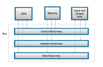
Fig -Bus Architecture
Data Bus:
Data Lines provide a path for moving data between system modules. It is bidirectional which means data lines are used to transfer data in both directions. For example, CPU can read data on these lines as well as send data out of these lines to a memory location or to a port.
Address bus:
Address Lines are collectively called as address bus. In any bus, the no. Of lines in address are usually 16, 20, 24, or more depending on type and architecture of bus. On these lines, CPU sends out the address of memory location on I/O Port that is to be written on or read from.
In short, it is an internal channel from CPU to Memory across which the address of data are transmitted. Here the communication is one way that is, the address is send from CPU to Memory and I/O Port but not Memory and I/O port send address to CPU on that line and hence these lines are unidirectional.
Control Bus:
Control Lines are collectively called as Control Bus. Control Lines are gateway used to transmit and receives control signals between the microprocessor and various devices attached to it. In other words, Control Lines are used by CPUs for Communicating with other devices within the computer.
Control Lines signals are:
Memory Read.
Memory Write.
I/O Read.
I/O Write.
Bus Request.
Bus Grant, etc.
There are mainly three types of Buses Data, Control and Address Bus as explained in above topic.
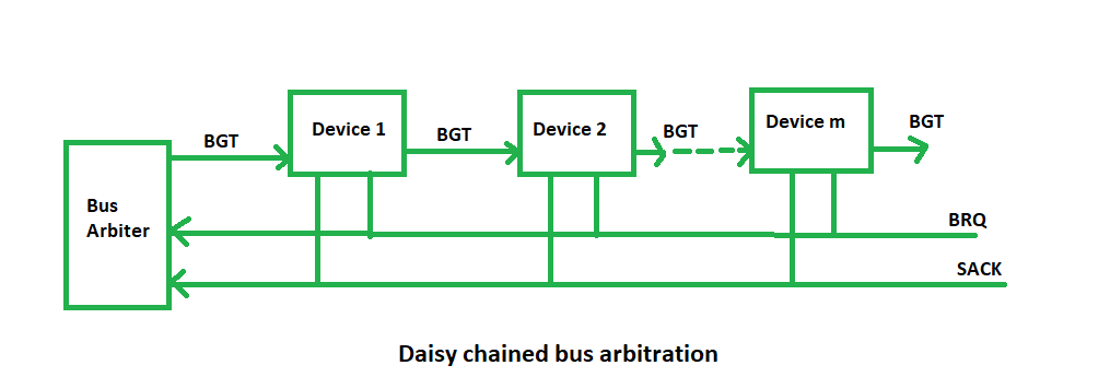
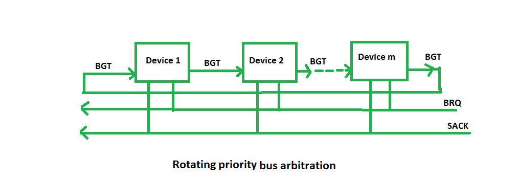
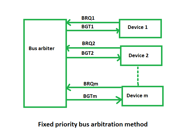
Bus Arbitration refers to the process by which the current bus master accesses and then leaves the control of the bus and passes it to the another bus requesting processor unit. The controller that has access to a bus at an instance is known as Bus master.
There are two approaches to bus arbitration:
- Centralized bus arbitration – A single bus arbiter performs the required arbitration.
- Distributed bus arbitration – All devices participate in the selection of the next bus master.
Methods of BUS Arbitration–
There are three bus arbitration methods:
(i)Daisy Chaining method–
It is a centralized bus arbitration method. During any bus cycle, the bus master may be any device – the processor or any DMA controller unit, connected to the bus.
(ii) Polling or Rotating Priority method –
In this method, the devices are assigned unique priorities and complete to access the bus, but the priorities are dynamically changed to give every device an opportunity to access the bus.
(iii) Fixed priority or Independent Request method –
In this method, the bus control passes from one device to another only through the centralized bus arbiter.
Memory Transfer
Most of the standard notations used for specifying operations on memory transfer are stated below.
- The transfer of information from a memory unit to the user end is called a Read operation.
- The transfer of new information to be stored in the memory is called a Write operation.
- A memory word is designated by the letter M.
- We must specify the address of memory word while writing the memory transfer operations.
- The address register is designated by AR and the data register by DR.
Thus, a read operation can be stated as
Read: DR ← M [AR]
The Read statement causes a transfer of information into the data register (DR) from the memory word (M) selected by the address register (AR).
And the corresponding write operation can be stated as:
Write: M [AR] ← R1
The Write statement causes a transfer of information from register R1 into the memory word (M) selected by address register (AR).
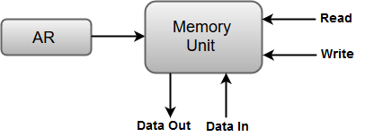
Fig- Showing Read and Write Operation.
Bus and Memory Transfers:
A bus consists of a set of common lines, one for each bit of register, through which binary information is transferred one at a time. Control signals determine which register is selected by the bus during a particular register transfer.
The following block diagram shows a Bus system for four registers. It is constructed with the help of four 4 * 1 Multiplexers each having four data inputs (0 through 3) and two selection inputs (S1 and S2).
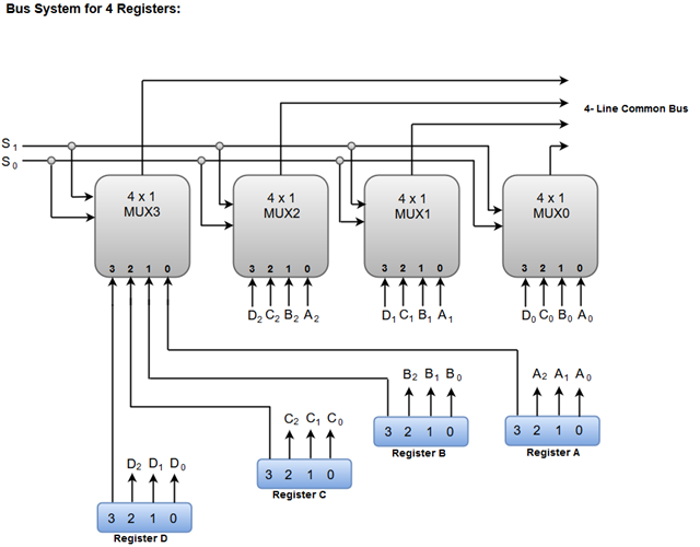
The two selection lines S1 and S2 are connected to the selection inputs of all four multiplexers. The selection lines choose the four bits of one register and transfer them into the four-line common bus.
When both of the select lines are at low logic, i.e. S1S0 = 00, the 0 data inputs of all four multiplexers are selected and applied to the outputs that forms the bus. This, in turn, causes the bus lines to receive the content of register A since the outputs of this register are connected to the 0 data inputs of the multiplexers.
Similarly, when S1S0 = 01, register B is selected, and the bus lines will receive the content provided by register B.
The following function table shows the register that is selected by the bus for each of the four possible binary values of the Selection lines.
S1 | S2 | Register Selected |
0 | 0 | A |
0 | 1 | B |
1 | 0 | C |
1 | 1 | D |
To understand the organization of the processor, let us consider the requirements placed on the processor, the things that it must do:
• Fetch instruction: The processor reads an instruction from memory (register, cache, main memory).
• Interpret instruction: The instruction is decoded to determine what action is required.
• Fetch data: The execution of an instruction may require reading data from memory or an I/O module.
• Process data: The execution of an instruction may require performing some arithmetic or logical operation on data.
• Write data: The results of an execution may require writing data to memory or an I/O module.
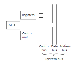
Fig- CPU with System Bus.
More Detailed Structure of CPU is shown below
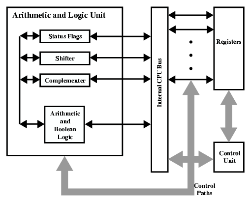
Fig- Internal Structure of CPU.
REGISTER ORGANISATION A computer system employs a memory hierarchy. At higher levels of the hierarchy, memory is faster, smaller, and more expensive (per bit). Within the processor, there is a set of registers that function as a level of memory above main memory and cache in the hierarchy.
The registers in the processor perform two roles:
• User-visible registers: Enable the machine- or assembly language programmer to minimize main memory references by optimizing use of registers.
• Control and status registers: Used by the control unit to control the operation of the processor and by privileged, operating system programs to control the execution of programs. User-Visible Registers A user-visible register is one that may be referenced by means of the machine language that the processor executes.
We can characterize these in the following categories:
• General purpose
• Data
• Address
• Condition codes
General-purpose registers can be assigned to a variety of functions by the programmer. Sometimes their use within the instruction set is orthogonal to the operation. That is, any general-purpose register can contain the operand for any opcode. This provides true general-purpose register use. There may be dedicated registers for floating-point and stack operations.
In some cases, general-purpose registers can be used for addressing functions (e.g., register indirect, displacement).
Data registers may be used only to hold data and cannot be employed in the calculation of an operand address.
Address registers may themselves be somewhat general purpose, or they may be devoted to a particular addressing mode.
Examples include the following:
• Segment pointers: In a machine with segmented addressing, a segment register holds the address of the base of the segment.
• Index registers: These are used for indexed addressing and may be auto indexed.
• Stack pointer: If there is user-visible stack addressing, then typically there is a dedicated register that points to the top of the stack. There are several design issues to be addressed here.
An important issue is whether to use completely general-purpose registers or to specialize their use.
Another design issue is the number of registers, general purpose or data plus address, to be provided.
Again, this affects instruction set design because more registers require more operand specifier bits.
Finally, there is the issue of register length. Registers that must hold addresses obviously must be at least long enough to hold the largest address.
Data registers should be able to hold values of most data types. Some machines allow two contiguous registers to be used as one for holding double-length values.
Stack Organization
Stack is a storage structure that stores information in such a way that the last item stored is the first item retrieved. It is based on the principle of LIFO (Last-in-first-out). The stack in digital computers is a group of memory locations with a register that holds the address of top of element. This register that holds the address of top of element of the stack is called Stack Pointer.
Stack Operations:
The two operations of a stack are:
- Push: Inserts an item on top of stack.
- Pop: Deletes an item from top of stack.
Implementation of Stack:
In digital computers, stack can be implemented in two ways:
- Register Stack
- Memory Stack
Register Stack
A stack can be organized as a collection of finite number of registers that are used to store temporary information during the execution of a program. The stack pointer (SP) is a register that holds the address of top of element of the stack.
Memory Stack
A stack can be implemented in a random access memory (RAM) attached to a CPU. The implementation of a stack in the CPU is done by assigning a portion of memory to a stack operation and using a processor register as a stack pointer. The starting memory location of the stack is specified by the processor register as stack pointer.
Addressing modes
Addressing Modes– The term addressing modes refers to the way in which the operand of an instruction is specified. The addressing mode specifies a rule for interpreting or modifying the address field of the instruction before the operand is actually executed.
Addressing modes for 8086 instructions are divided into two categories:
1) Addressing modes for data
2) Addressing modes for branch
The 8086 memory addressing modes provide flexible access to memory, allowing you to easily access variables, arrays, records, pointers, and other complex data types. The key to good assembly language programming is the proper use of memory addressing modes.
An assembly language program instruction consists of two parts

Fig - Assembly language program instruction
The memory address of an operand consists of two components:
IMPORTANT TERMS
- Starting address of memory segment.
- Effective address or Offset: An offset is determined by adding any combination of three address elements: displacement, base and index.
- Displacement: It is an 8 bit or 16 bit immediate value given in the instruction.
- Base: Contents of base register, BX or BP.
- Index: Content of index register SI or DI.
According to different ways of specifying an operand by 8086 microprocessor, different addressing modes are used by 8086.
Addressing modes used by 8086 microprocessors are discussed below:
- Implied mode: In implied addressing the operand is specified in the instruction itself. In this mode the data is 8 bits or 16 bits long and data is the part of instruction. Zero address instruction are designed with implied addressing mode.

Example: CLC (used to reset Carry flag to 0)
- Immediate addressing mode (symbol #):In this mode data is present in address field of instruction .Designed like one address instruction format.
Note: Limitation in the immediate mode is that the range of constants are restricted by size of address field.
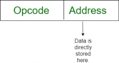
Example: MOV AL, 35H (move the data 35H into AL register)
- Register mode: In register addressing the operand is placed in one of 8 bit or 16-bit general purpose registers. The data is in the register that is specified by the instruction.
Here one register reference is required to access the data.

Example: MOV AX, CX (move the contents of CX register to AX register)
- Register Indirect mode: In this addressing the operand’s offset is placed in any one of the registers BX,BP,SI,DI as specified in the instruction. The effective address of the data is in the base register or an index register that is specified by the instruction.
Here two register reference is required to access the data.

Fig – Register Indirect mode
The 8086 CPUs let you access memory indirectly through a register using the register indirect addressing modes.
- MOV AX, [BX](move the contents of memory location
Addressed by the register BX to the register AX)
- Auto Indexed (increment mode): Effective address of the operand is the contents of a register specified in the instruction. After accessing the operand, the contents of this register are automatically incremented to point to the next consecutive memory location.(R1)+.
Here one register reference, one memory reference and one ALU operation is required to access the data.
Example:
- Add R1, (R2)+ // OR
- R1 = R1 +M[R2]
R2 = R2 + d
Useful for stepping through arrays in a loop. R2 – start of array d – size of an element
- Auto indexed (decrement mode): Effective address of the operand is the contents of a register specified in the instruction. Before accessing the operand, the contents of this register are automatically decremented to point to the previous consecutive memory location. –(R1)
Here one register reference, one memory reference and one ALU operation is required to access the data.
Example:
Add R1, -(R2) //OR
R2 = R2-d
R1 = R1 + M[R2]
Auto decrement mode is same as auto increment mode. Both can also be used to implement a stack as push and pop. Auto increment and Auto decrement modes are useful for implementing “Last-In-First-Out” data structures.
- Direct addressing/ Absolute addressing Mode (symbol [ ]): The operand’s offset is given in the instruction as an 8 bit or 16 bit displacement element. In this addressing mode the 16-bit effective address of the data is the part of the instruction.
Here only one memory reference operation is required to access the data.

Example: ADD AL, [0301] //add the contents of offset address 0301 to AL
- Indirect addressing Mode (symbol @ or ()): In this mode address field of instruction contains the address of effective address. Here two references are required.
1st reference to get effective address.
2nd reference to access the data.
Based on the availability of Effective address, Indirect mode is of two kind:
- Register Indirect: In this mode effective address is in the register, and corresponding register name will be maintained in the address field of an instruction.
Here one register reference, one memory reference is required to access the data. - Memory Indirect: In this mode effective address is in the memory, and corresponding memory address will be maintained in the address field of an instruction.
Here two memory reference is required to access the data.
- Indexed addressing mode: The operand’s offset is the sum of the content of an index register SI or DI and an 8 bit or 16-bit displacement.
Example AX, [SI +05]
- Based Indexed Addressing: The operand’s offset is sum of the content of a base register BX or BP and an index register SI or DI.
Example: ADD AX, [BX+SI]
Based on Transfer of control, addressing modes are:
- PC relative addressing mode: PC relative addressing mode is used to implement intra segment transfer of control, In this mode effective address is obtained by adding displacement to PC.
- EA= PC + Address field value
PC= PC + Relative value.
3. Base register addressing mode: Base register addressing mode is used to implement inter segment transfer of control. In this mode effective address is obtained by adding base register value to address field value.
4. EA= Base register + Address field value.
5. PC= Base register + Relative value.
Note:
PC relative nad based register both addressing modes are suitable for program relocation at runtime.
Based register addressing mode is best suitable to write position independent codes.
Advantages of Addressing Modes
To give programmers to facilities such as Pointers, counters for loop controls, indexing of data and program relocation.
To reduce the number bits in the addressing field of the Instruction.
Key takeaway
Addressing Modes– The term addressing modes refers to the way in which the operand of an instruction is specified. The addressing mode specifies a rule for interpreting or modifying the address field of the instruction before the operand is actually executed.
References:
1. Computer System Architecture - M. Mano
2. Carl Hamacher, Zvonko Vranesic, Safwat Zaky Computer Organization, McGraw-Hill, Fifth Edition, Reprint 2012
3. John P. Hayes, Computer Architecture and Organization, Tata McGraw Hill, Third Edition, 1998. Reference books
4. William Stallings, Computer Organization and Architecture-Designing for Performance, Pearson Education, Seventhedition, 2006.
5. Behrooz Parahami, “Computer Architecture”, Oxford University Press, Eighth Impression, 2011.