Unit – 4
Memory
A memory unit is the collection of storage units or devices together. The memory unit stores the binary information in the form of bits.
Memory Hierarchy is an enhancement to organize the memory such that it can minimize the access time. The Memory Hierarchy was developed based on a program behaviour known as locality of references.
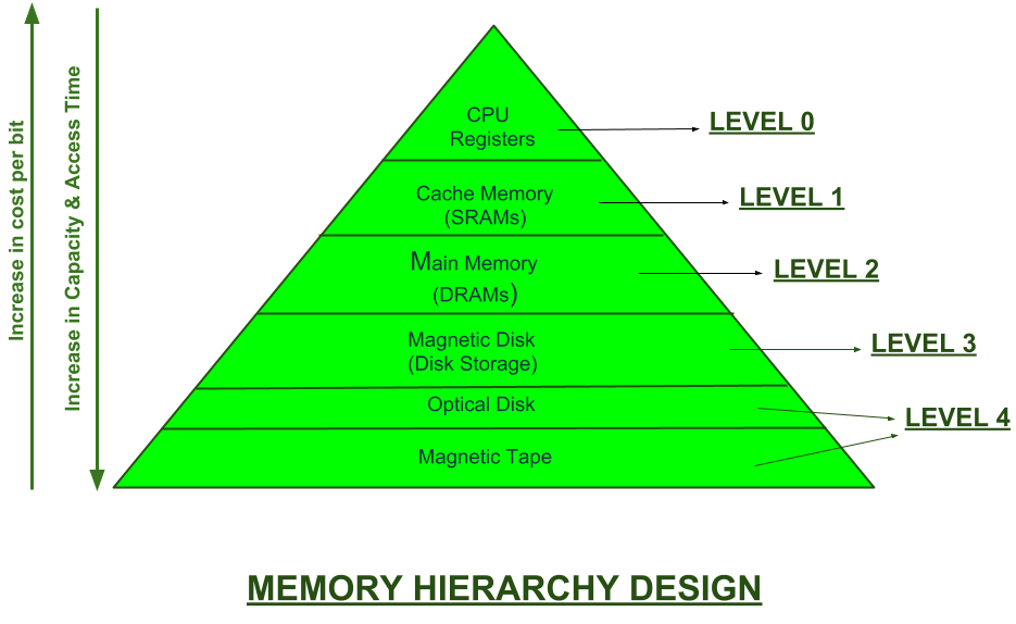
Memory Hierarchy is divided into 2 main types:
- External Memory or Secondary Memory –
Comprising of Magnetic Disk, Optical Disk, Magnetic Tape i.e. peripheral storage devices which are accessible by the processor via I/O Module.
2. Internal Memory or Primary Memory –
Comprising of Main Memory, Cache Memory & CPU registers. This is directly accessible by the processor.
Memory Access Methods:
Each Memory is a collection of numerous memory locations. To access data from any memory, first it must be located and then the data is read from the memory location.
Access Methods in Memory:
- Random Access: Main memories are random access memories, in which each memory location has a unique address. Using this unique address any memory location can be reached in the same amount of time in any order.
- Sequential Access: This method allows memory access in a sequence or in order.
- Direct Access: In this mode, information is stored in tracks, with each track having a separate read/write head.
Levels of memory:
- Level 1 or Register.
It is a type of memory in which data is stored and accepted that are immediately stored in CPU. Most commonly used register is accumulator, Program counter, address register etc.
- Level 2 or Cache memory.
It is the fastest memory which has faster access time where data is temporarily stored for faster access.
- Level 3 or Main Memory.
It is memory on which computer works currently. It is small in size and once power is off data no longer stays in this memory.
- Level 4 or Secondary Memory.
It is external memory which is not as fast as main memory but data stays permanently in this memory.
Semiconductor memory is used in any electronics assembly that uses computer processing technology. Semiconductor memory is the essential electronics component needed for any computer-based PCB assembly.
In addition to this, memory cards have become commonplace items for temporarily storing data - everything from the portable flash memory cards used for transferring files, to semiconductor memory cards used in cameras, mobile phones and the like.
The use of semiconductor memory has grown, and the size of these memory cards has increased as the need for larger and larger amounts of storage is needed.
To meet the growing needs for semiconductor memory, there are many types and technologies that are used. As the demand grows new memory technologies are being introduced and the existing types and technologies are being further developed.
A variety of different memory technologies are available - each one suited to different applications. Names such as ROM, RAM, EPROM, EEPROM, Flash memory, DRAM, SRAM, SDRAM, as well as F-RAM and MRAM are available, and new types are being developed to enable improved performance.
Terms like DDR3, DDR4, DDR5 and many more are seen and these refer to different types of SDRAM semiconductor memory.
In addition to this the semiconductor devices are available in many forms - ICs for printed board assembly, USB memory cards, Compact Flash cards, SD memory cards and even solid-state hard drives. Semiconductor memory is even incorporated into many microprocessor chips as on-board memory.
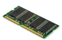
Fig - Printed circuit board containing computer memory
Semiconductor memory: main types
There are two main types or categories that can be used for semiconductor technology. These memory types or categories differentiate the memory to the way in which it operates:
RAM - Random Access Memory: As the names suggest, the RAM or random-access memory is a form of semiconductor memory technology that is used for reading and writing data in any order - in other words as it is required by the processor. It is used for such applications as the computer or processor memory where variables and other stored and are required on a random basis. Data is stored and read many times to and from this type of memory.
Random access memory is used in huge quantities in computer applications as current day computing and processing technology requires large amounts of memory to enable them to handle the memory hungry applications used today. Many types of RAM including SDRAM with its DDR3, DDR4, and soon DDR5 variants are used in huge quantities.
ROM - Read Only Memory: A ROM is a form of semiconductor memory technology used where the data is written once and then not changed. In view of this it is used where data needs to be stored permanently, even when the power is removed - many memory technologies lose the data once the power is removed.
As a result, this type of semiconductor memory technology is widely used for storing programs and data that must survive when a computer or processor is powered down. For example, the BIOS of a computer will be stored in ROM. As the name implies, data cannot be easily written to ROM. Depending on the technology used in the ROM, writing the data into the ROM initially may require special hardware. Although it is often possible to change the data, this gain requires special hardware to erase the data ready for new data to be written in.
As can be seen, these two types of memory are very different, and as a result they are used in very different ways.
Each of the semiconductor memory technologies outlined below falls into one of these two types of category. Each technology offers its own advantages and is used in a particular way, or for a particular application.
Semiconductor memory technologies
There is a large variety of types of ROM and RAM that are available. Often the overall name for the memory technology includes the initials RAM or ROM and this gives a guide as to the overall type of format for the memory.
With technology moving forwards apace, not only are the established technologies moving forwards with SDRAM technology moving from DDR3 to DDR4 and then to DDR5, but Flash memory used in memory cards is also developing as are the other technologies.
In addition to this, new memory technologies are arriving on the scene and they are starting to make an impact in the market, enabling processor circuits to perform more effectively.
The different memory types or memory technologies are detailed below:
DRAM: Dynamic RAM is a form of random-access memory. DRAM uses a capacitor to store each bit of data, and the level of charge on each capacitor determines whether that bit is a logical 1 or 0. However these capacitors do not hold their charge indefinitely, and therefore the data needs to be refreshed periodically. As a result of this dynamic refreshing, it gains its name of being a dynamic RAM. DRAM is the form of semiconductor memory that is often used in equipment including personal computers and workstations where it forms the main RAM for the computer. The semiconductor devices are normally available as integrated circuits for use in PCB assembly in the form of surface mount devices or less frequently now as leaded components.
EEPROM: This is an Electrically Erasable Programmable Read Only Memory. Data can be written to these semiconductor devices and it can be erased using an electrical voltage. This is typically applied to an erase pin on the chip. Like other types of PROM, EEPROM retains the contents of the memory even when the power is turned off. Also, like other types of ROM, EEPROM is not as fast as RAM.
EPROM: This is an Erasable Programmable Read Only Memory. These semiconductor devices can be programmed and then erased at a later time. This is normally achieved by exposing the semiconductor device itself to ultraviolet light. To enable this to happen there is a circular window in the package of the EPROM to enable the light to reach the silicon of the device. When the PROM is in use, this window is normally covered by a label, especially when the data may need to be preserved for an extended period. The PROM stores its data as a charge on a capacitor. There is a charge storage capacitor for each cell and this can be read repeatedly as required. However, it is found that after many years the charge may leak away and the data may be lost. Nevertheless, this type of semiconductor memory used to be widely used in applications where a form of ROM was required, but where the data needed to be changed periodically, as in a development environment, or where quantities were low.
Flash memory: Flash memory may be considered as a development of EEPROM technology. Data can be written to it and it can be erased, although only in blocks, but data can be read on an individual cell basis.
To erase and re-programme areas of the chip, programming voltages at levels that are available within electronic equipment are used. It is also non-volatile, and this makes it particularly useful. As a result, Flash memory is widely used in many applications including USB memory sticks, compact Flash memory cards, SD memory cards and also now solid-state hard drives for computers and many other applications.
F-RAM: Ferroelectric RAM is a random-access memory technology that has many similarities to the standard DRAM technology. The major difference is that it incorporates a ferroelectric layer instead of the more usual dielectric layer and this provides its non-volatile capability. As it offers a non-volatile capability, F-RAM is a direct competitor to Flash.
MRAM: This is Magneto-resistive RAM, or Magnetic RAM. It is a non-volatile RAM memory technology that uses magnetic charges to store data instead of electric charges.
Unlike technologies including DRAM, which require a constant flow of electricity to maintain the integrity of the data, MRAM retains data even when the power is removed. An additional advantage is that it only requires low power for active operation. As a result, this technology could become a major player in the electronics industry now that production processes have been developed to enable it to be produced.
P-RAM / PCM: This type of semiconductor memory is known as Phase change Random Access Memory, P-RAM or just Phase Change memory, PCM. It is based around a phenomenon where a form of chalcogenide glass changes is state or phase between an amorphous state (high resistance) and a polycrystalline state (low resistance). It is possible to detect the state of an individual cell and hence use this for data storage. Currently this type of memory has not been widely commercialised, but it is expected to be a competitor for flash memory.
PROM: This stands for Programmable Read Only Memory. It is a semiconductor memory which can only have data written to it once - the data written to it is permanent. These memories are bought in a blank format and they are programmed using a special PROM programmer.
Typically, a PROM will consist of an array of fuseable links some of which are "blown" during the programming process to provide the required data pattern.
SDRAM: Synchronous DRAM. This form of semiconductor memory can run at faster speeds than conventional DRAM. It is synchronised to the clock of the processor and is capable of keeping two sets of memory addresses open simultaneously. By transferring data alternately from one set of addresses, and then the other, SDRAM cuts down on the delays associated with non-synchronous RAM, which must close one address bank before opening the next.
Within the SDRAM family there are several types of memory technologies that are seen. These are referred to by the letters DDR - Double Data Rate. DDR4 is currently the latest technology, but this is soon to be followed by DDR5 which will offer some significant improvements in performance.
SRAM: Static Random-Access Memory. This form of semiconductor memory gains its name from the fact that, unlike DRAM, the data does not need to be refreshed dynamically.
These semiconductor devices are able to support faster read and write times than DRAM (typically 10 ns against 60 ns for DRAM), and in addition its cycle time is much shorter because it does not need to pause between accesses. However, they consume more power, they are less dense and more expensive than DRAM. As a result of this SRAM is normally used for caches, while DRAM is used as the main semiconductor memory technology.
Semiconductor memory technology is developing at a fast rate to meet the ever-growing needs of the electronics industry. Not only are the existing technologies themselves being developed, but considerable amounts of research are being invested in new types of semiconductor memory technology.
In terms of the memory technologies currently in use, SDRAM versions like DDR4 are being further developed to provide DDR5 which will offer significant performance improvements. In time, DDR5 will be developed to provide the next generation of SDRAM.
Other forms of memory are seen around the home in the form of USB memory sticks, Compact Flash, CF cards or SD memory cards for cameras and other applications as well as solid state hard drives for computers.
The semiconductor devices are available in a wide range of formats to meet the differing PCB assembly and other needs.
Key takeaways
- Semiconductor memory is used in any electronics assembly that uses computer processing technology. Semiconductor memory is the essential electronics component needed for any computer-based PCB assembly.
- In addition to this, memory cards have become commonplace items for temporarily storing data - everything from the portable flash memory cards used for transferring files, to semiconductor memory cards used in cameras, mobile phones and the like.
- The use of semiconductor memory has grown, and the size of these memory cards has increased as the need for larger and larger amounts of storage is needed.
- To meet the growing needs for semiconductor memory, there are many types and technologies that are used. As the demand grows new memory technologies are being introduced and the existing types and technologies are being further developed.
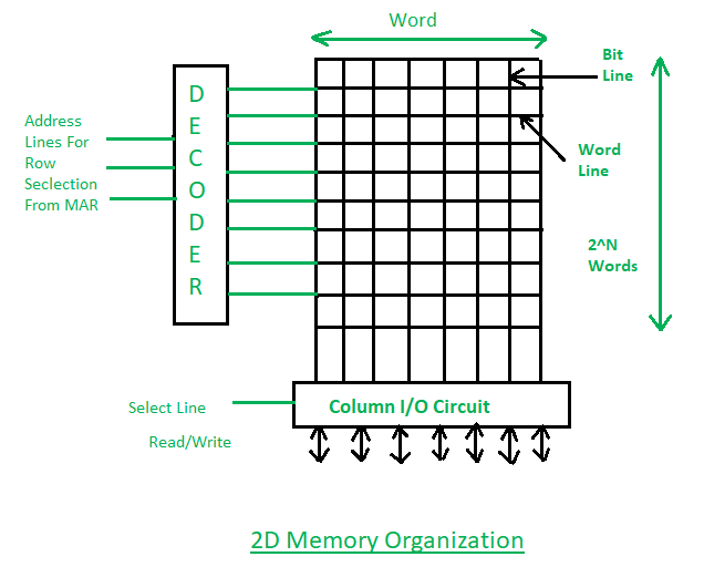
2D Memory Organization has following properties:
1. Basically in 2D organization memory is divides in the form of rows and columns.
2. Each row contains a word now in this memory organization there is a decoder.
3. A decoder is a combinational circuit which contains n input lines and 2n output lines. One of the output line will select the row which address is contained in the MAR.
4. And the word which is represented by the row that will get selected and either read or write through the data lines.
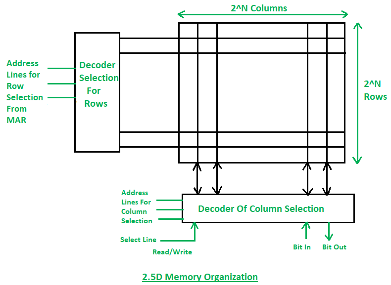
2.5D Memory Organization has following properties:
1. In 2.5D Organization the scenario is the same but we have two different decoders one is column decoder and another is row decoder.
2. Column decoder used to select the column and row decoder is used to select the row. Address from the MAR will go in decoders’ input. Decoders will select the respective cell.
3. Through the bit outline, the data from that location will be read or through the bit in line data will be written at that memory location.
Comparison between 2D & 2.5D Organizations:
1. In 2D organization hardware is fixed but in 2.5D hardware changes.
2. 2D Organization requires more no. Of Gates while 2.5D requires less no. Of Gates.
3. 2D is more complex in comparison to the 2.5D Organization.
4. Error correction is not possible in the 2D organization but In 2.5D error correction is easy.
5. 2D is more difficult to fabricate in comparison to the 2.5D organization.
What is ROM?
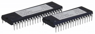
Fig - ROM
ROM, which stands for read only memory, is a memory device or storage medium that stores information permanently. It is also the primary memory unit of a computer along with the random access memory (RAM). It is called read only memory as we can only read the programs and data stored on it but cannot write on it. It is restricted to reading words that are permanently stored within the unit.
The manufacturer of ROM fills the programs into the ROM at the time of manufacturing the ROM. After this, the content of the ROM can't be altered, which means you can't reprogram, rewrite, or erase its content later. However, there are some types of ROM where you can modify the data.
ROM contains special internal electronic fuses that can be programmed for a specific interconnection pattern (information). The binary information stored in the chip is specified by the designer and then embedded in the unit at the time of manufacturing to form the required interconnection pattern (information). Once the pattern (information) is established, it stays within the unit even when the power is turned off. So, it is a non-volatile memory as it holds the information even when the power is turned off, or you shut down your computer.
The information is added to a RAM in the form of bits by a process known as programming the ROM as bits are stored in the hardware configuration of the device. So, ROM is a Programmable Logic Device (PLD).
A simple example of ROM is the cartridge used in video game consoles that allows the system to run many games. The data which is stored permanently on personal computers and other electronic devices like smartphones, tablets, TV, AC, etc. is also an example of ROM.
For example, when you start your computer, the screen does not appear instantly. It takes time to appear as there are startup instructions stored in ROM which are required to start the computer during the booting process. The work of the booting process is to start the computer. It loads the operating system into the main memory (RAM) installed on your computer. The BIOS program, which is also present in the computer memory (ROM) is used by the microprocessor of the computer to start the computer during the booting process. It allows you to open the computer and connects the computer with the operating system.
ROM is also used to store Firmware, which is a software program which remains attached to the hardware or programmed on a hardware device like a keyboard, hard drive, video cards, etc. It is stored in the flash ROM of a hardware device. It provides instructions to the device to communicate and interact with other devices.
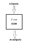
Fig - Block Diagram of ROM
The block of ROM has 'n' input lines and 'm' output lines. Each bit combination of the input variables is known as an address. Each bit combination that comes out through output lines is called a word. The number of bits per word is equal to the number of output lines, m.
The address of a binary number refers to one of the addresses of n variables. So, the number of possible addresses with 'n' input variables is 2n. An output word has a unique address, and as there are 2n distinct addresses in a ROM, there are 2n separate words in the ROM. The words on the output lines at a given time depends on the address value applied to the input lines.
Internal Structure of ROM:
The internal structure comprises two basic components: decoder and OR gates. A decoder is a circuit that decodes an encoded form (such as binary coded decimal, BCD) to a decimal form. So, the input is in binary form, and the output is its decimal equivalent. All the OR gates present in the ROM will have outputs of the decoder as their output. Let us take an example of 64 x 4 ROM. The structure is shown in the following image.
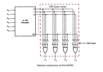
Fig–Internal construction
This Read Only Memory consists of 64 words of 4 bits each. So, there would be four output lines, and one of the 64 words available on the output lines is determined from the six input lines as we have only six inputs because in this ROM we have 26 = 64, so we can specify 64 addresses or minterms. For each address input, there is a unique selected word. For example, if the input address is 000000, word number 0 will be selected and applied to the output lines. If the input address is 111111, word number 63 is selected and applied to the output lines.
Types of ROM:
1) Masked Read Only Memory (MROM):
It is the oldest type of read only memory (ROM). It has become obsolete so it is not used anywhere in today's world. It is a hardware memory device in which programs and instructions are stored at the time of manufacturing by the manufacturer. So it is programmed during the manufacturing process and can't be modified, reprogrammed, or erased later.
The MROM chips are made of integrated circuits. Chips send a current through a particular input-output pathway determined by the location of fuses among the rows and columns on the chip. The current has to pass along a fuse-enabled path, so it can return only via the output the manufacturer chooses. This is the reason the rewriting and any other modification is not impossible in this memory.
2) Programmable Read Only Memory (PROM):
PROM is a blank version of ROM. It is manufactured as blank memory and programmed after manufacturing. We can say that it is kept blank at the time of manufacturing. You can purchase and then program it once using a special tool called a programmer.
In the chip, the current travels through all possible pathways. The programmer can choose one particular path for the current by burning unwanted fuses by sending a high voltage through them. The user has the opportunity to program it or to add data and instructions as per his requirement. Due to this reason, it is also known as the user-programmed ROM as a user can program it.
To write data onto a PROM chip; a device called PROM programmer or PROM burner is used. The process or programming a PROM is known as burning the PROM. Once it is programmed, the data cannot be modified later, so it is also called as one-time programmable device.
Uses: It is used in cell phones, video game consoles, medical devices, RFID tags, and more.
3) Erasable and Programmable Read Only Memory (EPROM):
EPROM is a type of ROM that can be reprogramed and erased many times. The method to erase the data is very different; it comes with a quartz window through which a specific frequency of ultraviolet light is passed for around 40 minutes to erase the data. So, it retains its content until it is exposed to the ultraviolet light. You need a special device called a PROM programmer or PROM burner to reprogram the EPROM.
Uses: It is used in some micro-controllers to store program, e.g., some versions of Intel 8048 and the Freescale 68HC11.
4) Electrically Erasable and Programmable Read Only Memory (EEPROM):
ROM is a type of read only memory that can be erased and reprogrammed repeatedly, up to 10000 times. It is also known as Flash EEPROM as it is similar to flash memory. It is erased and reprogrammed electrically without using ultraviolet light. Access time is between 45 and 200 nanoseconds.
The data in this memory is written or erased one byte at a time; byte per byte, whereas, in flash memory data is written and erased in blocks. So, it is faster than EEPROM. It is used for storing a small amount of data in computer and electronic systems and devices such as circuit boards.
Uses: The BIOS of a computer is stored in this memory.
5) FLASH ROM:
It is an advanced version of EEPROM. It stores information in an arrangement or array of memory cells made from floating-gate transistors. The advantage of using this memory is that you can delete or write blocks of data around 512 bytes at a particular time. Whereas, in EEPROM, you can delete or write only 1 byte of data at a time. So, this memory is faster than EEPROM.
It can be reprogrammed without removing it from the computer. Its access time is very high, around 45 to 90 nanoseconds. It is also highly durable as it can bear high temperature and intense pressure.
Uses: It is used for storage and transferring data between a personal computer and digital devices. It is used in USB flash drives, MP3 players, digital cameras, modems and solid-state drives (SSDs). The BIOS of many modern computers are stored on a flash memory chip, called flash BIOS.
Key takeaways
- ROM, which stands for read only memory, is a memory device or storage medium that stores information permanently. It is also the primary memory unit of a computer along with the random-access memory (RAM). It is called read only memory as we can only read the programs and data stored on it but cannot write on it. It is restricted to reading words that are permanently stored within the unit.
- The manufacturer of ROM fills the programs into the ROM at the time of manufacturing the ROM. After this, the content of the ROM can't be altered, which means you can't reprogram, rewrite, or erase its content later. However, there are some types of ROM where you can modify the data.
- Cache memories are small, fast SRAM based memories managed automatically in hardware.
- It is placed between two levels of memory hierarchy, to bridge the gaps in access times between processor and main memory and between main memory and disk.
- It prefetch data into cache before the processor needs it.
- Transfer between main memory and cache is in unit of blocks and implements spatial locality.
- Transfer between cache memory and registers is in units of words.

Fig: Cache Memory Design
Cache Memory principle
- If data sought is not present in cache, a block of memory of fixed size is read in to the cache.
- Locality of reference makes it likely that other words in the same block will be accessed soon.
Working of cache
- Temporal locality (locality in time): If an item is referenced, it will tend to be referenced again soon
- Spatial locality (locality in space): If an item is referenced, items whose address are close by tend to be referenced soon
Mapping Function:
- Mapping function determines how memory blocks are mapped to cache lines; different types of mapping process are:
Direct Mapping:
- The simplest technique, known as direct mapping, maps each block of main memory into only one possible cache line.
- In Direct mapping, assigned each memory block to a specific line in the cache. If a line is previously taken up by a memory block when a new block needs to be loaded, the old block is trashed.
- An address space is split into two parts index field and a tag field. The cache is used to store the tag field whereas the rest is stored in the main memory.
- Direct mappings performance is directly proportional to the Hit ratio.
- For purposes of cache access, each main memory address can be viewed as consisting of three fields. The least significant w bits identify a unique word or byte within a block of main memory. In most contemporary machines, the address is at the byte level. The remaining s bits specify one of the 2s blocks of main memory.
- The cache logic interprets these s bits as a tag of s-r bits (most significant portion) and a line field of r bits. This latter field identifies one of the m=2r lines of the cache.
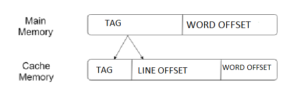
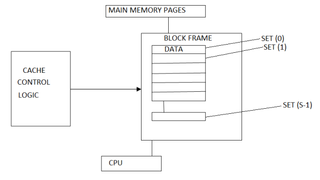
Figure 5 Direct Mapping Process
Associative Mapping:
- The associative memory is used to store content and addresses of the memory word.
- Any block can go into any line of the cache i.e that the word id bits are used to identify which word in the block is needed, but the tag becomes all of the remaining bits.
- It is considered to be the fastest and the most flexible mapping form.
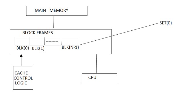
Fig: Associative Mapping
Set Associative Mapping:
- Set associative memory is an enhanced form of direct mapping; it removes the drawback of direct mapping.
- Set associative addresses the problem of thrashing in the direct mapping method, it does this by saying that instead of having exactly one line that a block can map to in the cache, will group a few lines together creating a set.
- Then a block in memory can map to any one of the lines of a specific set. Set-associative mapping allows that each word that is present in the cache can have two or more words in the main memory for the same index address.

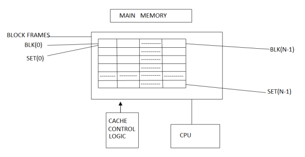
Figure: Set Associative Mapping
Key takeaway
- Cache memories are small, fast SRAM based memories managed automatically in hardware.
- It is placed between two levels of memory hierarchy, to bridge the gaps in access times between processor and main memory and between main memory and disk.
- It prefetch data into cache before the processor needs it.
- Transfer between main memory and cache is in unit of blocks and implements spatial locality.
Cache memory bridges the speed mismatch between the processor and the main memory.
When cache hit occurs,
- The required word is present in the cache memory.
- The required word is delivered to the CPU from the cache memory.
When cache miss occurs,
- The required word is not present in the cache memory.
- The page containing the required word has to be mapped from the main memory.
- This mapping is performed using cache mapping techniques.
In this article, we will discuss different cache mapping techniques.
Cache Mapping-
- Cache mapping defines how a block from the main memory is mapped to the cache memory in case of a cache miss.
OR
- Cache mapping is a technique by which the contents of main memory are brought into the cache memory.
The following diagram illustrates the mapping process-
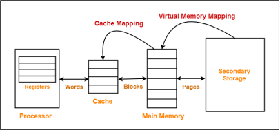
Fig – Mapping process
Now, before proceeding further, it is important to note the following points-
NOTES
- Main memory is divided into equal size partitions called as blocks or frames.
- Cache memory is divided into partitions having same size as that of blocks called as lines.
During cache mapping, block of main memory is simply copied to the cache and the block is not actually brought from the main memory.
Cache Mapping Techniques-
Cache mapping is performed using following three different techniques-

- Direct Mapping
- Fully Associative Mapping
- K-way Set Associative Mapping
1. Direct Mapping-
In direct mapping,
- A particular block of main memory can map only to a particular line of the cache.
- The line number of cache to which a particular block can map is given by-
Cache line number
= (Main Memory Block Address) Modulo (Number of lines in Cache)
Example-
- Consider cache memory is divided into ‘n’ number of lines.
- Then, block ‘j’ of main memory can map to line number (j mod n) only of the cache.
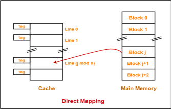
Fig – Direct mapping
Need of Replacement Algorithm-
In direct mapping,
- There is no need of any replacement algorithm.
- This is because a main memory block can map only to a particular line of the cache.
- Thus, the new incoming block will always replace the existing block (if any) in that particular line.
Division of Physical Address-
In direct mapping, the physical address is divided as-
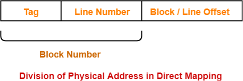
Fig – Physical address
2. Fully Associative Mapping-
In fully associative mapping,
- A block of main memory can map to any line of the cache that is freely available at that moment.
- This makes fully associative mapping more flexible than direct mapping.
Example-
Consider the following scenario-
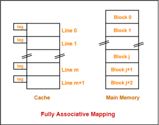
Fig – Fully associative mapping
Here,
- All the lines of cache are freely available.
- Thus, any block of main memory can map to any line of the cache.
- Had all the cache lines been occupied, then one of the existing blocks will have to be replaced.
Need of Replacement Algorithm-
In fully associative mapping,
- A replacement algorithm is required.
- Replacement algorithm suggests the block to be replaced if all the cache lines are occupied.
- Thus, replacement algorithm like FCFS Algorithm, LRU Algorithm etc is employed.
Division of Physical Address-
In fully associative mapping, the physical address is divided as-

Fig – Physical address
3. K-way Set Associative Mapping-
In k-way set associative mapping,
- Cache lines are grouped into sets where each set contains k number of lines.
- A particular block of main memory can map to only one particular set of the cache.
- However, within that set, the memory block can map any cache line that is freely available.
- The set of the cache to which a particular block of the main memory can map is given by-
Cache set number
= (Main Memory Block Address) Modulo (Number of sets in Cache)
Example-
Consider the following example of 2-way set associative mapping-
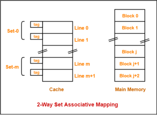
Fig – 2-way set associative mapping
Here,
- k = 2 suggests that each set contains two cache lines.
- Since cache contains 6 lines, so number of sets in the cache = 6 / 2 = 3 sets.
- Block ‘j’ of main memory can map to set number (j mod 3) only of the cache.
- Within that set, block ‘j’ can map to any cache line that is freely available at that moment.
- If all the cache lines are occupied, then one of the existing blocks will have to be replaced.
Need of Replacement Algorithm-
- Set associative mapping is a combination of direct mapping and fully associative mapping.
- It uses fully associative mapping within each set.
- Thus, set associative mapping requires a replacement algorithm.
Division of Physical Address-
In set associative mapping, the physical address is divided as-

Fig – Physical address
Special Cases-
- If k = 1, then k-way set associative mapping becomes direct mapping i.e.
1-way Set Associative Mapping ≡ Direct Mapping
- If k = Total number of lines in the cache, then k-way set associative mapping becomes fully associative mapping.
Key takeaway
Cache Mapping-
- Cache mapping defines how a block from the main memory is mapped to the cache memory in case of a cache miss.
- Cache mapping is a technique by which the contents of main memory are brought into the cache memory.
Auxiliary Memory
An Auxiliary memory is known as the lowest-cost, highest-capacity and slowest-access storage in a computer system. It is where programs and data are kept for long-term storage or when not in immediate use. The most common examples of auxiliary memories are magnetic tapes and magnetic disks.
Magnetic Disks
A magnetic disk is a type of memory constructed using a circular plate of metal or plastic coated with magnetized materials. Usually, both sides of the disks are used to carry out read/write operations. However, several disks may be stacked on one spindle with read/write head available on each surface.
The following image shows the structural representation for a magnetic disk.
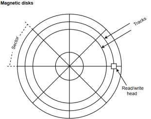
Figure – Magnetic disks
The memory bits are stored in the magnetized surface in spots along the concentric circles called tracks.
The concentric circles (tracks) are commonly divided into sections called sectors.
Magnetic Tape
Magnetic tape is a storage medium that allows data archiving, collection, and backup for different kinds of data. The magnetic tape is constructed using a plastic strip coated with a magnetic recording medium.
The bits are recorded as magnetic spots on the tape along several tracks. Usually, seven or nine bits are recorded simultaneously to form a character together with a parity bit.
Magnetic tape units can be halted, started to move forward or in reverse, or can be rewound. However, they cannot be started or stopped fast enough between individual characters. For this reason, information is recorded in blocks referred to as records.
Optical disks
An optical disk is any computer disk that uses optical storage techniques and technology to read and write data. It is a storage device in which optical (light) energy is used. It is a computer storage disk that stores data digitally and uses laser beams to read and write data. It uses the optical technology in which laser light is centred to the spinning disks.
Difference Between Magnetic Disk and Optical Disk.
S.NO. | MAGNETIC DISK | OPTICAL DISK |
1 | Media type used is Multiple fixed disk | Media type used is Single removable disk |
2 | Intermediate signal to noise ratio | Excellent signal to noise ratio |
3 | Sample rate is Low | Sample rate is High |
4 | Implemented where data is randomly accessed. | Implemented in streaming files. |
5 | Only one disk can be used at a time | Mass replication is possible |
6 | Tracks in the magnetic disk are generally circular | In optical disk the tracks are constructed spirally. |
7 | The data in the magnetic disk is randomly accessed. | In the optical disk, the data is sequentially accessed. |
8 | In the magnetic disk, only one disk is accessed at a time. | Optical disk allows mass replication |
A computer can address more memory than the amount physically installed on the system. This extra memory is actually called virtual memory and it is a section of a hard disk that's set up to emulate the computer's RAM.
The main visible advantage of this scheme is that programs can be larger than physical memory. Virtual memory serves two purposes. First, it allows us to extend the use of physical memory by using disk. Second, it allows us to have memory protection, because each virtual address is translated to a physical address.
Following are the situations, when entire program is not required to be loaded fully in main memory.
- User written error handling routines are used only when an error occurred in the data or computation.
- Certain options and features of a program may be used rarely.
- Many tables are assigned a fixed amount of address space even though only a small amount of the table is actually used.
- The ability to execute a program that is only partially in memory would counter many benefits.
- Less number of I/O would be needed to load or swap each user program into memory.
- A program would no longer be constrained by the amount of physical memory that is available.
- Each user program could take less physical memory, more programs could be run the same time, with a corresponding increase in CPU utilization and throughput.
Modern microprocessors intended for general-purpose use, a memory management unit, or MMU, is built into the hardware. The MMU's job is to translate virtual addresses into physical addresses. A basic example is given below −
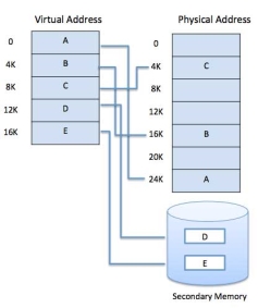
Fig – Memory Address
Virtual memory is commonly implemented by demand paging. It can also be implemented in a segmentation system. Demand segmentation can also be used to provide virtual memory.
Demand Paging
A demand paging system is quite similar to a paging system with swapping where processes reside in secondary memory and pages are loaded only on demand, not in advance. When a context switch occurs, the operating system does not copy any of the old program’s pages out to the disk or any of the new program’s pages into the main memory Instead, it just begins executing the new program after loading the first page and fetches that program’s pages as they are referenced.
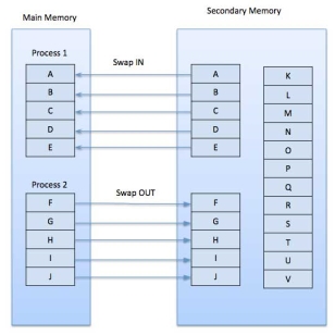
Fig – Swap in swap out
While executing a program, if the program references a page which is not available in the main memory because it was swapped out a little ago, the processor treats this invalid memory reference as a page fault and transfers control from the program to the operating system to demand the page back into the memory.
Advantages
Following are the advantages of Demand Paging −
- Large virtual memory.
- More efficient use of memory.
- There is no limit on degree of multiprogramming.
Disadvantages
- Number of tables and the amount of processor overhead for handling page interrupts are greater than in the case of the simple paged management techniques.
Page Replacement Algorithm
Page replacement algorithms are the techniques using which an Operating System decides which memory pages to swap out, write to disk when a page of memory needs to be allocated. Paging happens whenever a page fault occurs and a free page cannot be used for allocation purpose accounting to reason that pages are not available or the number of free pages is lower than required pages.
When the page that was selected for replacement and was paged out, is referenced again, it has to read in from disk, and this requires for I/O completion. This process determines the quality of the page replacement algorithm: the lesser the time waiting for page-ins, the better is the algorithm.
A page replacement algorithm looks at the limited information about accessing the pages provided by hardware, and tries to select which pages should be replaced to minimize the total number of page misses, while balancing it with the costs of primary storage and processor time of the algorithm itself. There are many different page replacement algorithms. We evaluate an algorithm by running it on a particular string of memory reference and computing the number of page faults,
Reference String
The string of memory references is called reference string. Reference strings are generated artificially or by tracing a given system and recording the address of each memory reference. The latter choice produces a large number of data, where we note two things.
- For a given page size, we need to consider only the page number, not the entire address.
- If we have a reference to a page p, then any immediately following references to page p will never cause a page fault. Page p will be in memory after the first reference; the immediately following references will not fault.
- For example, consider the following sequence of addresses − 123,215,600,1234,76,96
- If page size is 100, then the reference string is 1,2,6,12,0,0
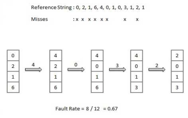
First In First Out (FIFO) algorithm
- Oldest page in main memory is the one which will be selected for replacement.
- Easy to implement, keep a list, replace pages from the tail and add new pages at the head.
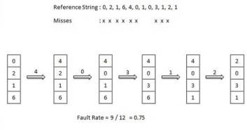
Optimal Page algorithm
- An optimal page-replacement algorithm has the lowest page-fault rate of all algorithms. An optimal page-replacement algorithm exists, and has been called OPT or MIN.
- Replace the page that will not be used for the longest period of time. Use the time when a page is to be used.
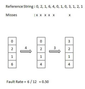
Least Recently Used (LRU) algorithm
- Page which has not been used for the longest time in main memory is the one which will be selected for replacement.
- Easy to implement, keep a list, replace pages by looking back into time.
Page Buffering algorithm
- To get a process start quickly, keep a pool of free frames.
- On page fault, select a page to be replaced.
- Write the new page in the frame of free pool, mark the page table and restart the process.
- Now write the dirty page out of disk and place the frame holding replaced page in free pool.
Least frequently Used (LFU) algorithm
- The page with the smallest count is the one which will be selected for replacement.
- This algorithm suffers from the situation in which a page is used heavily during the initial phase of a process, but then is never used again.
Most frequently Used (MFU) algorithm
- This algorithm is based on the argument that the page with the smallest count was probably just brought in and has yet to be used.
Key takeaways
- A computer can address more memory than the amount physically installed on the system. This extra memory is actually called virtual memory and it is a section of a hard disk that's set up to emulate the computer's RAM.
- The main visible advantage of this scheme is that programs can be larger than physical memory. Virtual memory serves two purposes. First, it allows us to extend the use of physical memory by using disk. Second, it allows us to have memory protection, because each virtual address is translated to a physical address.
References:
1. Computer System Architecture - M. Mano
2. Carl Hamacher, Zvonko Vranesic, Safwat Zaky Computer Organization, McGraw-Hill, Fifth Edition, Reprint 2012
3. John P. Hayes, Computer Architecture and Organization, Tata McGraw Hill, Third Edition, 1998. Reference books
4. William Stallings, Computer Organization and Architecture-Designing for Performance, Pearson Education, Seventh edition, 2006.
5. Behrooz Parahami, “Computer Architecture”, Oxford University Press, Eighth Impression, 2011.