Unit-2
Pin diagram and internal architecture of 8085 microprocessor
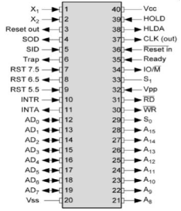
Pin diagram
- Address bus A15-A8.
- Data bus AD7-AD0.
- Three control signals are RD, WR & ALE.
- RD: It indicates that the selected IO or memory device can be read and is ready to accept data available on the data bus.
- WR: It indicates that the data on the data bus can be written into a selected memory or IO location.
- ALE: It is a positive going pulse that is generated when a new operation is started by the microprocessor. When high, it indicates address and when low, it indicates data.
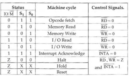
- Three status signals are IO/M, S0 & S1.
 IO/M: It is used for input/output or memory selection i.e when it is high it indicates IO operation and when it is low then it indicates memory operation.
 - S1 & S0: They are used to identify the type of current operation.
- Power supply: VCC & VSS.
- VCC: +5V and VSS : ground signal (0V).
- Clock signals: There are 3 types of clock signals, X1, X2 and CLK OUT.
- X1, X2: A crystal (RC, LC N/W) is connected at these two pins and is used to set frequency of the internal clock generator. This frequency is internally divided by 2.
|
Fig.1: Pin diagram of 8085 (ref 1)
- CLK OUT: This signal is used as the system clock for devices connected with the microprocessor.
- Interrupts are the signals generated by external devices requesting the microprocessor to perform a certain task. There are 5 types of interrupt. They are TRAP, RST 7.5, RST 6.5, RST 5.5, and INTR.
- INTA: It is an interrupt acknowledge signal.
- RESET IN: It is used to reset the microprocessor by setting the program counter to zero.
- RESET OUT: It is used to reset all the devices connected to the microprocessor when microprocessor is reset.
- READY: It indicates that the device is ready to send or receive data. If it is low, then the CPU has to wait for it to go high.
- HOLD: It indicates that another master is requesting the use of the address and data buses.
- HLDA: It stands for HOLD Acknowledge. It indicates that the CPU has received the HOLD request and is ready to share the bus in the next clock cycle. After the HOLD signal is removed HLDA is set to low.
- SID and SOD signals are used for serial communication.
- SOD (Serial output data line): It is set/reset by the SIM instruction.
- SID (Serial input data line): when it is active, the data on this line is loaded into accumulator whenever a RIM instruction is executed.
Architecture of 8085 microprocessor
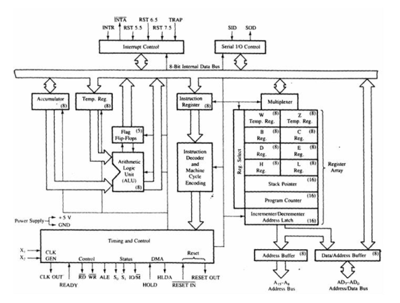
It includes the timing & control unit, Arithmetic and logic unit, decoder, instruction register, interrupt control, a register array, serial input/output control and the central processing unit.
It performs all arithmetical and logical operations like add, subtract, AND, OR etc. The temporary registers and accumulators hold the information throughout the operations and the result is stored in the accumulator. The different flags are arranged or rearranged on the basis of result.
Flag Registers
It is an 8 bit register. They are of five types namely sign, zero, auxiliary carry, parity and carry.
Control and Timing Unit
It coordinates with all the processes of the microprocessor by the clock and provides the control signals required for communication between the microprocessor and peripherals. It is used to control the internal as well as external circuits.
- Decoder and Instruction Register
when an order is received from memory which is located in the instruction register, it is encoded & decoded into various device cycles.
Register Array
The general-purpose registers are classified into several types such as B, C, D, E, H, & L. They are 8-bit registers. The register pairs are BC, DE & HL.
- Special Purpose Registers
These registers are of four types namely program counter, stack pointer, increment or decrement register, address or data buffer.
Program Counter
It is a 16 bit register. It is used to store data, memory information etc. whenever memory is incremented, the PC then points to the next location.
Stack Pointer
It is a 16 bit register. It always points to stack which can be incremented or decremented by PUSH and POP instruction.
Increment or Decrement Register
It is an 8-bit register which can be increased or decreased by one. It is useful for incrementing or decrementing program counters as well as stack pointer register content with one. This operation can be done on any memory location or any kind of register.
Address Bus and Data Bus
Data bus carries the data required to be stored. It is bidirectional. Address bus carries the location to where the data should be stored and it is unidirectional. It is used to transfer the data & address.
|
Fig.2: Architecture of 8085 (ref 1)
Key takeaway
It is 8-bit microprocessor. It has 40 pins. It includes the timing & control unit, Arithmetic and logic unit, decoder, instruction register, interrupt control, a register array, serial input/output control and the central processing unit.
Register Organisation
|
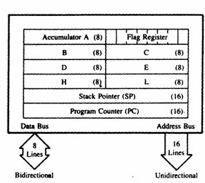
Fig 3 Register organisation of 8085
A=Accumulator
SP = Stack Pointer
PC =Program Counter
Flag Register
|

Register Pairs
There are three register pairs BC, DE and HL. Where HL is special register pair as it points current location of memory.
Stack Pointer (SP):
It holds address. It is important to initialise SP before using the stack. It is initialised by the highest memory location.
Program Counter (PC)
It will always hold the address. It sequences the execution of instructions. The microprocessor is a sequential logic device.
ALU
The word length of ALU depends upon of an internal data bus.
It is 8 bit and is always controlled by timing and control circuits.
It provides status or result of flag register.
|
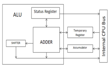
Fig 4 ALU of 8085
Adder: It performs arithmetic operations like addition, subtraction, increment, decrement, etc. The result of operation is stored into accumulator.
Shifter: It performs logical operations like rotate left, rotate right, etc. The result of operation is again stored into accumulator.
Status Register: Also known as flag register. It contains a no. of flags either to indicate conditions arising after last ALU operation or to control certain operations.
Accumulator:
It is one of the general-purpose registers of microprocessor also called as A register.
The accumulator is an 8-bit register that is a part of arithmetic/logic unit (ALU).
This register is used to store 8-bit data and to perform arithmetic and logical operations.
The result of an operation is stored in the accumulator.
The user can access this register by giving appropriate instructions (commands).
Temporary Register:
It is also called as operand register (8 bit).
It provides operands to ALU. ALU can store immediate result in temporary register.
It is not accessible by user.
Status or flag register:
|
Flag register is a group of flip flops used to give status of different operations result.
The flag register is connected to ALU.
Once an operation is performed by ALU the result is transferred on internal data bus and status of result will be stored in flip flops.
They are called Zero (Z), Carry (CY), Sign (S), Parity (P), and Auxiliary Carry (AC) flags.
Control and Status Signal
- ALE – It is an Address Latch Enable signal. It goes high during first T state of a machine cycle and enables the lower 8-bits of the address, if its value is 1 otherwise data bus is activated.
- IO/
 – It is a status signal which determines whether the address is for input-output or memory. When it is high(1) the address on the address bus is for input-output devices. When it is low(0) the address on the address bus is for the memory.
 - SO, S1 – These are status signals. They distinguish the various types of operations such as halt, reading, instruction fetching or writing.
 – It is a signal to control READ operation. When it is low the selected memory or input-output device is read.
 – It is a signal to control WRITE operation. When it goes low the data on the data bus is written into the selected memory or I/O location.
- READY – It senses whether a peripheral is ready to transfer data or not. If READY is high(1) the peripheral is ready. If it is low(0) the microprocessor waits till it goes high. It is useful for interfacing low speed devices.
Interrupts
The 8085 has five interrupt signals that can be used to interrupt a program execution.
INTR
RST 7.5
RST 6.5
RST 5.5
TRAP
The microprocessor acknowledges Interrupt Request by INTA’ signal. In addition to Interrupts, there are three externally initiated signals namely RESET, HOLD and READY. To respond to HOLD request, it has one signal called HLDA.
- INTR – It is an interrupt request signal.
 – It is an interrupt acknowledgment sent by the microprocessor after INTR is received.
Machine Cycle
|
Key takeaway
The word length of ALU depends upon of an internal data bus. It is 8 bit and is always controlled by timing and control circuits. It provides status or result of flag register. The microprocessor acknowledges Interrupt Request by INTA’ signal. In addition to Interrupts, there are three externally initiated signals namely RESET, HOLD and READY. To respond to HOLD request, it has one signal called HLDA.
Instruction sets refer section 2.5
Addressing modes
The instructions are used to transfer the data from one register to another register, from the memory to the register, and from the register to the memory without any change in the content.
Addressing modes in 8085 is divided into 5 groups −
Here, the 8/16-bit data is specified in the instruction itself as one of its operands. For example: MVI B, 40F means 40F is copied into register B.
Here, the data is copied from one register to another.
For example: MOV B, A: means data in register A is copied to register B.
Here, the data is directly copied from the given address to the register.
For example: LDB 5008H: means the data at address 5008H is copied to register B.
Here, the data is transferred from one register to another by using the address pointed by the register.
For example: MOV B, K: means data is transferred from the memory address pointed by the register K to the register B.
Here, it doesn’t require any operand; the data is specified by the opcode itself.
For example: CMP.
Key takeaway
There are 5 addressing modes register, direct, indirect, implied and immediate modes.
The total amount of memory required to feed the instruction in memory is called as Instruction word size. 8085 microprocessors can accommodate 8-bit data and to store 16-bit data, two consecutive memory locations are used.
According to the instruction word size, there are three types of instructions. They are:
- 1 byte instruction
- They include opcode and operand in the same byte.
- Operand are internal registers and coded into the instruction.
- Instruction requires one memory location to store one single byte of memory.
- For example:
MOV B,C
HLT
- 2 byte instruction
- Here 1st byte specifies opcode and the 2nd byte species operand.
- Instruction requires two memory location to store in memory.
- For example:
MOV B,20H
IN 25H
- 3 byte instruction
- Here 1st byte is opcode and the next two bytes species memory address.
- The 2nd byte holds the lower order address and the 3rd byte holds the higher order address.
- Instructions require three memory locations to store in memory.
- For example:
LDA 2000H
JMP 5055H
Key takeaway
The instructions can be classified on the size i.e number of bytes. There are 1-byte, 2-byte and 3-byte instructions.
2.5.1 Data Transfer Instruction
OPCODE | OPERAND | DESCRIPTION |
MOV | Rd, Rs Rd, M M, Rs | Transfer the contents of the source to the destination. |
MVI | Rd, data M, data | Move immediate data into the destination register |
LXI | Reg. pair, data | Move 16 bit data into the register pair |
LDA | 16 bit address | Load accumulator with data present at the specified address |
XCHG | - | Exchange the contents of HL with DE |
For example: MOV B, C
MVI B, 20H
LXI H, 4020H
LDA 6000H
2.5.2 Arithmetic Instructions
These instructions perform the operations like:
• Addition
• Subtraction
• Increment
• Decrement
OPCODE | OPERAND | DESCRIPTION |
ADD | R M | Add the contents of register with the contents of accumulator and save in accumulator. |
ADC | R M | Add the contents of register with the contents of accumulator with carry and save in accumulator. |
ADI | 8 bit data | Add data with the content of acc |
DAD | Reg pair | Add register pair to H-L pair |
SUB | R M | Subtract the contents of register with the contents of accumulator and save in accumulator. |
SBB | R M | Subtract the contents of register with borrow from the contents of accumulator and save in accumulator. |
SUI | 8 bit data | Subtract data with the content of acc |
INR | R M | Increment register or memory by 1 |
DCR | R M | Decrement register or memory by 1 |
For example: ADD C
ADC M
ADI 40H
DAD HL
SUB B
SUI 20H
INR C
2.5.3 Logical Instructions
The logical operations are:
• AND • OR • XOR • Rotate • Compare • Complement
OPCODE | OPERAND | DESCRIPTION |
CMP | R M | Compare the contents of register or memory with accumulator |
ANA | R M | Logical AND the contents of register with accumulator |
ANI | 8 bit data | Logical AND the data with accumulator |
XRA | R M | XOR the contents of register with accumulator |
ORA | R M | Logical OR the contents of register with accumulator |
RLC | - | Rotate accumulator left |
RRC | - | Rotate accumulator right |
CMA | - | Complement accumulator |
For example: CMP C
ANA B
ANI 40H
XRA M
ORA C
RLC
2.5.4 Branching Instructions
These instructions alter the normal sequential flow conditionally or unconditionally.
OPCODE | OPERAND | DESCRIPTION |
JMP | 16 bit address | Jump unconditionally to the given location |
JC | 16 bit address | Jump if carry |
JNC | 16 bit address | Jump if no carry |
JZ | 16 bit address | Jump if zero |
JNZ | 16 bit address | Jump if no zero |
CALL | 16 bit address | Call unconditionally |
RET | - | Return unconditionally |
RST | 0-7 | Restart (Software Interrupts) |
For example: JMP 2000H
RET
RST 6
2.5.5 Machine Control Instructions
They control machine functions and they are HALT, interrupt etc.
2.5.6 Assembler Directives
They convert assembly language program to machine language. The basic aim of the assemble directive are to sow the beginning and end of program. They give storage location for data. They also define the start and end of different segments.
They are also called as pseudo-opcode. These instructions are neither translated into machine code nor assigned any memory location in the object file. Some of the important assembler directives for an assembler or a cross assembler are listed and described here.
Data -Bytes (Data Bytes): Assemble bytes of data are stored in successive memory location until all values are stored. This is a convenient way of writing a data string.
Exapmle-1
If we do not use
LDA, 4150H
MOV B,A
Or
MVI B, 25H
MOV A, B
We use DB, 25H, 29H
Data Word (DB)
It is used to just initialise an area of 2 bytes at a time. For example: DW 2050H
Data Quard Word (DQ)
It initialises 4 word or 8-bits in one instruction that means we take word which occupy a 8-bit number of decimal. For example: DQ 2050 95 76 30 75 95 86 H
Definite 10 Bit (DT)
It is similar to DQ but it occupies 2 bits extra. For example: DT 1 2 3 4 5 6 7 8 9 0 1 2 3 4 5 6 7 8 9 AB H.
Define Double Word (DD)
It is similar to DQ and DT. For example: DD 2050 60 75H
Definite Storage Location (DS)
Reserves a specified number of memory locations. In this example four memory locations are reserved for OUTBUF. For example: OUTBUF DS4
ORG
If we use ORG 4000H that means the next block of instructions should be stored in memory location starting 4000H.
EQU (equate)
Generally, we transfer any information in port address. Instead of
MVI A, 09H
OUT PA
PA EQU 40H
END
It is similar to HALT. But the HLT suggest the end of program but that does not necessarily mean it is the end of the assembly.
Key takeaway
Instructions are the codes given to the microprocessor by the user in order to perform various operations. They can be arithmetical, logical, machine control etc.
Reference:
1. Gaonkar, Ramesh S , “Microprocessor Architecture, Programming and Applications with 8085”, Penram International Publishing.
2. Ray A K, Bhurchandi K M, “Advanced Microprocessors and Peripherals”, TMH Hall D V, Microprocessor Interfacing’, TMH
3.Liu and, “Introduction to Microprocessor”, TMH
4. Brey, Barry B, “INTEL Microprocessors”, PHI
