Unit-3
Architecture of 8086 microprocessor
3.1.1 Register Organization
- The 8086 microprocessor has a total of fourteen registers that can be used by the programmer.
- It is basically divided into four groups.
Four General purpose registers
Four Index/Pointer registers
Four Segment registers
Two Other registers
- Accumulator register consists of two 8-bit registers AL and AH. They can be used together as a 16-bit register AX. AL contains the lower order byte and AH contains the higher order byte. Accumulator can be used for both I/O operations and string manipulation.
- Base register comprises of two 8-bit registers BL and BH. They can be used together as a 16-bit register BX. BL contains the low-order byte and BH contains the high-order byte. BX register contains a data pointer used for base, base index or register indirect addressing.
- Count register comprises of two 8-bit registers CL and CH. They can be used together as a 16-bit register CX. CL register contains the low order byte and CH contains the high-order byte. It is used in Loop, shift/rotate instructions and also as a counter in string manipulation.
- Data register comprises of two 8-bit registers DL and DH. They can be used together as a 16-bit register DX. DL register contains the low order byte and DH contains the high-order byte. They can be used as a port number in I/O operations. In integer 32-bit multiplication and division instruction, the DX register contains higher order word of the resulting number.
|
Fig.1: General purpose registers
3.1.2 BUS INTERFACE UNIT (BIU)
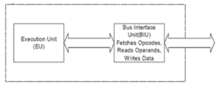
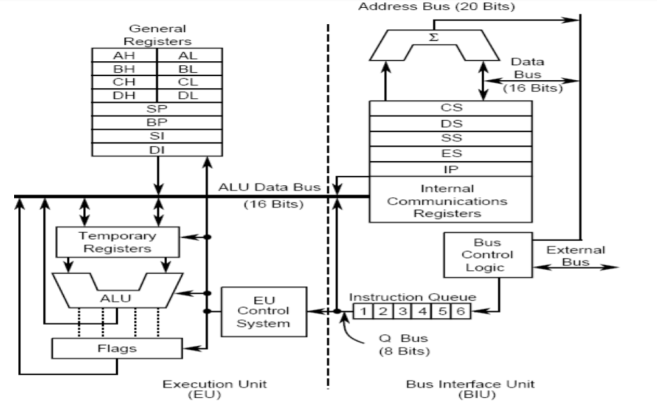
- It is a 16 bit bidirectional data bus and 20 bit address bus.
It is responsible for all external bus operations.
It performs the following functions namely Instruction fetching, Instruction queuing, Operand fetching and storage, address relocation and bus control.
- It uses a mechanism called as an instruction stream queue for implementation of a pipeline architecture.
- This queue permits pre fetching of up to six bytes of instruction code. Whenever the queue is not full, it has room for at least two more bytes. It is free to look ahead in the program by pre fetching the next sequential instruction.
- These pre fetched instructions are held in its FIFO queue. It fetches two instruction bytes in a single memory cycle.
- It shifts automatically through the FIFO to the empty location after a byte is loaded at the input end of the queue.
- The EU accesses the queue from the output end. It reads instruction byte one by one from the output of the queue. If the queue is full, the EU does not request access to operand in memory. These intervals are known as Idle state.
- When the EU request it to read or write operands from memory or I/O, the BIU is already in the process of fetching an instruction, then it first completes the instruction fetch cycle before the operand read / write cycle is initiated.
- It comprises of a dedicated adder which generates the 20 bit physical address that is output on the address bus.
- For example: The physical address to be fetched is formed by combining the current contents of the CS register and the IP register.
3.1.3 EXECUTION UNIT (EU)
- EU is used for decoding and executing all instructions.
- It extracts instructions from the top of the queue in the BIU, decodes them, generates operands passes them to the BIU and requests it to perform the read or write to memory or I/O and also performs the operation on the operands.
- At the time of execution, the EU checks and updates the status and control flags on the basis of the results of executing the instruction.
- The EU waits for the next instruction byte to be fetched and shifted to top of the queue if the queue is empty.
- It transfers control to a location when the EU executes a branch or jump instruction.
- Whenever this occurs, the BIU automatically resets the queue and begins the fetching of instructions from this new location to refill the queue.
|
Fig.2: BIU and EU
|
Fig 3: BIU and EU architecture
3.1.4 Memory Addressing
Memory addressing
- It is the main component of a computer to store temporary data and machine instructions. In a program, programmers need to read from and write into memory various locations.
- There are different forms of memory addressing modes
Direct Addressing
In this, the effective address of the memory location is written directly in the instruction.
For Example: MOV BL, [0300H]
Register indirect addressing
It allows data to be addressed at any memory location through an offset address held in any of the following registers: BP, BX, DI & SI.
For Example: MOV BX, [AX] ;
ADD CX, {AX}
Based addressing
Here, the offset address of the operand is provided by the sum of contents of the BX/BP registers and 8-bit/16-bit displacement.
For Example: MOV CX, [BX+04],
ADD DL, [BX+08]
Indexed addressing
In this, the operands offset address is generated by adding the contents of SI or DI register and 8-bit/16-bit displacements.
For Example: MOV CX, [SI+16],
ADD BL, [DI+16]
Based indexed addressing
In this, the offset address of the operand is found by summing the base register to the contents of an Index register
For Example: ADD BX, [AX+SI],
MOV CX, [AX+DI]
Based indexed with displacement
In this, the operands offset is found by adding the base register contents that is an Index registers contents and 8 or 16-bit displacement.
For Example: MOV CX, [BX+DI+08],
ADD AX, [BX+SI+16]
3.1.5 Memory Segmentation
Segmentation is the process in which the main memory of the computer is logically divided into different segments and each segment has its own base address. It is basically used to enhance the speed of execution of the computer system, so that the processor is able to fetch and execute the data from the memory easily and fast.
Need for Segmentation –
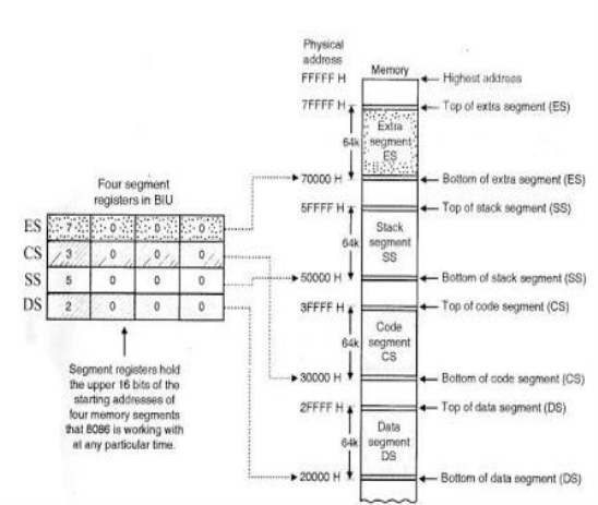
The Bus Interface Unit (BIU) contains four 16 bit special purpose registers (mentioned below) called as Segment Registers.
- Code segment register (CS): is used for addressing memory location in the code segment of the memory, where the executable program is stored.
- Data segment register (DS): points to the data segment of the memory where the data is stored.
- Extra Segment Register (ES): also refers to a segment in the memory which is another data segment in the memory.
- Stack Segment Register (SS): is used for addressing stack segment of the memory. The stack segment is that segment of memory which is used to store stack data.
The number of address lines in 8086 is 20, 8086 BIU will send 20bit address, so as to access one of the 1MB memory locations. The four segment registers actually contain the upper 16 bits of the starting addresses of the four memory segments of 64 KB each with which the 8086 is working at that instant of time. A segment is a logical unit of memory that may be up to 64 kilobytes long.
|
Fig 4 Memory Segmentation
- Overlapping Segment – A segment starts at a particular address and its maximum size can go up to 64kilobytes. But if another segment starts along with this 64kilobytes location of the first segment, then the two are said to be Overlapping Segment.
- Non-Overlapped Segment – A segment starts at a particular address and its maximum size can go up to 64kilobytes. But if another segment starts before this 64kilobytes location of the first segment, then the two segments are said to be Non-Overlapped Segment.
Rules of Segmentation
Segmentation process follows some rules as follows:
- The starting address of a segment should be such that it can be evenly divided by 16.
- Minimum size of a segment can be 16 bytes and the maximum can be 64 kB.
|
Key takeaway
Segmentation is the process in which the main memory of the computer is logically divided into different segments and each segment has its own base address.
There are basically four groups of registers:
Four General purpose registers
Four Index/Pointer registers
Four Segment registers
Two Other registers
8086 microprocessor operates in 2 modes:
- Minimum mode
- It can be selected by setting MN/MX pin to logic 1 and it acts like a single microprocessor.
- In this mode, all the control signals are provided by the microprocessor chip itself.
- Maximum mode
- This operation can be selected by setting MN/MX pin to logic 0 and microprocessor acts like a multiprocessor.
- It provides the signals for implementing a multi core processor system environment and in this each processor executes its own program.
- In this type of system environment, some system resources that are common to all processors are present.
- They are known as global resources.
- Co processor means there is a second processor in the system, but both of them cannot access the system bus at the same time.
- One processor passes the control of the system bus to the other & then can also suspend its operation.
8086 minimum and maximum mode timing diagrams
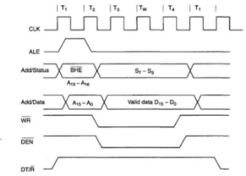
TIMING DIAGRAM of MINIMUM MODE 8086
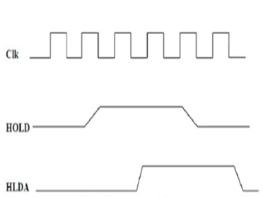
The HOLD pin is checked at the end of every bus cycle.
If active signal is received by the processor before T4 of the previous cycle, the CPU activates HLDA in the next clock cycle and the bus will be given to another requesting master.
|
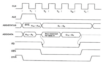
Fig 5 Cycle Timing Diagram For Minimum Operation
The control of the bus is not regained by the processor until the requesting master does not low HLDA pin.
|
Fig 6 Read Cycle Diagram for Minimum Mode
When the request drops by the requesting master, the HLDA is made low by the processor at the trailing edge of the next clock, as shown in Fig
|
Fig 7 Bus Request and Bus Grant Timing
TIMING DIAGRAM of MAXIMUM MODE 8086
|
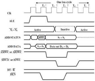
Fig 8: Memory Read Timing in Maximum Mode
|
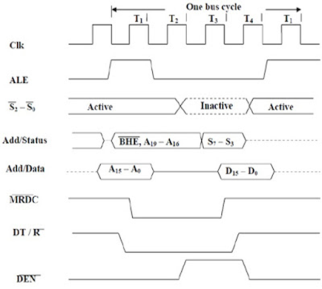
Fig 9 Memory Read Timing in Maximum Mode
Key takeaway
There are two operating modes
- Minimum mode
It can be selected by setting MN/MX pin to logic 1 and it acts like a single microprocessor.
- Maximum mode
This operation can be selected by setting MN/MX pin to logic 0 and microprocessor acts like a multiprocessor.
It provides the signals for implementing a multi core processor system environment and in this each processor executes its own program.
The 8086 microprocessor supports 8 different types of instructions. They are −
- Data Transfer Instructions
- Arithmetic Instructions
- Bit Manipulation Instructions
- String Instructions
- Program Execution Transfer Instructions (Branch & Loop Instructions)
- Processor Control Instructions
- Iteration Control Instructions
- Interrupt Instructions
Data Transfer Instructions
They are used for transferring the data from source operand to destination operand.
Instruction to transfer a word
- MOV – It is used to copy the byte from source to destination.
- PUSH − It is used to put a word at the top of the stack.
- POP − It gets a word from the top of the stack to the provided location.
- PUSHA − It puts all the registers into the stack.
- POPA − It gets words from the stack to all registers.
- XCHG − It exchanges the data from any two locations.
- XLAT − It translates a byte in AL using a table present in the memory.
Instructions for input and output port transfer
- IN − It reads a word from the given port to the accumulator.
- OUT − It sends out a word from the accumulator to the given port.
Instructions to transfer the address
- LEA − It loads the address of operand to the given register.
- LDS − Used to load DS register and other given register from the memory
- LES − Used to load ES register and other given register from the memory.
Instructions to transfer flag registers
- LAHF − It loads AH with the lower byte of the flag register.
- SAHF − It stores AH register to lower byte of the flag register.
- PUSHF − It copies the flag register at the top of the stack.
- POPF − It copies a word at the top of the stack.
They perform arithmetic operations like addition, subtraction, multiplication, division, etc.
Instructions to perform addition
- ADD − It adds the provided word to word.
- ADC − It adds word with carry.
- INC − It increments the provided byte by 1.
- AAA − It adjusts ASCII after addition.
- DAA − It is decimal adjust.
Instructions to perform subtraction
- SUB − It subtracts the byte from byte.
- SBB − It performs subtraction with borrow.
- DEC − It decrements the provided byte by 1.
- NPG − It negates each bit of the provided byte and add 1’s / 2’s complement.
- CMP − It compares two given byte/word.
- AAS − It adjusts ASCII codes after subtraction.
- DAS − It is decimal adjust after subtraction.
Instruction to perform multiplication
- MUL − It multiplies unsigned byte by byte or word by word.
- IMUL − It multiplies signed byte by byte or word by word.
- AAM − It adjusts ASCII codes after multiplication.
Instructions to perform division
- DIV − It divides the unsigned word or unsigned double word by word.
- IDIV − It divides the signed word or signed double word by word.
- AAD − It is ASCII adjust after division.
- CBW − It copies of sign bit of the lower byte.
- CWD − It fills the upper word of the double word with the sign bit of the lower word.
They perform operations that involves data bits i.e. operations like logical, shift, etc.
Instructions to perform logical operation
- NOT − It inverts each bit of a byte.
- AND − It adds each bit in a byte with the corresponding bit in another byte.
- OR − It multiplies each bit in a byte with the corresponding bit in another byte.
- XOR − It performs Exclusive-OR operation over each bit in a byte.
- TEST − It adds operands to update flags, without affecting operands.
Instructions to perform shift operations
- SHL/SAL − It shifts bits of a byte towards left by putting zero(S) in LSBs.
- SHR − It shifts bits of a byte towards right by putting zero(S) in MSBs.
- SAR − It shifts bits of a byte towards the right and copies the old MSB into the new MSB.
Instructions to perform rotate operations
- ROL − It rotates bits of word towards the left i.e. MSB to LSB.
- ROR − It rotates bits of word towards the right i.e. LSB to MSB.
- RCR − It rotates bits of word towards the right i.e. LSB to CF and CF to MSB.
- RCL − It rotates bits of word towards the left i.e. MSB to CF and CF to LSB.
It is a group of words and their memory is always placed in a sequential order.
Following are the instructions under this group −
- REP − It repeats the given instruction till CX ≠ 0.
- REPE/REPZ − It repeats the given instruction until zero flag ZF = 1 or CX = 0.
- REPNE/REPNZ − It repeats the given instruction until zero flag ZF = 1 or CX = 0.
- MOVS/MOVSB/MOVSW − It moves the byte from one string to another.
- COMS/COMPSB/COMPSW − It compares two string bytes.
- INS/INSB/INSW – It’s an input string byte from the I/O port given to the memory location.
- OUTS/OUTSB/OUTSW − It’s an input string byte from the memory location to the I/O port.
- SCAS/SCASB/SCASW − It scan’s a string and compares its byte with a byte present in AL or string word with a word present in AX.
- LODS/LODSB/LODSW − It stores the string byte into AL or AX.
Program Execution Transfer Instructions (Branch and Loop Instructions)
They are used to transfer/branch the instructions during an execution.
It includes −
Instructions to transfer the instruction during an execution without any condition −
- CALL − It calls a procedure and at the same time saves their return address to the stack.
- RET − It returns from the procedure to the main program.
- JMP − It jumps to the given address to proceed to the next instruction.
Instructions to transfer the instruction during an execution with some conditions −
- JA/JNBE − It jumps if instruction satisfies.
- JAE/JNB − It jumps if instruction satisfies.
- JBE/JNA − It jumps if instruction satisfies.
- JC − It jumps when carry flag is set.
- JE/JZ − It jumps when zero flag is set.
- JG/JNLE − It jumps when greater than / not less than / equal to instruction satisfies.
- JGE/JNL − It jumps when greater than / not less than / equal to instruction satisfies.
- JL/JNGE − It jumps when less than / not greater than / equal to instruction satisfies.
- JLE/JNG − − It jumps when less than / equal to / not greater than instruction satisfies.
- JNC − It jumps if no carry flag = 0
- JNE/JNZ − It jumps if no zero flag = 0
- JNO – Jump when overflow
- JNP/JPO – Jump when PF = 0
- JNS − Jump if no sign flag SF = 0
- JO – Jump when OF = 1
- JP/JPE – Jump when parity/ even parity PF = 1
- JS – Jump when SF = 1
Processor Control Instructions
These instructions are used to control the processor action by setting/resetting the flag values.
Following are the instructions under this group −
- STC – It sets CF to 1
- CLC – It clears CF to 0
- CMC − It complements the carry flag CF.
- STD − It sets the direction flag DF to 1
- CLD – It clears the direction flag DF to 0
- STI − It enables INTR input.
- CLI − It clears the interrupt enable flag.
Iteration Control Instructions
They are used to execute the given set of instructions for N number of times.
Following instructions are under this group −
- LOOP – It is a group of instructions that executes until the condition is satisfied i.e. CX = 0
- LOOPE/LOOPZ − It is a group of instructions that executes till it satisfies ZF = 1 & CX = 0
- LOOPNE/LOOPNZ − It is a group of instructions that executes till it satisfies ZF = 0 & CX = 0
- JCXZ − It jumps to the given address if CX = 0.
They are used to call the interrupt during program execution.
- INT − It interrupts the program execution and calling service specified.
- INTO − It interrupts the program execution if OF = 1
- IRET − It helps to return from interrupt service routine to the main program.
Key takeaway
The 8086 microprocessor supports 8 different types of instructions. They are −
- Data Transfer Instructions
- Arithmetic Instructions
- Bit Manipulation Instructions
- String Instructions
- Program Execution Transfer Instructions (Branch & Loop Instructions)
- Processor Control Instructions
- Iteration Control Instructions
- Interrupt Instructions
Discussed in section 3.3
- An interrupt is a condition that arises during the working of a microprocessor. The microprocessor services it by executing a subroutine called Interrupt Service Routine (ISR).
- There are three sources of interrupts for 8086:
Hardware interrupt-
These interrupts occur as signals on the external pins of the microprocessor. 8086 has two pins to accept hardware interrupts, NMI and INTR.
Software interrupt-
These interrupts occurs by writing the software interrupt instruction INT n where ‘n’ can be any value from 0 to 255 (00H to FFH). Hence all 256 interrupts can be invoked by software.
Error conditions (Exception or types)-
8086 is interrupted when some special conditions occur while executing certain instructions in the program. Example: An error in division automatically causes the INT 0 interrupt.
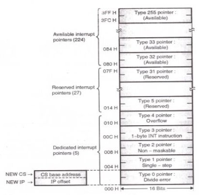
Interrupt Vector Table (IVT):
|
Fig 10 Interrupt Vector Table
- The interrupt vector (or interrupt pointer) table is the link between an interrupt type code and the procedure that has been designated to service interrupts associated with that code. 8086 supports total 256 types i.e. 00H to FFH.
- For each type of interrupt it has to reserve four bytes i.e. double word.
- The higher addressed word contains the base address of the segment and is normally referred as NEW CS.
- The lower addressed word consists of the procedure’s offset and is normally referred as NEW IP.
- Thus NEW CS provides new physical address from where user ISR routine will start.
- Here, four bytes (2 for NEW CS and 2 for NEW IP) are required; hence interrupt pointer table occupies up to the first 1k bytes (i.e. 256 x 4 = 1024 bytes) of lower order memory.
- The total interrupt vector table is divided into three groups namely,
Dedicated interrupts (INT 0…..INT 4)
Reserved interrupts (INT 5…..INT 31)
Available interrupts (INT 32…..INT 225)
- Dedicated interrupts (INT 0…..INT 4):
INT 0 (Divide Error)-
- This interrupt occurs whenever there is division error. This condition normally occurs when the divisor is very small as compared to the dividend or the divisor is zero.
- Its ISR address is stored at location 0 x 4 = 00000H in the IVT.
INT 1 (Single Step)-
- The microprocessor executes this interrupt after every instruction if the TF is set.
- Its ISR displays contents for all registers. Its ISR address is stored at location 1 x 4 = 00004H in the IVT.
INT 2 (Non mask-able Interrupt)-
- The microprocessor executes this ISR in response to an interrupt on the NMI (Non mask-able Interrupt) line.
- Its ISR address is stored at location 2 x 4 = 00008H in the IVT.
INT 3 (Breakpoint Interrupt)-
- This interrupt causes breakpoints in the program. It occurs by writing the instruction INT 03H or simply INT.
- It is useful in debugging large programs.
- Its ISR is used to display the contents of all registers on the screen. Its ISR address is stored at location 3 x 4 = 0000CH in the IVT.
INT 4 (Overflow Interrupt)-
- It occurs if the overflow flag is set and the microprocessor executes the INTO (Interrupt on Overflow) instruction.
- It detects overflow error in signed arithmetic operations.
- Its ISR address is stored at location 4 x 4 = 00010H in the IVT.
- Reserved interrupts (INT 5…..INT 31):
- These levels are reserved by Intel to be used in higher processors like 80386, Pentium etc. They are not available to the user.
- Available interrupts (INT 32…..INT 225):
- These are user defined, software interrupts.
- ISRs are written by the users to service various user defined conditions.
- These interrupts are invoked by writing the instruction INT n.
- Its ISR address is obtained by the microprocessor from location n x 4 in the IVT.
Hardware Interrupts:
NMI (Non mask-able interrupt)-
- This is a non-mask-able, edge triggered, high priority interrupt.
- On receiving this, the microprocessor executes INT instruction.
- Microprocessor obtains the ISR address from location 2 x 4 = 00008H from the IVT.
- It reads 4 locations starting from this address to get the values for IP and CS to execute the ISR.
INTR-
- This is a mask-able, level triggered, low priority interrupt.
- On receiving an interrupt on INTR line, the microprocessor executes 2 INTA pulses.
- It is masked by making IF = 0 by software through CLI instruction.
- It is unmasked by making IF = 1 by software through STI instruction.
Interrupt processing and pre-defined interrupts
The first five interrupt types are reserved for specific functions.

- INT 0 (Divide Error)-
- This interrupt occurs whenever there is division error. This condition normally occurs when the divisor is very small as compared to the dividend or the divisor is zero.
- Its ISR address is stored at location 0 x 4 = 00000H in the IVT.
- INT 1 (Single Step)-
- The microprocessor executes this interrupt after every instruction if the TF is set.
- Its ISR displays contents for all registers. Its ISR address is stored at location 1 x 4 = 00004H in the IVT.
- INT 2 (Non mask-able Interrupt)-
- The microprocessor executes this ISR in response to an interrupt on the NMI (Non mask-able Interrupt) line.
- Its ISR address is stored at location 2 x 4 = 00008H in the IVT.
- INT 3 (Breakpoint Interrupt)-
- This interrupt causes breakpoints in the program. It occurs by writing the instruction INT 03H or simply INT.
- It is useful in debugging large programs.
- Its ISR is used to display the contents of all registers on the screen. Its ISR address is stored at location 3 x 4 = 0000CH in the IVT.
- INT 4 (Overflow Interrupt)-
- It occurs if the overflow flag is set and the microprocessor executes the INTO (Interrupt on Overflow) instruction.
- It detects overflow error in signed arithmetic operations.
- Its ISR address is stored at location 4 x 4 = 00010H in the IVT.
Key takeaway
An interrupt is a condition that arises during the working of a microprocessor. The microprocessor services it by executing a subroutine called Interrupt Service Routine (ISR).
The total interrupt vector table is divided into three groups namely,
Dedicated interrupts (INT 0…..INT 4)
Reserved interrupts (INT 5…..INT 31)
Available interrupts (INT 32…..INT 225)
Reference:
1. Gaonkar, Ramesh S , “Microprocessor Architecture, Programming and Applications with 8085”, Penram International Publishing.
2. Ray A K, Bhurchandi K M, “Advanced Microprocessors and Peripherals”, TMH Hall D V, Microprocessor Interfacing’, TMH
3.Liu and, “Introduction to Microprocessor”, TMH
4. Brey, Barry B, “INTEL Microprocessors”, PHI

