Unit – 2
MSI devices like comparators
A comparator is a logic circuit, used to compare the magnitude of two binary numbers.
The following figure shows the block diagram of a n-bit comparator.
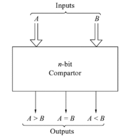
Fig.: Comparator
It receives two n-bit numbers A and B as inputs and the outputs are A>B, A=B and A<B. Depending upon the relative magnitude of the two numbers, one of the outputs will be high.
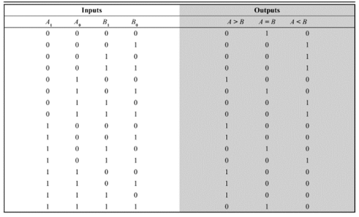
The following is the truth table of a 2-bit comparator.
- It is a special type of combinational circuit.
- It has n-data inputs, one output and m inputs select lines with 2m = n.
- It selects one of the n data inputs and routes it to the output.
- The selection of one of the inputs is done by the select lines.
- Depending on the code applied at the inputs, one of the n data sources is selected and transmitted to the single output Y.
- E is the enable input which is useful for cascading purpose.
- It is an active low terminal hence performs the required operation when it is low.
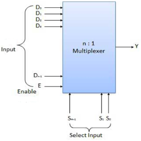
Fig.: Block diagram of multiplexer
Multiplexers come in multiple variations
- 2: 1 multiplexer
- 4: 1 multiplexer
- 16: 1 multiplexer
- 32: 1 multiplexer
Block Diagram of 2:1 MUX
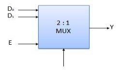
Fig.: 2:1 MUX
Truth Table of 2:1 MUX
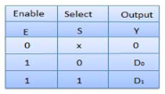
Where x is don’t care.
Key Takeaways
- It has n-data inputs, one output and m inputs select lines with 2m = n.
- The selection of one of the inputs is done by the select lines.
- Binary code of N digits is used to store 2N distinct elements of coded information.
- This is the reason why encoders and decoders are used.
- Encoders convert 2N lines of input into a code of N bits and Decoders decode those N bits into 2N lines.
- Encoders –
- It is a combinational circuit that converts binary information in the form of a 2N input lines into N output lines, which represent N bit code for the input.
- For simple encoders, only one input line is active at a time.
- For example: Octal to Binary encoder takes 8 input lines and generates 3 output lines.
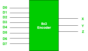
Fig.: 8X3 Encoder (ref. 2)
Truth Table –
D7 | D6 | D5 | D4 | D3 | D2 | D1 | D0 | X | Y | Z |
0 | 0 | 0 | 0 | 0 | 0 | 0 | 1 | 0 | 0 | 0 |
0 | 0 | 0 | 0 | 0 | 0 | 1 | 0 | 0 | 0 | 1 |
0 | 0 | 0 | 0 | 0 | 1 | 0 | 0 | 0 | 1 | 0 |
0 | 0 | 0 | 0 | 1 | 0 | 0 | 0 | 0 | 1 | 1 |
0 | 0 | 0 | 1 | 0 | 0 | 0 | 0 | 1 | 0 | 0 |
0 | 0 | 1 | 0 | 0 | 0 | 0 | 0 | 1 | 0 | 1 |
0 | 1 | 0 | 0 | 0 | 0 | 0 | 0 | 1 | 1 | 0 |
1 | 0 | 0 | 0 | 0 | 0 | 0 | 0 | 1 | 1 | 1 |
- From the above truth table, it is seen that the output is 000 when D0 is active; 001 when D1 is active; 010 when D2 is active and so on.
Implementation –
- From the above truth table, the output Z is active when the input octal digit is 1, 3, 5 or 7.
- Y is active when input octal digit is 2, 3, 6 or 7 and X is active when input octal digits 4, 5, 6 or 7.
- Hence, the Boolean functions would be:
X = D4 + D5 + D6 + D7
Y = D2 +D3 + D6 + D7
Z = D1 + D3 + D5 + D7
- Hence, the encoder is realized with OR gates as follows:
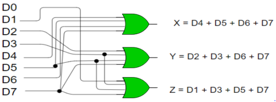
Fig: 8:3 encoder (ref.2)
- Limitation of the encoder is that only one input is active at a time.
- If more than one input is active, then the output of encoder is undefined.
- For example, if D6 and D3 are both active, then, our output would be 111 which is the output for D7.
- Problem arises when all inputs are 0.
- The encoder gives output 000 which actually is the output for D0. To avoid this, an extra bit is added to the output which is called the valid bit whose value is 0 when all inputs are 0 or 1.
Priority Encoder:
- It is an encoder whose inputs are given priorities.
- When more than one input becomes active at the same time then the input with higher priority takes precedence w.r.to the output which is generated.
- Considering a 4:2 priority encoder.
- From the truth table given below we see that when all inputs are 0, V bit is zero and outputs are not used.
- The x in the table shows the don’t care condition, i.e. it can be 0 or 1.
- Here, D3 has highest priority, therefore, when D3 is high, output has to be 11.
- D0 has the lowest priority, hence the output would be 00 only when D0 is high and all the other input lines are low.
Truth Table –
D3 | D2 | D1 | D0 | X | Y | V |
0 | 0 | 0 | 0 | x | x | 0 |
0 | 0 | 0 | 1 | 0 | 0 | 1 |
0 | 0 | 1 | x | 0 | 1 | 1 |
0 | 1 | X | x | 1 | 0 | 1 |
1 | x | X | x | 1 | 1 | 1 |
Implementation –
The condition for valid bit to be 1 is when at least one of the inputs should be high. Hence,
V = D0 + D1 + D2 + D3
For X:
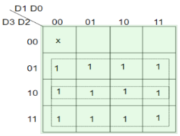
=>X=D2+D3
For Y:
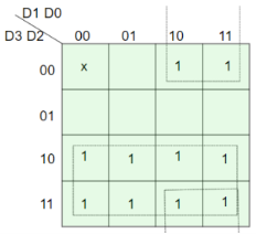
=> Y = D1 D2’ + D3
Hence, the priority 4-to-2 encoder can be realized as follows:
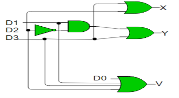
Fig: Priority encoder (ref.2)
Key takeaway
An Encoder is a combinational circuit that performs the reverse operation of Decoder. It has maximum of 2n input lines and ‘n’ output lines. It will produce a binary code equivalent to the input, which is active High.
- It works as an inverse of an encoder.
- It is a combinational circuit which converts n input lines into 2n output lines.
- Taking an example of 3-to-8-line decoder.
Truth Table –
X | Y | Z | D0 | D1 | D2 | D3 | D4 | D5 | D6 | D7 |
0 | 0 | 0 | 1 | 0 | 0 | 0 | 0 | 0 | 0 | 0 |
0 | 0 | 1 | 0 | 1 | 0 | 0 | 0 | 0 | 0 | 0 |
0 | 1 | 0 | 0 | 0 | 1 | 0 | 0 | 0 | 0 | 0 |
0 | 1 | 1 | 0 | 0 | 0 | 1 | 0 | 0 | 0 | 0 |
1 | 0 | 0 | 0 | 0 | 0 | 0 | 1 | 0 | 0 | 0 |
1 | 0 | 1 | 0 | 0 | 0 | 0 | 0 | 1 | 0 | 0 |
1 | 1 | 0 | 0 | 0 | 0 | 0 | 0 | 0 | 1 | 0 |
1 | 1 | 1 | 0 | 0 | 0 | 0 | 0 | 0 | 0 | 1 |
Implementation
D0 is high when X = 0, Y = 0 and Z = 0. Hence,
D0 = X’ Y’ Z’
Similarly,
D1 = X’ Y’ Z
D2 = X’ Y Z’
D3 = X’ Y Z
D4 = X Y’ Z’
D5 = X Y’ Z
D6 = X Y Z’
D7 = X Y Z
Hence,
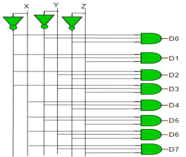
Fig: Decoder (ref.2)
Key Takeaways:
- It works as an inverse of an encoder.
- It is a combinational circuit which converts n input lines into 2n output lines.
Multiplexed displays are basically multiple displays which are multiplexed together and usually one is turned on at a time, the turning on and off of multiple displays are so fast that viewer is able to believe that all the displays are turned on at a time.
Multiplexing of displays have some benefits like reduced number of input pins, reduced complexity and less power is required for the display. In this article we will use 4-digit 7 segment multiplexed display and understand how to drive the display using Arduino.
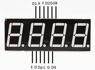
Fig: 4-digit 7 segment display
In above picture we can see total 12 pins. 4 pins for turning on individual digit and 8 pins for segment A-G and DP. Let's look into diagram below how the led's are multiplexed inside this display.
 Fig: 4-digit 7 segment display multiplexed
In Fig 2 we have a common anode display since all the positives of segments (A-G and DP) are connected to a single pin. Also, we have segment pins of a digit are connected with segment pins of other digits, so we have common pins for segments across digits and this is called a multiplexed display. We have 4 columns for each individual digit and 8 rows for 7 segments and for a decimal point. Whenever we want to display a number can be driven from 8 rows and on whichever digit it has to be displayed can be driven by 4 columns.
Now problem is if we want to display 1111 it is easy as we can give output high to D1, D2, D3, D4 (4 columns to turn on all 4 digits) and low to b, c (segment b and c is to drive number 1 on a seven segment). But in case if want to display 1234 we cannot do it simply, if we drive 1 using segments then all the digits will display 1 since there is no separate segment pins for each individual digit.
Half Adder
- It is a combinational circuit which has two inputs and two outputs.
- It is designed to add two single bit binary number A and B.
- It has two outputs carry and sum.
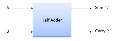
Fig.: Half adder
Truth Table
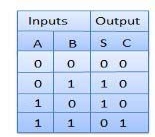
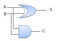
Fig.: Half adder Circuit Diagram
Full Adder
- It is developed to overcome the drawback of Half Adder circuit.
- It can add two one-bit numbers A and B and a carry C.
- It is a three input and two output combinational circuit.
Block diagram
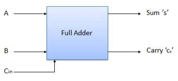
Fig.: Full adder
Truth Table
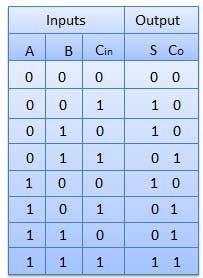
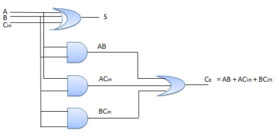
Fig.: Full adder Circuit Diagram
Key Takeaways:
- Half adder is a combinational circuit which has two inputs and two outputs.
- Since there is no provision for carry in half adder, full adder is developed to overcome the drawback.
Subtractor
Half Subtractors
- It is a combination circuit with two inputs and two outputs.
- The difference between the two binary bits is obtained at the output and an output (Borrow) indicates if a 1 has been borrowed.
- Here A is called as Minuend bit and B is called as Subtrahend bit.
Truth Table
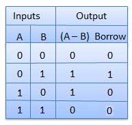
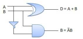
Fig.: Half subtractor Circuit Diagram
Full Subtractors
It is a combinational circuit which has three inputs A, B, C and two output D and C'.
A is the 'minuend', B is 'subtrahend', C is the 'borrow' which is produced by the previous stage, difference output D and C' is the borrow output.
Truth Table
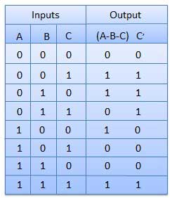
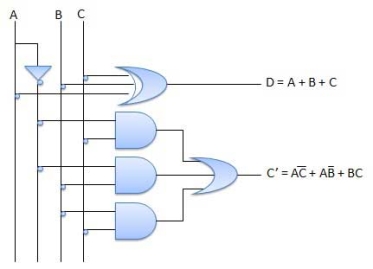
Fig.: Full subtractor Circuit Diagram
Key Takeaways:
- Half subtractor is a combinational circuit which has two inputs and two outputs.
- Since there is no provision for borrow in half subtractor, full subtractor is developed to overcome the drawback.
Serial adder
Serial binary adder is a combinational logic circuit that performs the addition of two binary numbers in serial form. Serial binary adder performs bit by bit addition. Two shift registers are used to store the binary numbers that are to be added.
A single full adder is used to add one pair of bits at a time along with the carry. The carry output from the full adder is applied to a D flip-flop. After that output is used as carry for next significant bits. The sum bit from the output of the full adder can be transferred into a third shift register.
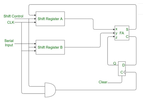
Fig: Block diagram of Serial Binary Adder
Parallel adders
A parallel adder is a combinational digital circuit that adds two binary numbers in parallel form. It consists of full adders connected in cascade, with the output carry from each full adder connected to the input carry of the next full adder.
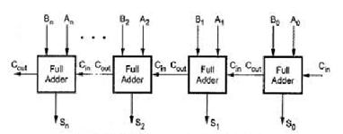
Fig.: Parallel Adder
BCD stands for binary coded decimal.
Suppose, we have two 4-bit numbers A and B. The value of A and B can vary from 0(0000 in binary) to 9(1001 in binary).
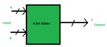
Fig.: BCD adder (ref. 2)
- The output varies from 0 to 18 if the carry from the previous sum is not considered.
- But if we consider the carry, then the maximum value of output will be 19 (i.e., 9+9+1 = 19).
- When we simply add A and B, then we get the binary sum, and to get the output in BCD form, we use BCD Adder.
Example 1:
Input:
A = 0111 B = 1000
Output:
Y = 1 0101
Explanation: We are adding A (=7) and B (=8).
The value of the binary sum will be 1111(=15).
But the BCD sum will be 1 0101,
Where 1 is 0001 in binary and 5 is 0101 in binary.
Example 2:
Input:
A = 0101 B = 1001
Output:
Y = 1 0100
Explanation: We are adding A (=5) and B (=9).
The value of the binary sum will be 1110(=14).
But the BCD sum will be 1 0100,
Where 1 is 0001 in binary and 4 is 0100 in binary.
Now, let's move to the table and find out the logic when we are going to add “0110”.
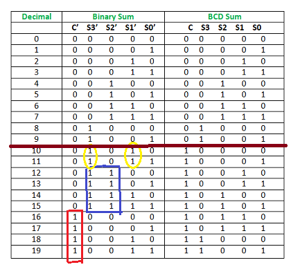
Fig.: Table explaining BCD addition (ref. 2)
We are adding “0110” (=6) only to the second half of the table because of the following conditions:
- If C’ = 1 (Satisfies 16-19)
- If S3′. S2′ = 1 (Satisfies 12-15)
- If S3′. S1′ = 1 (Satisfies 10 and 11)
So, our logic is
C' + S3’. S2' + S3’. S1' = 1
Implementation:
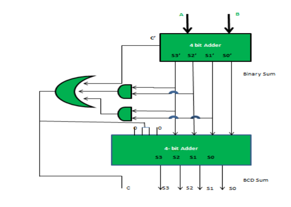
Fig.18: BCD adder (ref. 2)
Barrel shifter
A barrel shifter is a digital circuit used to rotate the data fed to it by a specified number bits. The specialty of this circuit is that it is able to achieve this rotation without the use of flipflops (sequential circuits), instead it uses logic gates to give the rotated value instantaneously (assuming zero gate delay).
At the block level it can be seen as:
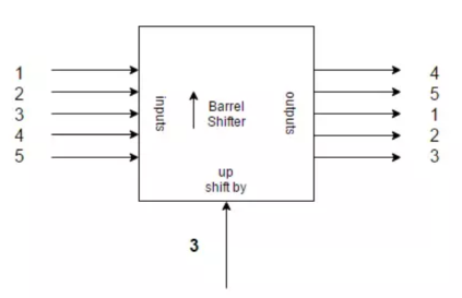
Fig: Barrel Shifter
The above block diagram shows an example of a 5-bit barrel shifter which up shifts the bits by the specified number. The up-shift value fed to the barrel shifter in the above figure is 3.
Hence the output shows the inputs up shifted in circular fashion by 3.
These circuits generally have complex use cases in Computer Architecture like, Rotate operation in ALU, floating point operations, arbitration of resource etc.
ALU
ALU is the most widely used combinational circuit that is capable of performing arithmetic as well as logical operations. The following figure gives the block diagram of ALU:
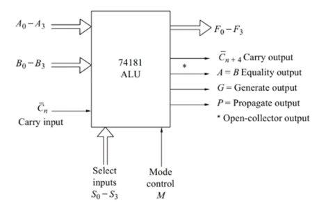
The functions of various input, output and control lines are given below:
A and B: 4- bit binary data input
 n: Carry input (active low)
F: 4-bit binary data output
 n+4: Carry output (active low) – For subtraction operation, it indicates the sign of the output. Logic 0 indicates positive result and logic 1 indicates negative result expressed in 2’s complement form.
A=B: Logic 1 on this line indicates A=B
G: Carry generate output
P: Carry Propagate output
Select input(S): Used to select any operation (refer table below)
Mode control(M): M=0 Arithmetic operations
M=1 Logic Operations
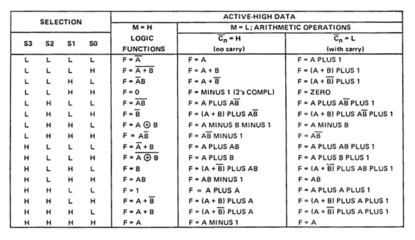
Following is the function table of the 74181 ALU:
Example: Design an 8-bit adder/subtractor using 74181s in cascade. Show how it works for A=97 and B=29
Solution: The least significant 4-bits of A and B are applied at the A and B inputs of the least significant 74181 and the most significant 4-bits of A and B are applied at the A and B inputs of the most significant 74181. The carry out of the least significant 74181 is connected to the carry-in of the most significant 74181. The 8-bit output will be available on F outputs. The select lines of both the 74181s are connected together.
Addition is performed with M=0 and =1001, and subtraction is performed with M=0 and S=0110. Connect  n of least significant 74181 to 1 for addition and 0 for subtraction.
Therefore, for A= 97 (01100001) and B=29(00011101)

References:
1. John Yarbrough, ―Digital Logic Applications and Design, Cengage Learning, ISBN – 13: 978-81-315-0058-3
2. D. Leach, Malvino, Saha, ―Digital Principles and Applications‖, Tata McGraw Hill, ISBN – 13:978-0-07-014170-4.
3. Anil Maini, ―Digital Electronics: Principles and Integrated Circuits‖, Wiley India Ltd, ISBN:978-81-265-1466-3.
4. Norman B & Bradley, ―Digital Logic Design Principles, Wiley India Ltd, ISBN:978-81-265-1258