Unit – 3
Sequential logic design
S-R Flip Flop:
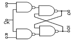
S | R |  |  |
0 | 0 | 0 | 0 |
0 | 0 | 1 | 1 |
0 | 1 | 0 | 0 |
0 | 1 | 1 | 0 |
1 | 0 | 0 | 1 |
1 | 0 | 1 | 1 |
1 | 1 | 0 | - |
1 | 1 | 1 | - |
J-K Flip Flop:
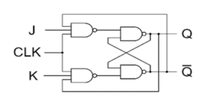
S | R |  |  |
0 | 0 | 0 | 0 |
0 | 0 | 1 | 1 |
0 | 1 | 0 | 0 |
0 | 1 | 1 | 0 |
1 | 0 | 0 | 1 |
1 | 0 | 1 | 1 |
1 | 1 | 0 | 1 |
1 | 1 | 1 | 0 |
Race Around Condition in JK Flip-flop –
- For J-K flip-flop, if J=K=1, and if clk=1 for a long period of time, then output Q will toggle as long as CLK remains high which makes the output unstable or uncertain.
- This problem is known as race around condition in J-K flip-flop.
- This problem can be avoided by ensuring that the clock input is at logic “1” only for a very short time.
- Hence the concept of Master Slave JK flip flop was introduced.
Master Slave JK flip flop –
It is basically a combination of two JK flip-flops connected together in series.
The first is the “master” and the other is a “slave”.
The output from the master is connected to the two inputs of the slave whose output is fed back to inputs of the master.
In addition to these two flip-flops, the circuit comprises of an inverter.
The inverter is connected to clock pulse in such a way that an inverted clock pulse is given to the slave flip-flop.
In other words, if CP=0 for a master flip-flop, then CP=1 for a slave flip-flop and vice versa.
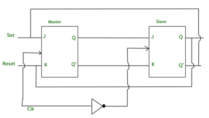
Fig. Master Slave Flip flop
Working of a master slave flip flop –
- When the clock pulse goes high, the slave is isolated; J and K inputs can affect the state of the system. The slave flip-flop is isolated when the CP goes low. When the CP goes back to 0, information is transmitted from the master flip-flop to the slave flip-flop and output is obtained.
- The master flip flop is positive level triggered and the slave flip flop is negative level triggered, hence the master responds prior to the slave.
- If J=0 and K=1, Q’ = 1 then the master goes to the K input of the slave and the clock forces the slave to reset therefore the slave copies the master.
- If J=1 and K=0, Q = 1 then the master goes to the J input of the slave and the Negative transition of the clock sets the slave and thus copy the master.
- If J=1 and K=1, the master toggles on the positive transition and the slave toggles on the negative transition of the clock.
- If J=0 and K=0, the flip flop becomes disabled and Q remains unchanged.
Timing Diagram of a Master flip flop –
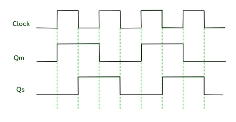
- When the CP = 1 then the output of master is high and remains high till CP = 0 because the state is stored.
- Now the output of master becomes low when the clock CP = 1 and remains low until the clock becomes high again.
- Thus, toggling takes place for a clock cycle.
- When the CP = 1 then the master is operational but not the slave.
- When the clock is low, the slave becomes operational and remains high until the clock again becomes low.
- Toggling takes place during the whole process since the output changes once in a cycle.
- This makes the Master-Slave J-K flip flop a Synchronous device which passes data with the clock signal.
D Flip Flop:
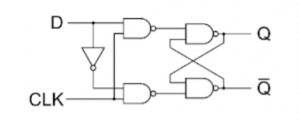
Q | D | Q(t+1) |
0 | 0 | 0 |
0 | 1 | 1 |
1 | 0 | 0 |
1 | 1 | 1 |
T Flip Flop:
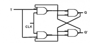
T |  |  |
0 0 1 1 | 0 1 0 1 | 0 1 1 0 |
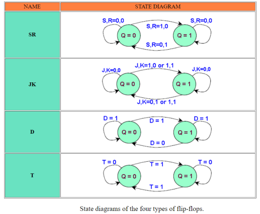
In addition to graphical symbols, tables or equations, flip-flops can also be represented graphically by a state diagram. In this diagram, a state is represented by a circle, and the transition between states is indicated by directed lines (or arcs) connecting the circles.
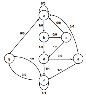
The reduction of the number of flip-flops in a sequential circuit is referred to as the state reduction problem. State-reduction algorithms are concerned with procedures for reducing the number of states in a state table, while keeping the external input-output requirements unchanged. Since (N) flip-flops produce (2N) states, a reduction in the number of states may (or may not) result in a reduction in the number of flip-flops. An unpredictable effect in reducing the number of flip-flops is that sometimes the equivalent circuit (with fewer flip-flops) may require more combinational gates. We will illustrate the state reduction procedure with an example. We start with a sequential circuit whose specification is given in the state diagram shown in Fig. (1). In this example, only the input-output sequences are important; the internal states are used merely to provide the required sequences. For this reason, the states marked inside the circles are denoted by letter symbols instead of their binary values. This is in constant to a binary counter, where the binary value sequence of the state themselves is taken as the outputs.
An algorithm for the state reduction quotes that:
“Two states are said to be equivalent if, for each member of the set of inputs, they give exactly the same output and send the circuit either to the same state or to an equivalent state.”
Now apply this algorithm to the state table of the circuit:
Present State | Next State | Output | ||
 |  |  |  | |
a b c d e f g | a c a e a g a | b d d f f f f | 0 0 0 0 0 0 0 | 0 0 0 1 1 1 1 |
States g and e both go to states a and f and have outputs of 0 and 1 for x = 0 and x = 1, respectively.
The procedure for removing a state and replacing it by its equivalent is demonstrated in the following table:
Present State | Next State | Output | ||
 |  |  |  | |
a b c d e f | a c a e a e | b d d f f f | 0 0 0 0 0 0 | 0 0 0 1 1 1 |
Thus, the row with present state g is removed and stage g is replaced by state e each time it occurs in the next state columns. Present state f now has next states e and f and outputs 0 and 1 for x = 0 and x = 1. The same next states and outputs appear in the row with present state d. Therefore, states f and d are equivalent and can be removed and replaced with d.
The final reduced state table is:
Present State | Next State | Output | ||
 |  |  |  | |
a b c d e | a c a e a | b d d d d | 0 0 0 0 0 | 0 0 0 1 1 |
The state diagram for the above reduced table is:
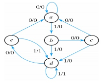
This state diagram satisfies the original input output specifications.
Applying the input sequence previously used, the following list is obtained:
State | a | a | b | c | d | e | d | d | e | d | e | a |
Input | 0 | 1 | 0 | 1 | 0 | 1 | 1 | 0 | 1 | 0 | 0 |
|
Output | 0 | 0 | 0 | 0 | 0 | 1 | 1 | 0 | 1 | 0 | 0 |
|
Note that the same output sequence results, although the state sequence is different.
Ripple (Asynchronous) Counters
- In this universal clock is not used and only the first flip flop is driven by main clock and the clock input of rest of the following is driven by output of previous flip flops.

Asynchronous counter
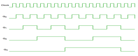
Timing diagram of Asynchronous counter
- It is seen from timing diagram that Q0 is changing as soon as the rising edge of clock pulse is encountered.
- Q1 is changing when rising edge of Q0 is encountered and so on.
- In this way ripples are generated through Q0, Q1, Q2, Q3 and therefore it is also called as a RIPPLE counter.
Synchronous Counters
- It has one global clock which drives each and every flip flop and hence output changes in parallel.
- The advantage of synchronous counter over asynchronous counter is that it can operate on higher frequency and it does not have cumulative delay.
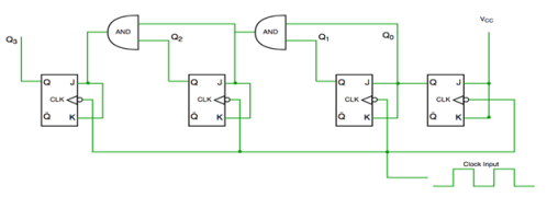
Synchronous counter
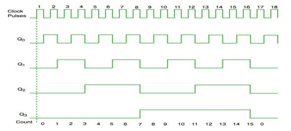
Timing diagram of synchronous counter
- Flip flops are used to store one bit of binary data (1or 0).
- If we need to store multiple bits of data, we use multiple flip flops.
- N flip flops are connected to store n bits of data.
- A Register is a device which stores such information. It is a group of flip flops connected in series which is used to store multiple bits of data.
- The information stored in these registers can be transferred with the help of shift registers.
- This register is a group of flip flops used to store multiple bits of data.
- The bits stored in these registers can be moved in/out of the registers by applying clock pulses.
- The registers which shift the bits towards left are called “Shift left registers”.
The registers which shift the bits towards right are called “Shift right registers”.
Shift registers are of 4 types and they are:
- Serial In Serial Out register
- Serial In parallel Out register
- Parallel In Serial Out register
- Parallel In parallel Out register
Serial-In Serial-Out Shift Register (SISO) –
- It allows serial input i.e., one bit after another and produces a serial output is known as Serial-In Serial-Out shift register.
- Since it has one output, the data leaves the register one bit at a time in a serial pattern, hence known as Serial-In Serial-Out Shift Register.
- The logic circuit is given underneath.
- The circuit comprises four D flip-flops which are connected serially.
- All these flip-flops are synchronous.

Fig. SISO
Serial-In Parallel-Out shift Register (SIPO) –
- It allows serial input through a single data line and produces a parallel output.
- The logic circuit is given underneath.
- The circuit consists of four D flip-flops which are connected synchronously.
- The clear (CLR) signal is also connected to all the 4 flip flops to RESET them.
- The output of the first flip flop is sent to the input of the next and so on.
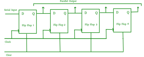
Fig. SIPO
- They are used in communication lines because the main use of the SIPO register is to convert serial data into parallel data.
Parallel-In Serial-Out Shift Register (PISO) –
- It allows parallel input data and produces a serial output.
- The logic circuit is given underneath.
- The circuit comprises four D flip-flops which are connected synchronously.
- The clock is connected to all the flip flops but the input data is connected to each flip flop individually through a multiplexer.
- The output of the previous flip flop and parallel data input are connected to the input of the MUX and the output of MUX is connected to the next flip flop.
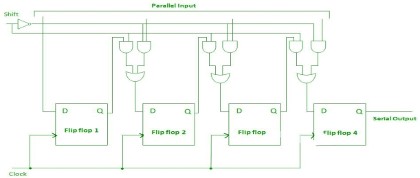
Fig. PISO
- It used to convert parallel data to serial data.
Parallel-In Parallel-Out Shift Register (PIPO) –
- It allows parallel input data and produces a parallel output.
- The logic circuit is given underneath.
- The circuit comprises four D flip-flops which are connected synchronously.
- The clear (CLR) and clock signals are connected to all flip flops.
- In this, there are no interconnections between flip-flops as no serial shifting of the data is required.
- Data is provided separately as input for each flip flop and the output is also collected individually from each flip flop.
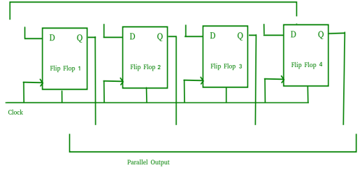
Fig. PIPO
- It is used as a temporary storage device and it acts as a delay element too.
Bidirectional Shift Register –
- If a binary number is shifted towards left by one position, then it is equivalent to multiplying the number by 2 and if a binary number towards the right by one position, then it is equal to dividing the number by 2.
- To perform the above operations a register is used which can shift the data in either direction.
- Hence, Bidirectional shift registers are capable of shifting the data either right or left depending on the mode selected.
- If the mode =1(high), then the data is shifted towards the right, and if the mode = 0(low), then the data is shifted towards the left direction.
- The logic circuit is given underneath.
- The circuit comprises four D flip-flops which are connected synchronously.
- The input data is connected at two ends of the circuit and depending on the model and gate selected.
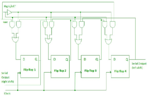
Fig. Bidirectional shift register
Applications Of Shift Registers
- They are used for temporary data storage.
- They are used for data transfer and data manipulation.
- The SISO and PIPO registers are used to produce time delay in digital circuits.
- The SIPO register is used for conversion of serial data to parallel data hence they are used in communication lines.
- A PISO register is used to convert parallel data to serial data.
A synchronous sequential circuit is also called as Finite State Machine FSM, if it has finite number of states. There are two types of FSMs.
- Mealy State Machine
- Moore State Machine
Mealy Machine vs. Moore Machine
The following table highlights the points that differentiate a Mealy Machine from a Moore Machine.
Mealy Machine | Moore Machine |
Output depends both upon the present state and the present input | Output depends only upon the present state. |
Generally, it has fewer states than Moore Machine. | Generally, it has more states than Mealy Machine. |
The value of the output function is a function of the transitions and the changes, when the input logic on the present state is done. | The value of the output function is a function of the current state and the changes at the clock edges, whenever state changes occur. |
Mealy machines react faster to inputs. They generally react in the same clock cycle. | In Moore machines, more logic is required to decode the outputs resulting in more circuit delays. They generally react one clock cycle later. |
Mealy Machine
A Mealy Machine is an FSM whose output depends on the present state as well as the present input.
It can be described by a 6 tuple (Q, ∑, O, δ, X, q0) where −
- Q is a finite set of states.
- ∑ is a finite set of symbols called the input alphabet.
- O is a finite set of symbols called the output alphabet.
- δ is the input transition function where δ: Q × ∑ → Q
- X is the output transition function where X: Q × ∑ → O
- q0 is the initial state from where any input is processed (q0 ∈ Q).
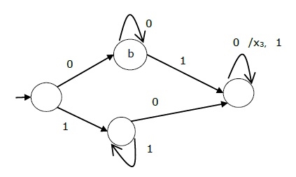
The state table of a Mealy Machine is shown below −
Present state | Next state | |||
Input = 0 | Input = 1 | |||
State | Output | State | Output | |
→ a | b | x1 | c | x1 |
b | b | x2 | d | x3 |
c | d | x3 | c | x1 |
d | d | x3 | d | x2 |
The state diagram of the above Mealy Machine is −
Moore Machine
Moore machine is an FSM whose outputs depend on only the present state.
A Moore machine can be described by a 6 tuple (Q, ∑, O, δ, X, q0) where −
- Q is a finite set of states.
- ∑ is a finite set of symbols called the input alphabet.
- O is a finite set of symbols called the output alphabet.
- δ is the input transition function where δ: Q × ∑ → Q
- X is the output transition function where X: Q → O
- q0 is the initial state from where any input is processed (q0 ∈ Q).
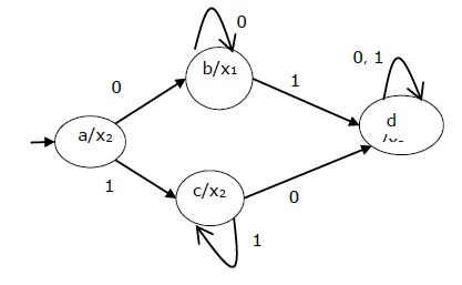
The state table of a Moore Machine is shown below −
Present state | Next State | Output | |
Input = 0 | Input = 1 | ||
→ a | b | c | x2 |
b | b | d | x1 |
c | c | d | x2 |
d | d | d | x3 |
The state diagram of the above Moore Machine is −
ASM stands for 'Algorithm State Machine 'or simply state machine is another name given to sequential network is used to control a digital system which carries out a step by a step –by step procedure. It should be noted that ASM charts represent physical hardware and offers several advantages.
1. Operation of a digital system can be easily understood by inspection of the SM chart.
2. ASM charts represent physical hardware.
3. The ASM chart are equivalent to a state graph, and it leads directly to a hardware realization.
4. ASM charts can be described the operation of both combinational and sequential circuits.
5. ASM charts are easier to understand and can be converted several equivalent forms.
6. The ASM chart may be equivalently expressed as a state and output table.
Following are the three basic components of ASM charts.
- State box
- Decision box
- Conditional output box
State box
State box is represented in rectangular shape. Each state box represents one state of the sequential circuit. The symbol of state box is shown in the following figure.
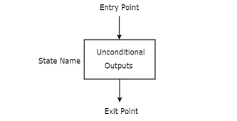
It is having one entry point and one exit point. Name of the state is placed to the left of state box. The unconditional outputs corresponding to that state can be placed inside state box. Moore state machine outputs can also be placed inside state box.
Decision box
Decision box is represented in diamond shape. The symbol of decision box is shown in the following figure.
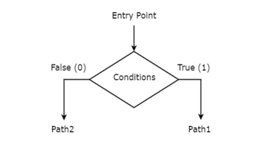
It is having one entry point and two exit paths. The inputs or Boolean expressions can be placed inside the decision box, which are to be checked whether they are true or false. If the condition is true, then it will prefer path1. Otherwise, it will prefer path2.
Conditional output box
Conditional output box is represented in oval shape. The symbol of conditional output box is shown in the following figure.
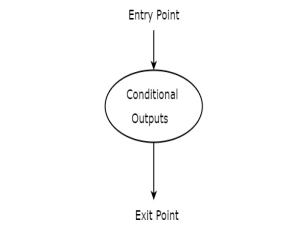
It is also having one entry point and one exit point similar to state box. The conditional outputs can be placed inside state box. In general, Mealy state machine outputs are represented inside conditional output box. So, based on the requirement, we can use the above components properly for drawing ASM charts.
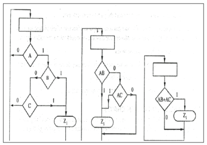
Example 1
Convert the state diagram of Fig. Below to ASM chart.
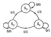
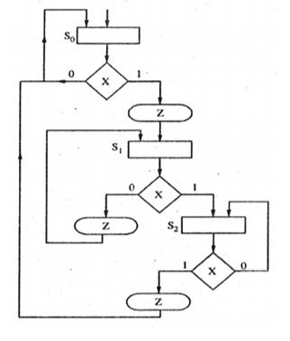
Sol:
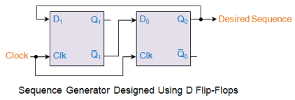
The sequence generators are nothing but a set of digital circuits which are designed to result in a specific bit sequence at their output. There are several ways in which these circuits can be designed including those which are based on multiplexers and flip-flops.
As an example, let us consider that we intend to design a circuit which moves through the states 0-1-3-2 before repeating the same pattern. The steps involved during this process are as follows.
- At first, we need to determine the number of flip-flops which would be required to achieve our objective. In our example, there are 4 states which are identical to the states of a 2-bit counter except the order in which they transit. From this, we can guess the requirement of flip-flops to be 2 in order to achieve our objective.
- The state transition table is shown by the first four columns of Table I in which the first two columns indicate the present states while the next two columns indicate the corresponding next states. For instance, first state in our example is 0 = “00” which leads to the next state 1 = “01”.
- Now this state transition table is to be extended so as to include the excitation table of the flip-flop with which we desire to design our circuit. In our case, it is nothing but D flip-flop due to which we have the fifth and the sixth columns of the table representing the excitation table of D flip-flop.
For example, look at the orange shaded row in Table I in which the present and the next states 1 and 0 (respectively) result in D1 to be 0. The same row also shows the case wherein

Present States | Next States | Inputs of D flip-flops | |||
Q1 | Q0 | Q1+ | Q0+ | D1 | D0 |
0 | 0 | 0 | 1 | 0 | 1 |
0 | 1 | 1 | 1 | 1 | 1 |
1 | 1 | 1 | 0 | 1 | 0 |
1 | 0 | 0 | 0 | 0 | 0 |
Now it’s time to derive the Boolean expressions for D1 and D0. This can be done using any kind of simplification technique including K-map. However, as our example is quite simple, we can just use the Boolean laws to solve for D1 and D0. Thus


Having known the inputs to either of the D flip-flops, now we can design our sequence generator as shown in this figure.
References:
1. Anand Kumar, “Fundamentals of Digital Circuits”, Prentice Hall of India, 1st Edition.
2. J. F. Wakerly, “Digital Design- Principles and Practices,”, Pearson, 3rd Edition.
3. M. M. Mano, “Digital Design,” Prentice Hall India.