Unit – 4
Logic families and semiconductor memories
The circuit diagram of a 2 input TTL NAND gate is as follows:
- A two input TTL NAND is shown above. A and B are two inputs while Y is the output.
- Operation of the gate:
a) A and B both low: both B-E junctions of Q1 are forward biased. Hence D1 and D2 will conduct to force the voltage at point C to 0.7V. This voltage is insufficient to forward bias B-E junction of Q2. Hence Q2 remains OFF. Therefore, its collector voltage rises to VCCVCC. As Q3 is operating in emitter follower mode, output Y will be pulled up to high voltage Y= 1
b) Either A or B low: If any one input is connected to ground with other left open or connected to VCCVCC the corresponding diode (D1 or D2) will conduct. This will pull down voltage at C o 0.7V. This voltage is insufficient to turn on Q2 so it remains OFF. So, collector voltage of Q2 will be equal to VCC. This voltage acts as base voltage for Q3. As Q3 acts as an emitter follower, output Y will be pulled to VCCVCC. Y= 1
c) A and B both high: If both A and B are connected to then both diodes D1 and D2 will be reverse biased and do not conduct. Therefore, D3 is forward biased and base current is supplied to transistor Q2 via R1 and D3. As Q2 conducts, the voltage at X will drop down and Q3 will be OFF, whereas voltage at Z will increase to turn ON Q4. As Q4 goes into saturation, the output voltage Y will be pulled down to low. Y = 0
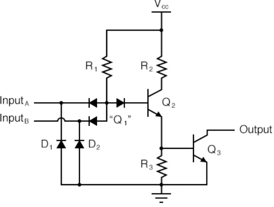
Fig: TTL NAND Gate
Specifications | TTL | CMOS |
Basic Gate | NAND | NOR/NAND |
Components | Passive Elements & Transistors | MOSFETs |
Fan-out | 10 | >50 |
Noise Immunity | Strong | Extremely Strong |
Noise Margin | Moderate | High |
TPD in ns | 1.5 to 30 | 1 to 210 |
Clock Rate in MHz | 35 | 10 |
Power/Gate in mW | 10 | 0.0025 |
Figure of Merit | 100 | 0.7 |
Gate circuits are made to sustain variations in input and output voltage levels.
Variations are usually the result of various factors.
- When Batteries lose their full potential, they cause the supply voltage to drop.
- High operating temperatures drifts transistor voltage and current characteristics.
- Spurious pulses on signal lines are introduced by normal surges of current in neighbouring supply lines.
- LNM (Low noise margin): LNM=VILmax-VOLmax.
- HNM (High noise margin): HNM=VOHmin-VIHmin
The time between the logic transition on an input and the corresponding logic transition on the output of the logic gate.
It is measured at midpoints.
- It is the number of inputs that a gate can have like a two input AND gate has fan-in of two, a three input NAND gate as a fan-in of three etc.
- Hence a NOT gate has a fan-in of one.
- The figure below shows the effect of fan-in on a CMOS based gate.
- Normally delay increases as a quadratic function of fan-in.
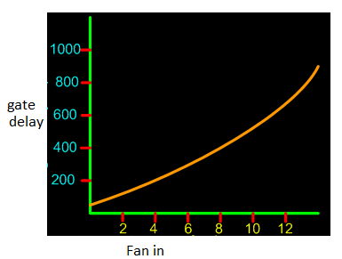
Fig: Effects of Fan-in
- The number of gates that each gate can drive, while providing voltage levels in the specified range is called the standard load or fan-out.
- It depends on the amount of electric current a gate can source or sink while driving other gates.
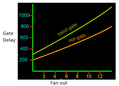
Fig: Effects of Fan-out
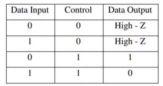
In normal logic circuits, there are two states of output, LOW and HIGH. If the output is in only either of those two states.
In complex digital systems like microcomputers and microprocessors, a number of gate outputs may be required to connect to a common line, referred to as a bus which in turn may be required to drive a number of gate inputs.
When a number of gate outputs are connected to the bus,
- Totem pole TTL outputs leads to heating of the ICs which may get damaged.
- Open-collector TTL outputs causes the problems of loading and speed of operation.
To overcome these difficulties, in addition to low impedance outputs 0 & 1, there is a third state known as the High-impedance state.
Such logic circuits in which the output can have three states is called Tri-state logic. When the gate is disabled, it is in the third state.
Emitter Coupled Logic or ECL emitter-coupled logic (ECL) is a high-speed integrated circuit bipolar transistor logic family. ECL uses an overdriven BJT differential amplifier with single-ended input and limited emitter current to avoid the saturated (fully on) region of operation and its slow turn-off behavior.
Emitter Coupled Logic (ECL), also referred to as Current Mode Logic families, is a digital technology with extremely high-speed. Transistors are not allowed to go into deep saturation thus, eliminating storage delays like in TTL logic families.

Fig: Motorola ECL 10,000 basic gate circuit diagram. Image source: Wikipedia
As the current is steered between two legs of an emitter-coupled pair, ECL is sometimes called current-steering logic (CSL), current-mode logic (CML)or current-switch emitter-follower (CSEF) logic.
ECL's major disadvantage is that each gate continuously draws current, which means that it requires (and dissipates) significantly more power than those of other logic families, especially when quiescent.
CMOS inverter
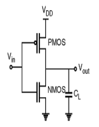
Fig: CMOS inverter
- It consists of PMOS and NMOS FET.
- The input A serves as the gate voltage for both transistors.
- The NMOS transistor has an input from Vss (ground) and PMOS transistor has an input from Vdd. The terminal Y is output.
- When a high voltage (~ Vdd) is given at input terminal (A) of the inverter, the PMOS becomes open circuit and NMOS switched OFF so the output will be pulled down to Vss.
- The truth table of inverter is:
A | Y = A’ |
0 | 1 |
1 | 0 |
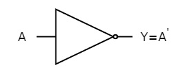
Fig: NOT gate (ref. 1)
CMOS characteristics
The VTC is divided into five regions (1-5) for easy of understanding. The above shown curve is possible when both T1 and T2 are matched for optimum operation. Optimum operation is achieved when Vin = Vdd/2 we get Vout = Vdd/2. This can be achieved by adjusting width and length of both T1 and T2 as other parameters like mobility, oxide capacitance varies between different technologies.
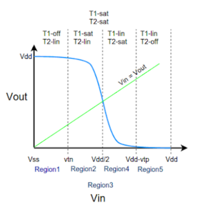
Fig: CMOS characteristics
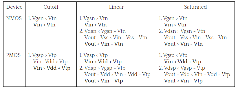
Region-1
In this, the input is in the range of (0, Vtn).
- NMOS is in cut-off as Vgs<Vtn
- PMOS is in linear as Vgsp<Vtp and Vdsp>Vgsp -Vtp.
- Zero current flows from supply voltage and the power dissipation is zero.
Region-2
Here, the input is in the range of (Vtn, Vdd/2).
- NMOS is in saturation as Vgs>Vtn and Vout>Vin – Vtn.
- PMOS is in linear region as Vdsp>Vgsp -Vtp.
- Since both the transistors are conducting some amount of current flows from supply in this region.
Region-3
Here the input voltage is Vdd/2. At this point the output voltage is Vdd/2. Here both the NMOS and PMOS are in saturation and the output drops drastically from Vdd to Vdd/2. At this point a large amount of current flows from the supply.
- NMOS is in saturation as Vgs>Vtn and Vout>Vin - Vtn.
- PMOS is in saturation as Vgsp<Vtp and Vdsp<Vgsp -Vtp.
- Large amount of current is drawn from supply and hence large power dissipation.
Region-4
In this region the input voltage is in the range of (Vdd/2, Vdd-Vtp). Here the PMOS remains in saturation as Vout< Vin - Vtp and Vgsp<Vtp. But the NMOS moves from saturation to linear region since the drain to source voltage now is less than Vgsn-Vtn.
- NMOS is in linear as Vgs>Vtn and Vout< Vin - Vtn.
- PMOS is in saturation as Vgsp<Vtp and Vdsp<Vgsp -Vtp.
- A medium amount of current is drawn as NMOS is in linear region and power dissipation is low.
Region-5
In this region the input voltage is in the range of (Vdd-Vtp, Vdd). Here the PMOS moves from saturation to cut-off as the Vgsp is so high that Vgsp>Vtp. The NMOS still remains in linear as the drain to source voltage now is less than Vgsn-Vtn.
- NMOS is in linear as Vgs>Vtn and Vout< Vin - Vtn.
- PMOS is in cut-off as Vgsp>Vtp.
- Zero current flows from the supply and hence the power dissipation is zero.
CMOS configurations- Wired Logic, Open-drain outputs
Open Drain is a type of programmable output port configuration with push pull, input only, and quasi-bidirectional configurations. Open-collector/open-drain is a circuit technique which allows multiple devices to communicate bidirectionally on a single wire. This is basically a mode which provides just a pull-down operation.
An open collector/open drain is a common type of output found on many integrated circuits (IC). Instead of outputting a signal of a specific voltage or current, the output signal is applied to the base of an internal NPN transistor whose collector is externalized (open) on a pin of the IC. The emitter of the transistor is connected internally to the ground pin. If the output device is a MOSFET the output is called open drain and it functions in a similar way.
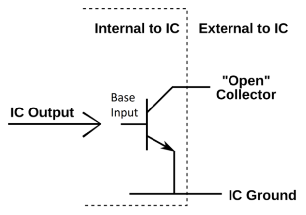
Fig: CMOS
CMOS driving TTL:
Following figure shows a CMOS gate driving N TTL gates. For such an arrangement to operate properly the following conditions are required to be satisfied,
VOH (CMOS) ≥ VIH(TTL)
VOL (CMOS) ≤ VIL(TTL)
– IOH (CMOS) ≥ NIIH(TTL)
IOL (CMOS) ≥ – NIIL(TTL)
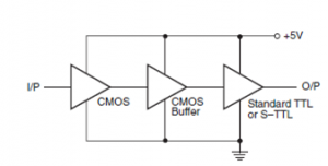
The first possible type of CMOS-to-TTL interface is the one where both ICs are operated from a common supply. We have read in earlier sections that the TTL family has a recommended supply voltage of 5 V, whereas the CMOS family devices can operate over a wide supply voltage range of 3†“18 V. In the present case, both ICs would operate from 5 V. As far as the voltage levels in the two logic states are concerned, the two have become compatible. The CMOS output has a VOH (min.) of 4.95V (for VCC =5 V) and a VOL (max.) of 0.05 V, which is compatible with VIH (min.) and VIL (max.) requirements of approximately 2 and 0.8V respectively for TTL family devices. In fact, in a CMOS-to- TTL interface, with the two devices operating on the same VCC, voltage level compatibility is always there. It is the current level compatibility that needs attention. That is, in the LOW state, the output current-sinking capability of the CMOS IC in question must at least equal the input current-sinking requirement of the TTL IC being driven. Similarly, in the HIGH state, the HIGH output current drive capability of the CMOS IC must equal or exceed the High-level input current requirement of TTL IC. For a proper interface, both the above conditions must be met. As a rule of thumb, a CMOS IC belonging to the 4000B family (the most widely used CMOS family) can feed one LS TTL or two low-power TTL unit loads. When a CMOS IC needs to drive a standard TTL or a Schottky TTL device, a CMOS buffer (4049B or 4050B) is used. 4049B and 4050B are hex buffers of inverting and noninverting types respectively, with each buffer capable of driving two standard TTL loads.
Figure below shows a CMOS-to-TTL interface with both devices operating from 5V supply and the CMOS IC driving a low-power TTL or a low-power Schottky TTL device.
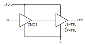
Figure below shows a CMOS-to-TTL interface where the TTL device in use is either a standard TTL or a Schottky TTL.
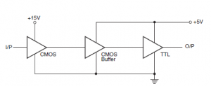
The CMOS-to-TTL interface when the two are operating on different power supply voltages can be achieved in several ways. One such scheme is shown below. In this case, there is both a voltage level as well as a current level compatibility problem.
TTL Driving CMOS:
For TTL gate driving N CMOS gates arrangement to operate properly, the following conditions are required to be satisfied:
VOH (TTL) ≥ VIH(CMOS)
VOL (TTL) ≤ VIL(CMOS)
– IOH (TTL) ≥ NIIH(CMOS)
IOL (TTL) ≥ – NIIL(CMOS)
In the TTL-to-CMOS interface, current compatibility is always there. The voltage level compatibility in the two states is a problem. VOH (min.) of TTL devices is too low as regards the VIH (min.) requirement of CMOS devices. When the two devices are operating on the same power supply voltage, that is, 5 V, a pull-up resistor of 10 k_ achieves compatibility as shown in below figure.
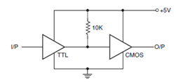
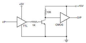
The pull-up resistor causes the TTL output to rise to about 5V when HIGH. When the two are operating on different power supplies, one of the simplest interface techniques is to use a transistor (as a switch) in-between the two, as shown below.
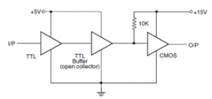
Another technique is to use an open collector type TTL buffer as shown below.
The memory is organized in the form of a cell, each cell is able to be identified with a unique number called address. Each cell is able to recognize control signals such as “read” and “write”, generated by CPU when it wants to read or write address. Whenever CPU executes the program there is a need to transfer the instruction from the memory to CPU because the program is available in memory. To access the instruction CPU generates the memory request.
Memory Request:
Memory request contains the address along with the control signals. For Example, when inserting data into the stack, each block consumes memory (RAM) and the number of memory cells can be determined by the capacity of a memory chip.
Example: Find the total number of cells in 64k*8 memory chip.
Size of each cell = 8
Number of bytes in 64k = (26)*(210)
Therefore,
The total number of cells = 216 cells
With the number of cells, the number of address lines required to enable one cell can be determined.
Word Size:
It is the maximum number of bits that a CPU can process at a time and it depends upon the processor. Word size is a fixed size piece of data handled as a unit by the instruction set or the hardware of a processor.
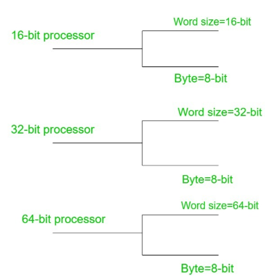
Memory can be classified as –
- Main Memory– Main memory has the disadvantage of high-cost and low-capacity storage. But its advantage or facility is the high speed of data transfer. The control unit can be able to directly communicate with the main memory. Main memory can be generally classified into random-access memory (RAM) and read-only memory (ROM). It is a volatile memory. Due to the absence of power, the content of this memory will be lost.
- Secondary Memory– Secondary memory is also frequently known as auxiliary memory. The control unit can’t directly communicate with the secondary memory. It is a non-volatile memory.
Random Access Memory (RAM) – RAM contains of a various number of memory locations wherein each location typically 8-bits are stored. It can be possible to read from a RAM location, as well as write to a RAM location. The drawback of RAM is that it is volatile. That means, when the power supply to the RAM is switched off, the information in the RAM will be lost.
From the memory, data can be accessed in two different ways – Sequential Access and Random Access.
Sequential Access − Sequential access and random access are two types of accessing information. In sequential access, it is mandatory to access information strictly in order. If there are 4000 memory locations, it has to be accessed in the order of 1, 2, 3…,4000. Thus, it takes minimum time to access information from location 0 and at most time to access information from location 4000. Magnetic Tape is an example that employs sequential access.
Random Access − In a random-access technique, it can be possible to access a memory location in any order. For example, one can read from the 4000locations in the order of 1500, 1210, 3060, 1640, 1352, and so on. Second, it takes a similar time to read from a memory location irrespective of its position. In a RAM, the access method is random, and its name, in fact, is derived based on the method of access.
Read Only Memory (ROM) – ROM consists of a number of memory locations wherein each location typically 8-bits are stored like a RAM. A ROM also uses random access method just like a RAM. The advantage of ROM is that it is non-volatile in nature.
The different versions of ROM which are provided by semiconductor manufacturers for storing information –
Mask-Programmed ROM – It derives this name because the information is written to this type of ROM at the time of manufacture by applying a suitable mask. Once the manufacturer writes this type of ROM, it cannot be possible to change this information even by the manufacturer. So that the information entered is permanent. It is cheap with compared to the other types of ROMs when the cost per unit quantity is considered.
Programmable Read Only Memory (PROM) – The user writes information to this type of ROM with the help of PROM programmer equipment. Once the user writes this type of ROM, it cannot be possible to change this information anymore. Like Mask-Programmed ROM, the information entered is permanent. Though itis cheaper than the other types of ROMs but it is costlier than a mask ROM. The user can buy even a single piece of PROM from a local shop. Thus, PROMs are implemented in equipment those are produced in small quantities.
Erasable Programmable Read Only Memory (EPROM) – Information is written to this type of ROM by the user with the help of EPROM programmer equipment. As its content is erasable and rewritable, so the user can change this information in a number of times. Thus, although the information entered is not lost when power is switched off, it can be possible to erase it and then write new information. With the exposure of strong ultraviolet (UV) light from a very close distance on the quartz window of the EPROM chip, we can erase the content of the EPROM. Then the contents of the entire EPROM are entirely lost. The user can purchase even a single piece of EPROM from the market read and write its content for several numbers of times as well.
Electrically erasable (or Alterable) Programmable Read Only Memory (EEPROM or EEPROM) − Information is has written to this type of ROM by the user with the help of EPROM programmer equipment. After the user writes this type of ROM, it can be possible to change this information a number of times.
FPGAs are based on gate array technology unlike the PROM technology of early PLDs. These devices comprise of configurable logic blocks (CLBs) along with an interconnection matrix running in-between. FPGAs work based upon the look-up tables (LUTs) and the flip-flops which form a part of CLB. The user has to program the CLBs to perform a certain logical function and then use the interconnection matrix to connect one or more logic blocks together. Further, they comprise of input-output (I/O) ports facilitating the design both from the point of programming as well as debugging.
These devices are capable of implementing state-machine based sequential designs along with the designs based on combinational logic. FPGAs are used to realize more complex designs when compared to CPLDs due to their high density. Moreover, FPGAs offer the customer the flexibility to design/re-design the logic even after being deployed in the work field which gives them the name field-programmable.
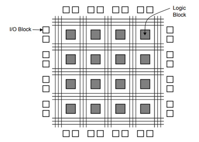
Fig: Architecture of FPGA
Programmable Logic Array
- Programmable Logic Array (PLA) is a fixed architecture logic device with programmable AND gates followed by programmable OR gates.
- It is basically a type of programmable logic device used to build reconfigurable digital circuit.
- PLDs have undefined function at the time of manufacturing but they are programmed before made into use.
- PLA is a combination of memory and logic.
- PLA is similar to a ROM in concept; however, it does not provide full decoding of variables and does not generate all min terms as in the ROM.
- It does not require any type of programming like in C and C++.
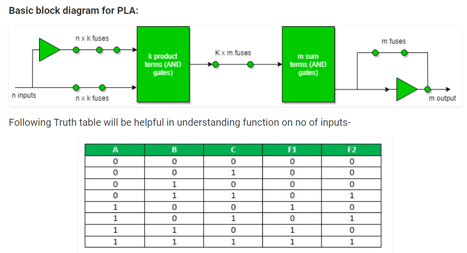
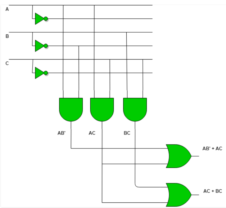
F1 = AB’C’ + AB’C + ABC’ + ABC
On simplifying we get: F1 = AB’ + AC
F2 = A’BC + AB’C + ABC
On simplifying we get: F2 = BC + AC
Applications:
- PLA is used to provide control over data path.
- PLA is used as a counter.
- PLA is used as a decoder.
- PLA is used as a BUS interface in programmed I/O.
Programmable Array Logic
- PAL stands for Programmable Array Logic.
- It is one type of PLD which is known as Programmable Logic Device circuit, and working of this PAL is the same as the PLA.
- The designing of the PAL can be done with fixed OR gates as well as programmable AND gates. By using this we can implement two easy functions wherever the associates AND gates with each OR gate denote the highest number of product conditions that can be produced in the form of SOP (sum of product) of an exact function.
- As the logic gates like AND is connected continually toward the OR gates, and that indicates that the produced product term is not distributed with the output functions.
- The major notion behind PLD development is to fabricate a compound Boolean logic onto a single chip by removing the defective wiring, avoiding the logic design, as well as decreasing the consumption of power.
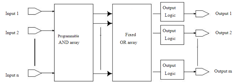
Fig: PAL architecture
Implement the following Boolean expression with the help of programmable array logic (PAL)
X =AB + AC’
Y= AB’ + BC’
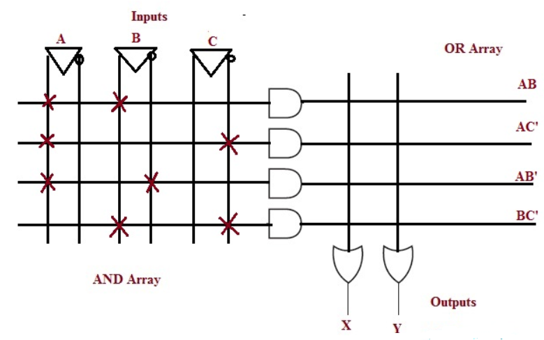
Applications:
- PAL is used as a counter.
- PAL is used as a decoder.
Comparison between PLA and PAL
Programmable Array Logic (PAL) | Programmable Logic Array (PLA) |
The full form of PAL is programmable array logic | The full form of the PLA is a programmable logic array |
The construction of PAL can be done using the programmable collection of AND & OR gates | The construction of PLA can be done using the programmable collection of AND & fixed collection of OR gates. |
The availability of PAL is less prolific | The availability of PLA is more |
The flexibility of PAL programming is more | The flexibility of PLA is less |
The cost of a PAL is expensive | The cost of PLA is middle range |
The number of functions implemented in PAL is large | The number of functions implemented in PLA is limited |
The speed of PAL is slow | The speed of PLA is high |
References:
1. R. P. Jain, "Modern Digital Electronics", McGraw Hill Education, 2009.
2. M. M. Mano, "Digital logic and Computer design", Pearson Education India, 2016.
3. A. Kumar, "Fundamentals of Digital Circuits", Prentice Hall India, 2016.