Unit – 2
Energy bands in intrinsic and extrinsic silicon
INTRINSIC SEMICONDUCTOR
An intrinsic type of semiconductor material made to be very pure chemically. As a result, it possesses a very low conductivity level having very few charge carriers, namely holes and electrons, which it possesses in equal quantities.
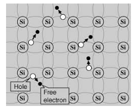
Figure 1: Intrinsic Semiconductor
The most commonly used semiconductor basics material by far is silicon. Silicon has four valence electrons in its outermost shell which it shares with its neighbouring silicon atoms to form a full orbital of eight electrons. The structure of the bond between the two silicon atoms is such that each atom shares one electron with its neighbour making the bond very stable.
As there are very few free electrons available to move around the silicon crystal, crystals of pure silicon (or germanium) are therefore good insulators. Silicon atoms are arranged in a definite symmetrical pattern making them a crystalline solid structure. A crystal of pure silica (silicon dioxide or glass) is generally said to be an intrinsic crystal (it has no impurities) and therefore has no free electrons.
An extremely pure semiconductor is called an Intrinsic Semiconductor. Based on the energy band phenomenon, an intrinsic semiconductor at absolute zero temperature is shown below.
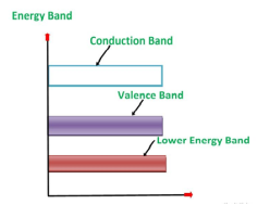
Figure 2: Intrinsic semiconductor at absolute zero temperature.
Its valence band is filled and the conduction band is empty. When the temperature is raised and some heat energy is supplied to it, some of the valence electrons are lifted to the conduction band leaving behind holes in the valence band as shown below.
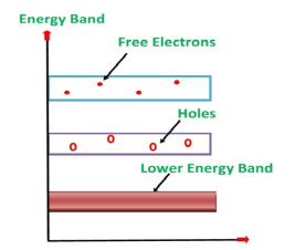
Figure 3: Intrinsic semiconductor at T >0
A hole is the absence of an electron in a particular place in an atom. Although it is not a physical particle in the same sense as an electron, a hole can be passed from atom to atom in a semiconductor material. It is considered to have a positive charge. Holes are positive charge carriers.
The electrons reaching the conduction band move randomly. The holes created in the crystal also free to move anywhere.
This behaviour of the semiconductor shows that they have a negative temperature coefficient of resistance. This means that with the increase in temperature, the resistivity of the material decreases, and the conductivity increases.
But simply connecting a silicon crystal to a battery supply is not enough to extract an electric current from it. To do that we need to create a “positive” and a “negative” pole within the silicon allowing electrons and therefore electric current to flow out of the silicon. These poles are created by doping the silicon with certain impurities.
DOPING
The process by which an impurity is added to a semiconductor is known as Doping. The amount and type of impurity which is to be added to the material have to be closely controlled during the preparation of extrinsic semiconductor. Generally, one impurity atom is added to 108 atoms of a semiconductor.
The purpose of adding impurity in the semiconductor crystal is to increase the number of free electrons or holes to make it conductive.
If a Pentavalent impurity, having five valence electrons is added to a pure semiconductor a large number of free electrons will exist. Which makes an n-type extrinsic semiconductor.
If a trivalent impurity having three valence electrons is added, a large number of holes will exist in the semiconductor. Which makes a p-type extrinsic semiconductor.
EXTRINSIC SEMICONDUCTOR
Extrinsic types of semiconductors are those where a small amount of impurity has been added to the basic intrinsic material. This 'doping' uses an element from a different periodic table group and in this way, it will either have more or fewer electrons in the valence band than the semiconductor itself. This creates either an excess or shortage of electrons. In this way two types of semiconductors are available: Electrons are negatively charged carriers. Holes are positively charged carriers.
Depending upon the type of impurity added the extrinsic semiconductor may be classified as an n-type semiconductor and p-type semiconductor.
P-TYPE EXTRINSIC SEMICONDUCTOR
The extrinsic p-Type Semiconductor is formed when a trivalent impurity is added to a pure semiconductor in a small amount, and as a result, a large number of holes are created in it. A large number of holes are provided in the semiconductor material by the addition of trivalent impurities like Gallium and Indium. Such type of impurities which produce a p-type semiconductor is known as an Acceptor Impurities because each atom of them creates one hole which can accept one electron.
In a P-type semiconductor material, there is a shortage of electrons, i.e. there are 'holes' in the crystal lattice. Electrons may move from one empty position to another and in this case, it can be considered that the holes are moving. This can happen under the influence of a potential difference and the holes can be seen to flow in one direction resulting in an electric current flow. It is harder for holes to move than for free electrons to move and therefore the mobility of holes is less than that of free electrons. Holes are positively charged carriers.
A trivalent impurity like Aluminium, having three valence electrons is added to Silicon crystal in a small amount. Each atom of the impurity fits in the Silicon crystal in such a way that its three valence electrons form covalent bonds with the three surrounding Silicon atoms as shown in the figure below.
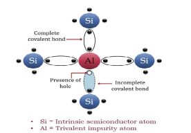
Figure 4: p-Type Semiconductor
ENERGY BAND DIAGRAM OF P-TYPE SEMICONDUCTOR
The energy band diagram of a p-Type Semiconductor is shown below.
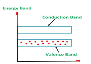
Figure 5: Energy band diagram of a p-Type Semiconductor
A large number of holes or vacant space in the covalent bond is created in the crystal with the addition of the trivalent impurity. A small or minute quantity of free electrons is also available in the conduction band.
They are produced when thermal energy at room temperature is imparted to the Silicon crystal-forming electron-hole pairs. But the holes are more in number as compared to the electrons in the conduction band. It is because of the predominance of holes over electrons that the material is called a p-type semiconductor. The word “p” stands for positive material.
CONDUCTION THROUGH P TYPE SEMICONDUCTOR
In p-type semiconductors, a large number of holes are created by the trivalent impurity. When a potential difference is applied across this type of semiconductors.
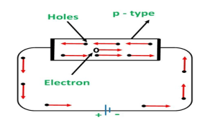
Figure 6: Conduction through p type semiconductor
The holes are available in the valence band are directed towards the negative terminal. As the current flow through the crystal is by holes, which are a carrier of positive charge, therefore, this type of conductivity is known as positive or p-type conductivity. In a p-type conductivity, the valence electrons move from one covalent to another.
The conductivity of an n-type semiconductor is nearly double that of a p-type semiconductor. The electrons available in the conduction band of the n-type semiconductor are much more movable than holes available in the valence band in a p-type semiconductor. The mobility of holes is poor as they are more bound to the nucleus.
Even at room temperature, the electron-hole pairs are formed. These free electrons which are available in minute quantity also carry a little amount of current in the p-type semiconductors.
N-TYPE EXTRINSIC SEMICONDUCTOR
When a few Pentavalent impurities such as Phosphorus whose atomic number is 15, which is categorized as 2, 8, and 5. It has five valence electrons, which are added to silicon crystals. Each atom of the impurity fits in four silicon atoms as shown in the figure below.
Hence, each Arsenic atom provides one free electron in Silicon crystal. Since an extremely small amount of Phosphorus, impurity has a large number of atoms; it provides millions of free electrons for conduction.
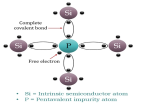
Figure 7: N-type semiconductor
An N-type semiconductor material has an excess of electrons. In this way, free electrons are available within the lattices, and their overall movement in one direction under the influence of a potential difference results in an electric current flow. This is an N-type semiconductor, the charge carriers are electrons.
ENERGY DIAGRAM OF N-TYPE SEMICONDUCTOR
A large number of free electrons are available in the conduction band because of the addition of the Pentavalent impurity. These electrons are free electrons that did not fit in the covalent bonds of the crystal. However, a minute quantity of free electrons is available in the conduction band forming hole- electron pairs.
The Energy diagram of the n-type semiconductor is shown in the figure below.
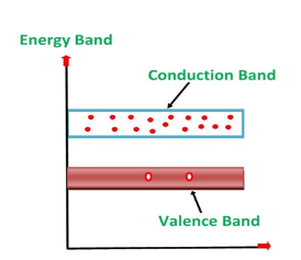
Figure 8: Energy diagram of the n-type semiconductor
- The addition of pentavalent impurity results in a large number of free electrons.
- When thermal energy at room temperature is imparted to the semiconductor, a hole-electron pair is generated and as a result, a minute quantity of free electrons is available. These electrons leave behind holes in the valence band.
- Here n stands for negative material as the number of free electrons provided by the pentavalent impurity is greater than the number of holes.
Any motion of free carriers in a semiconductor leads to a current. This motion can be caused by an electric field due to an externally applied voltage, since the carriers are charged particles. We will refer to this transport mechanism as carrier drift. In addition, carriers also move from regions where the carrier density is high to regions where the carrier density is low. This carrier transport mechanism is due to the thermal energy and the associated random motion of the carriers. We will refer to this transport mechanism as carrier diffusion. The total current in a semiconductor equals the sum of the drift and the diffusion current.
As one applies an electric field to a semiconductor, the electrostatic force causes the carriers to first accelerate and then reach a constant average velocity, v, due to collisions with impurities and lattice vibrations. The ratio of the velocity to the applied field is called the mobility. The velocity saturates at high electric fields reaching the saturation velocity. Additional scattering occurs when carriers flow at the surface of a semiconductor, resulting in a lower mobility due to surface or interface scattering mechanisms.
Diffusion of carriers is obtained by creating a carrier density gradient. Such gradient can be obtained by varying the doping density in a semiconductor or by applying a thermal gradient.
Both carrier transport mechanisms are related since the same particles and scattering mechanisms are involved. This leads to a relationship between the mobility and the diffusion constant called the Einstein relation.
Examples
Q) Determine thermal equilibrium of electron and hole concentration for an n-type silicon semiconductor at T=300oK where ND = 1x1016cm-3 and NA =0. Assume ni = 1.5 x 1010cm-3?
Sol: The majority carrier concentration
n0 = ½ {(ND- NA) + (ND- NA)2+4ni2)1/2}
n0 = 1016 cm-3
The minority carrier concentration
p0 = ni2/ND
p0 = 2.25x x104 cm-3
Q) Determine thermal equilibrium of electron and hole concentration for doping concentration at T=300oK where ND = 4x1013cm-3 and NA =0. Assume ni = 2.4 x 1013cm-3?
Sol: The majority carrier concentration
n0 = ½ {(ND- NA) + (ND- NA)2+4ni2)1/2}
n0 =3.12x1013 cm-3
The minority carrier concentration
p0 = ni2/ND
p0 = 1.45x x1013 cm-3
Q) Determine thermal equilibrium of electron and hole concentration in n-type semiconductor at T=300oK where ND = 2x1016cm-3 and NA =12x1015 cm-3. Assume ni = 1.5 x 1010cm-3?
Sol: The majority carrier concentration
n0 = ½ {(ND- NA) + (ND- NA)2+4ni2)1/2}
n0 =4x1015 cm-3
The minority carrier concentration
p0 = ni2/ND
p0 = 11.25x x103 cm-3
Drift current Definition: The flow of electric current due to the motion of charge carriers under the influence of external electric field is called drift current.
When an electric field E is applied across a semiconductor material, the charge carriers attain a drift velocity vd
So drift velocity vd =μ.E
The relation between current density J and drift velocity vd is
J = Nqvd
Where N is the carrier concentration
q is the charge of electron or hole
From equations (1) and (2), we get
Jdrift = Nq μE
μ is the mobility of charge carrier.
The above equation shows the general expression for drift current density. Drift current density due to electrons is
Je(drift) = neμeE
Where n is the electrons carrier concentration
And μe is the mobility of electrons.
Drift current density due to holes is
Jh(drift) = peμhE
Where p is the carrier concentration of holes.
μh is the mobility of holes
So Total drift current density
Jdrift (total) = Je(drift) + Jh(drift) = neμeE + peμhE
= eE (nμe+pμh )
Diffusion current
Definition: The flow of electric current due to the motion of charge carriers under concentration gradient is called diffusion current
Or
The motion of charge carriers from the region of higher concentration to lower concentration leads to a current called diffusion current.
Let ∆N be the excess electron concentration. Then according to Fick’s law, the rate of diffusion of charge carriers is proportional to concentration gradient
Rate of diffusion of charge ∝ -
= - D
Where D is the diffusion coefficient of charge carriers.
The negative sign indicates decrease of N with increase of x So,
The diffusion current density Jdiffu is
Jdiffu = - qD
Where q is the charge of the charge carrier
Diffusion current density due to holes is
Jdiffu (hole) = - eDh
Diffusion current density due to electrons is (as electron carry negative charge so we will get +sign here.
Jdiffu (electrons) = eDe
Jdiffu (total) = Jdiffu (hole) + Jdiffu (electrons)
Jdiffu (total) = - eDh + eDe
+ eDe
The expression for total current density due to holes is
Jh (total) = Jh(drift) + Jdiffu (hole) = peμhE - eDh
The expression for total current density due to electrons is
Je (total) = Je(drift) + Jdiffu (electrons) = neμeE + eDe
Key Takeaways
- In case of semiconductors we observe two kinds of currents; Drift current and Diffusion current.
- The flow of electric current due to the motion of charge carriers under the influence of external electric field is called drift current. STotal drift current density is given by
Jdrift (total) = Je(drift) + Jh(drift) = eE (nμe+pμh )
3. The flow of electric current due to the motion of charge carriers under concentration gradient is called diffusion current. Total current density due to electrons is given by
Je (total) = Je(drift) + Jdiffu (electrons) = neμeE + eDe
Diffusion current | Drift current |
Diffusion current occurs even though there isn’t an electric field applied to the semiconductor | Drift current depends on the electric field applied on the p-n junction diode.
|
It depends constant Dp and Dn, and +q and –q , for holes and electrons respectively but it is independent of permittivity.
| It depends upon permittivity.
|
Direction of the diffusion current depends on the change in the carrier concentrations.
| Direction of the drift current depends on the polarity of the applied field.
|
Examples
Q1) For a p-type Ge ni = 2.1x10¹⁹m-3 density of boron =3.2x10²³ atoms m-3. The electron and hole mobility are 0.4 and 0.2 m2V-1s-1. Calculate conductivity before and after addition of boron?
Sol: Before adding boron
 = q (p
 p+n
p+n n)
n)
= ni q ( p+
p+ n) = 2.1x1019x1.6x10-19x(0.4+0.2)=2.016 S/m-1
After adding boron
 = q p
= q p p
p
= 3.2x1023x1.6x10-19x0.2=10.24x10³S/m-1
Q2) Determine the density of the donor atoms which have been added to the intrinsic Ge to make it a n-type material of resistivity 0.1x10⁻²ohm-m. Mobility of electron in n-type semiconductor is 0.5m2V-1s-1.
Sol:  = q (n
 n)
n)
n=  /q
/q n
n
 = 1/
= 1/
n= 1/ q
q n = 1/(0.1x10-2x0.5x1.6x10-19) = 1.25x10²²m-3
Q3) The intrinsic carrier density at room temperature in Ge is 3.4x10¹⁹m-3. If electron and hole mobilities are 0.4 and 0.2 m2V-1s-1 respectively. Calculate its resistivity?
Sol:  = 1/
= 1/
 =ni q (
 p+
p+ n) = 3.4x1019x 1.6x10-19(0.4+0.2) = 3.264S/m-1
 = 1/
= 1/ = 1/3.264 = 0.31ohm-m
Q4) The electron and hole mobilities in In-Sb are 6 and 0.2 m2V-1s-1 respectively. At room temperature resistivity of In-Sb is 2x10⁻⁴ohm-m. Find intrinsic carrier concentration assuming the material to be intrinsic?
Sol:  = 1/
= 1/
 =ni q (
 p+
p+ n)
n)
ni = 1/  q (
q ( p+
p+ n) = 1/2x10-4x1.6x10-19(6+0.2) = 5.04x10²¹m-3
Q5) An electric field of 90Vm-1 is applied to n-type semiconductor. Determine the current density in sample given electron mobility 0.4 m2V-1s-1, n=5.9x10²⁰m-3?
Sol: J= E
E
 = nq
= nq n = 5.9x1020x1.6x10-19x0.4=37.36S/m-1
J=3.39x10³
Q6) Determine the density of the donor atoms which have been added to the intrinsic Ge to make it a n-type material of resistivity 0.5x10⁻²ohm-m. Mobility of electron in n-type semiconductor is 0.8m2V-1s-1.
Sol:  = q (n
 n)
n)
n=  /q
/q n
n
 = 1/
= 1/
n= 1/ q
q n = 1/(0.5x10-2x0.8x1.6x10-19) = 1.56x10²¹m-3
Q7) Calculate the drift current density in a semiconductor for a given electric field. For germanium sample at T=300oK where ND = 0 and NA =1x1015 cm-3 ni = 2.4x1013 cm-3. Assume electron and hole mobility to be 3900 cm2/V-sec and 1900 cm2/V-sec. Applied electric field is E= 40V/cm?
Sol: As NA>>ND
p0 = ½ {(NA- ND) + (NA- ND)2+4ni2)1/2}
p0 = 5x1014cm-3
n= ni2/NA
n= 5.76x1011cm-3
J = q (p p+n
p+n n) E
n) E
For extrinsic p-type semiconductor
J = q NA p E =1.6x10-19x1900x1015x40 =12.16 A/cm2
MOBILITY
The drift velocity produced per unit electric field is called 'mobility' , Thus Mobility is obviously a central parameter in characterizing electron and hole transport due to drift.

The word mobility refers to freedom of movement. Analogously, in semiconductor work the mobility parameter is a measure of the ease of carrier motion in a crystal. Increasing the motion-impeding collisions within a crystal decreases the mobility of the carriers.
In other words, the carrier mobility varies inversely with the amount of scattering taking place within the semiconductor.
Lattice scattering involving collisions with thermally agitated lattice atoms, and ionized impurity (i.e., donor-site and/or acceptor-site) scattering. Relative to lattice scattering, it should be emphasized that it is the thermal vibration, the displacement of lattice atoms from their lattice, positions, that leads to carrier scattering. The internal field associated with the stationary array of atoms in a crystal is already taken into account in the effective mass formulation.

Where  is the mean free time between collisions and m* is the conductivity effective mass.
However, μ is also noted to vary inversely with the carrier effective mass—lighter carriers move more readily.
The carrier mobilities are essentially independent of the doping concentration. For dopings in excess of l015/cm3, the mobilities monotonically decrease with increasing NA or ND.
The mobilities of carrier depend upon temperature as . For Electrons
  and for holes
RESISTIVITY
Resistivity is an important material parameter that is closely related to carrier drift. Qualitatively, resistivity is a measure of a material's inherent resistance to current flow—a "normalized" resistance that does not depend on the physical dimensions of the material.
Quantitatively, resistivity (p) is defined as the proportionality constant between the electric field impressed across a homogeneous material and the total particle current per unit area flowing in the material; that is,
E =ρJ ………… (1)
Or
J = E = ………… (2)
Where = 1/ρ is the material conductivity. In a homogeneous material J= Jdrift and as established with the help of Eqs. (1) and (2), it therefore follows that
Jdrift = JN(drift) + JP(drift) ………… (3)
 ………… (4)
In a non-degenerate donor-doped semiconductor maintained in the extrinsic temperature region where ND >> ni, ni ND and p = ni2/ND << n.
Thus, for typical dopings and mobilities,  ND in an n-type semiconductor. Similar arguments yield
  NA in a p-type semiconductor. Consequently, under conditions normally encountered in Si samples maintained at or near room temperature, Eq. (3.7) simplifies to
 for n-type semiconductor
And
 for p-type semiconductor.
One of the most common methods of measuring a material‘s surface resistivity is using either the two-or four-point probe method .Two probe method is used to measure the resistivity of films with fairly large resistance. But if the film resistance is very small (comparable with the lead) four probe method is adopted.
Both two and four probe methods are the most popular methods for measuring resistivity due to the ability of minimizing the parasitic effects of contact resistance, Rc shown below in equation (1). Let us illustrate four probes method
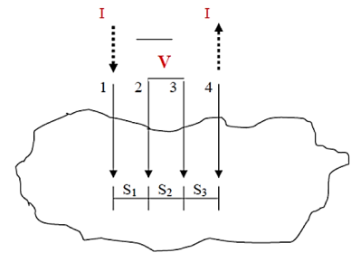
Figure 9: Four-point probe test setup. Probes 1 and 4 carry current (I), 2 and 3 measure voltage (V).
In the four-point probe setup as shown in figure 16, the voltage potential V adjacent to a probe carrying current can be given by:
V = ρI/ 2πr ………….(2)
Where ρ is the surface resistivity of a material of semi-infinite size, I is the current in the probe, and r is the distance between the voltage measurement and the current probe.
A very convenient way to measure the sheet resistance of a film is to press a 4-point metal tip probe assembly in to the surface as shown in (figure 2). The outer probe is connected to current source and inner probes to detect the voltage drop.
Voltage at probe number 2 is
 …………(3)
Voltage at probe number 3 is
 …………(4)
Hence the total voltage is V
 .………..(5)
The resistivity
 .………..(6)
If all the probes are equidistant with inner probe distance S then the equation reduces to
 .………..(7)
Most surface resistivity measurements of semiconductor wafers or thin films are made on a small surface area substrate. Small spacing differences in probe spacing can cause the resistivity values to vary widely across a sample surface. A high quality four-point head is necessary to get repeatable and reliable resistivity values. When measuring samples with low resistivity, high currents are needed in the current probes to obtain good voltage readings.
Resistance and Resistivity are both pristine, beautiful science words. Sheet Resistance (Rs) is a dirty, uncultured engineering word — it exists only to make calculations easier, because thinking too hard may kill an engineer. Engineers are notorious for their shortcuts, because all they care about is lame stuff like “accomplishing things” or “making tangible progress.” Not us scientists. Anyways, sheet resistance has units of Ohms per square.
Sheet Resistance is a combination of resistivity of a material and its shape, and is a shortcut for calculating resistance when designing PCBs.
If you have the sheet resistance Rs, all you need is the ratio of length (L) to width (W) to find the resistance, like so:
R= Rs x L/W
DC sheet resistance
The "DC" explanation of sheet resistance ignores skin depth. For resistor calculations, 99% of the time this is a reasonable approximation. For attenuation in metal traces at microwave frequencies, this assumption will lead you astray, and you need to read our content on RF sheet resistance.
Bulk resistivity is the property which is independent of frequency and geometry. In microwaves, often we are dealing with thin films of conductors, which have been applied at a controlled thickness. A more convenient property to deal with in this case is sheet resistance. The sheet resistance of a metal film is often expressed in ohms/square.
R=
Where:
 = bulk resistivity
L= length of the resistor
w = width of the resistor
t = thickness of the resistor
Sheet resistance, Rsh, is equal to bulk resistivity divided by thickness. It can be used to conveniently calculate resistance values from number of squares, as follows:
Resistance = Rsh x number of squares
Rsh = sheet resistance = 
Number of squares = L/w
Examples
Q1) The resistance of a wire is 20 Ω. What will be new resistance, if it is stretched uniformly 8 times its original length?
Sol: R1 = 20 Ω, R2=?
Let the original length (l1) be l.
The new length, l2 = 8l1 (i.e) l2 =8l
The original resistance, R = ρ [ l1 / A1]
The new resistance

Though the wire is stretched, its volume is unchanged.
Initial volume = Final volume
A1l1= A2l2 , A1l = A28l
A1 / A2 = 8l / l = 8
By dividing equation R2 by equation R1, we get


Substituting the value of A1/A2, we get
R2 / R1 = 8 ×8 = 64 2
R2 = 64 × 20=1280 Ω
Hence, stretching the length of the wire has increased its resistance.
Q2) Consider a rectangular block of metal of height A, width B and length C as shown in the figure.
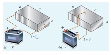
If a potential difference of V is applied between the two faces A and B of the block (figure (a)), the current IAB is observed. Find the current that flows if the same potential difference V is applied between the two faces B and C of the block (figure (b)). Give your answers in terms of IAB.
Solution
In the first case, the resistance of the block

The current 
In the second case, the resistance of the block 
The current 
To express interms of
  we multiply and divide equation (2) by AC we get

Since C>A, the current 
Q3) Compute the resistivity of the given material whose resistance is 2 Ω; area of cross-section and length are 25cm2 and 15 cm respectively?
Answer:
Given
R = 2 Ω
l = 15 cm = 0.15 m
A = 25 cm2 = 0.25 m2
Resistivity formula is


Q4) The length and area of wire are given as 0.2 m and 0.5 m2 respectively. The resistance of that wire is 3 Ω, calculate the resistivity?
Sol:
Given
R = 3 Ω
l = 0.2 m and
A = 0.5 m2
Resistivity formula is


There are many thousands of different Types of Resistors and are produced in a variety of forms because their particular characteristics and accuracy suit certain areas of application, such as High Stability, High Voltage, High Current etc, or are used as general-purpose resistors where their characteristics are less of a problem.
Some of the common characteristics associated with the resistor are; Temperature Coefficient, Voltage Coefficient, Noise, Frequency Response, Power as well as a resistors Temperature Rating, Physical Size and Reliability.
All modern fixed value resistors can be classified into four broad groups:
- Carbon Composition Resistor – Made of carbon dust or graphite paste, low wattage values.
- Film or Cermet Resistor – Made from conductive metal oxide paste, very low wattage values
- Wire-wound Resistor – Metallic bodies for heatsink mounting, very high wattage ratings
- Semiconductor Resistor – High frequency/precision surface mount thin film technology
Carbon Resistors are the most common type of Composition Resistors. Carbon resistors are a cheap general purpose resistor used in electrical and electronic circuits. Their resistive element is manufactured from a mixture of finely ground carbon dust or graphite (similar to pencil lead) and a non-conducting ceramic (clay) powder to bind it all together.
The Carbon Composite Resistor is a low to medium type power resistor which has a low inductance making them ideal for high frequency applications but they can also suffer from noise and stability when hot. Carbon composite resistors are generally prefixed with a “CR” notation (eg, CR10kΩ ) and are available in E6 ( ± 20% tolerance (accuracy) ), E12 ( ± 10% tolerance) and E24 ( ± 5% tolerance) packages with power ratings from 0.250 or 1/4 of a Watt up to 5 Watts.
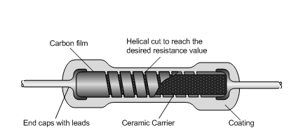
Fig 10 Carbon composite resistor
Film Type Resistors
This resistor consists of Metal Film, Carbon Film and Metal Oxide Film resistor types, which are generally made by depositing pure metals, such as nickel, or an oxide film, such as tin-oxide, onto an insulating ceramic rod or substrate.
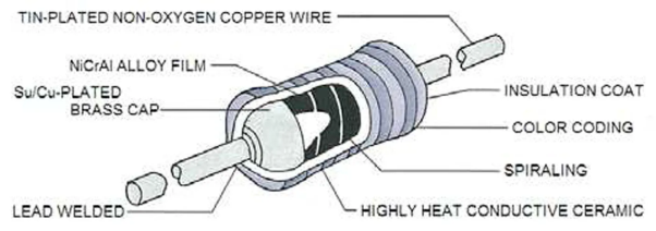
Fig 11 Film Resistor
The resistive value of the resistor is controlled by increasing the desired thickness of the deposited film giving them the names of either “thick-film resistors” or “thin-film resistors”. Once deposited, a laser is used to cut a high precision spiral helix groove type pattern into this film. The cutting of the film has the effect of increasing the conductive or resistive path, a bit like taking a long length of straight wire and forming it into a coil.
Metal Film Resistors have much better temperature stability than their carbon equivalents, lower noise and are generally better for high frequency or radio frequency applications. Metal Oxide Resistors have better high surge current capability with a much higher temperature rating than the equivalent metal film resistors.
Another type of film resistor commonly known as a Thick Film Resistor is manufactured by depositing a much thicker conductive paste of CERamic and METal, called Cermet, onto an alumina ceramic substrate.
Metal Film Resistors are prefixed with a “MFR” notation (eg, MFR100kΩ) and a CF for Carbon Film types. Metal film resistors are available in E24 (±5% & ±2% tolerances), E96 (±1% tolerance) and E192 (±0.5%, ±0.25% & ±0.1% tolerances) packages with power ratings of 0.05 (1/20th) of a Watt up to 1/2 Watt.
Wire wound Type of Resistor
Another type of resistor, called a Wire wound Resistor, is made by winding a thin metal alloy wire (Nichrome) or similar wire onto an insulating ceramic former in the form of a spiral helix similar to the film resistor above.
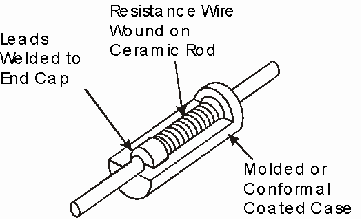
Fig 12 Wire wound Resistor
These types of resistors are generally only available in very low ohmic high precision values (from 0.01Ω to 100kΩ) due to the gauge of the wire and number of turns possible on the former making them ideal for use in measuring circuits and Wheatstone bridge type applications.
Wire wound resistor types are prefixed with a “WH” or “W” notation (eg WH10Ω) and are available in the WH aluminium clad package (±1%, ±2%, ±5% and ±10% tolerance) or the W vitreous enamelled package (±1%, ±2% and ±5% tolerance) with power ratings from 1W to 300W or more.
Calculating Resistor Values by colour Code
The Resistor Colour Code system is all well and good but we need to understand how to apply it in order to get the correct value of the resistor. The “left-hand” or the most significant coloured band is the band which is nearest to a connecting lead with the colour coded bands being read from left-to-right as follows:
Digit, Digit, Multiplier = Colour, Colour x 10 colour in Ohm’s (Ω)
For example, a resistor has the following coloured markings;
Yellow Violet Red = 4 7 2 = 4 7 x 102 = 4700Ω or 4k7 Ohm.
The fourth and fifth bands are used to determine the percentage tolerance of the resistor. Resistor tolerance is a measure of the resistors variation from the specified resistive value and is a consequence of the manufacturing process and is expressed as a percentage of its “nominal” or preferred value.
Typical resistor tolerances for film resistors range from 1% to 10% while carbon resistors have tolerances up to 20%. Resistors with tolerances lower than 2% are called precision resistors with the or lower tolerance resistors being more expensive.
Most five band resistors are precision resistors with tolerances of either 1% or 2% while most of the four band resistors have tolerances of 5%, 10% and 20%. The colour code used to denote the tolerance rating of a resistor is given as:
Brown = 1%, Red = 2%, Gold = 5%, Silver = 10 %
If resistor has no fourth tolerance band then the default tolerance would be at 20%
Number of Coloured Bands | 3 Coloured Bands (E6 series) | 4 Coloured Bands (E12 series | 5 Coloured Bands (E48 series | 6 Coloured Bands (E96 series |
1st Brand | 1st digit | 1st digit | 1st digit | 1st digit |
2nd Brand | 2nd digit | 2nd digit | 2nd digit | 2nd digit |
3rd Brand | Multiplier | Multiplier | 3rd digit | 3rd digit |
4th Brand | - | Tolerance | Multiplier | Multiplier |
5th Brand | - | - | Tolerance | Tolerance |
6th Brand | - | - | - | Temperature coefficient |
Resistor Colour Code Table
Colour | Digit | Multiplier | Tolerance |
Black | 0 | 1 |
|
Brown | 1 | 10 |  |
Red | 2 | 100 |  |
Orange | 3 | 1,000 |
|
Yellow | 4 | 10,000 |
|
Green | 5 | 1,00,000 |  |
Blue | 6 | 1,000,000 |  |
Violet | 7 | 10,000,000 |  |
Grey | 8 |
|  |
White | 9 |
|
|
Gold |
| 0.1 |  |
Silver |
| 0.01 |  |
None |
|
|  |
References:
1. G. Streetman, and S. K. Banerjee, “Solid State Electronic Devices,” 7th edition, Pearson,2014.
2. D. Neamen, D. Biswas, "Semiconductor Physics and Devices," McGraw-Hill Education.
3. S. M. Sze and K. N. Kwok, “Physics of Semiconductor Devices,” 3rd edition, John Wiley & Sons, 2006.
4. C.T. Sah, “Fundamentals of Solid State Electronics,” World Scientific Publishing Co. Inc,1991.
5. Y. Tsividis and M. Colin, “Operation and Modeling of the MOS Transistor,” Oxford univ. Press, 2011.
6. Muhammad H. Rashid, “Electronic Devices and Circuits,” Cengage publication, 2014.