Unit – 3
Generation and recombination of carriers
Carrier generation is a process where electron-hole pairs are created by exciting an electron from the valence band of the semiconductor to the conduction band, thereby creating a hole in the valence band.
Recombination is the reverse process where electrons from the conduction and holes from valence band recombine and are annihilated.
These processes must conserve both quantized energy and momentum, and the vibrating lattice plays a large role in conserving momentum.
- Recombination and generation are always happening in semiconductors both optically and thermally.
- Their rates are in balance at equilibrium.
- If the product of the rate becomes greater than the recombination rate, again driving the system back towards equilibrium.
- As the electron and hole densities is a constant at equilibrium, maintained by recombination and generation occurring at equal rates.
- When there is a surplus of carriers the rate of recombination becomes greater than the rate of generation, driving the system back towards equilibrium.
In semiconductors several different processes exist which lead to recombination, the most important ones are:
1) Band-to-band recombination
2) Auger generation/recombination
3) Surface recombination
1) Band-to-band recombination or Radiative recombination
Band-to-band recombination or Radiative recombination is the reverse process of photon absorption, where an electron drops back down to its equilibrium energy band and radiates a photon.
It is the process of electrons jumping down from the conduction band to the valence band in a radiative manner.
During band-to-band recombination the energy absorbed by a material is released in the form of photons. Generally, these released photons contain the same or less energy than those initially absorbed.
The photon emitted may have the energy of the band gap difference or less, depending on how much energy is lost in the mechanism
Radiative recombination plays a more major role in direct band semiconductors.
The total radiative recombination rate, given below as R, is proportional to the product of the concentration of occupied states (electrons, n) in the conduction band and that of the unoccupied states in the valence band (holes, p)
R= Bnp
Band-to-band recombination depends on the density of available electrons and holes. Both carrier types need to be available in the recombination process. Therefore, the rate is expected to be proportional to the product of n and p. Also, in thermal equilibrium, the recombination rate must equal the generation rate since there is no net recombination or generation. As the product of n and p equals ni2 in thermal equilibrium, the net recombination rate can be expressed as:
U= B(np-ni2)
Where B is the bimolecular recombination constant for a given semiconductor. It can be calculated from the semiconductor’s absorption coefficient. ni2 is the familiar “intrinsic carrier concentration”
2. Auger recombination Auger recombination involves three particles: an electron and a hole, which recombine in a band-to-band transition and give off the resulting energy to another electron or hole. The expression for the net recombination rate is therefore similar to that of band-to-band recombination but includes the density of the electrons or holes, which receive the released energy from the electron-hole annihilation.
In other words Auger recombination the energy is given to a third carrier which is excited to a higher energy level without moving to another energy band.
After the interaction, the third carrier normally loses its excess energy to thermal vibrations. Since this process is a three-particle interaction, it is normally only significant in non-equilibrium conditions when the carrier density is very high.
Auger recombination is most important at high carrier concentrations caused by heavy doping. In silicon-based solar cells, Auger recombination limits the lifetime and ultimate efficiency.
The more heavily doped the material is, the shorter the Auger recombination lifetime.
3. Surface recombination
Recombination at surfaces and interfaces can have a significant impact on the behavior of semiconductor devices.
Areas of defect, such as at the surface of solar cells where the lattice is disordered, recombination is very high.
This is because surfaces and interfaces typically contain a large number of recombination centers because of the abrupt termination of the semiconductor crystal, which leaves a large number of electrically active states.
In addition, the surfaces and interfaces are more likely to contain impurities since they are exposed during the device fabrication process.
The net recombination rate due to trap-assisted recombination and generation is given by:

The recombination is due to a two-dimensional density of traps, Nts, as the traps only exist at the surface or interface.
Understanding the impacts and the ways to limit surface recombination leads to better and more robust solar cell designs. Surface recombination is high in solar cells, but can be limited.
Key Takeaways
- Carrier generation is a process where electron-hole pairs are created by exciting an electron from the valence band of the semiconductor to the conduction band, thereby creating a hole in the valence band.
- Recombination is the reverse process where electrons from the conduction and holes from valence band recombine and are annihilated.
- These processes must conserve both quantized energy and momentum, and the vibrating lattice plays a large role in conserving momentum.
- Recombination and generation are always happening in semiconductors both optically and thermally. Their rates are in balance at equilibrium.
- In semiconductors several different processes exist which lead to recombination, the most important ones are: Band-to-band recombination, Auger generation/recombination and Surface recombination
Poisson’s Equation:
From the Gauss’s law in the point form Poisson’s equation can be derived. Consider the Gauss’s law in the point form as
 .
.  =
= 
 = flux density
 Volume charge density.
For a homogeneous isotropic and linear medium, flux density and the electric field are directly proportional. Thus,
 =
=  .
. 
 .
.  .
.  =
= 
From the gradient relationship
E = -  . V
. V
 .
.  (-
(-  . V) =
 (
(  .
.  V) =
V) = 
 .
.  V) =-
V) =-  /
/ 
Now  .
.  operation is called ‘del squared’ operation denoted as
  2.
2.
 2. V = -
  /
/ 
This equation is called as Poisson’s Equation
Continuity Equations
Each and every type of carrier action—whether it be drift, diffusion, indirect or direct thermal recombination, indirect or direct generation, or some other type of carrier action—gives rise to a change in the carrier concentrations with time. The combined effect of all types of carrier action can therefore be taken into account by equating the overall change in the carrier concentrations per unit time  or
or  to the sum of the time
  or
or  due to the individual processes; that is,

 ……… (1)
The overall effect of the individual processes is established by applying the requirement of conservation of carriers. Electrons and holes cannot mysteriously appear and disappear at a given point, but must be transported to or created at the given point via some type of on-going carrier action. There must be a spatial and time continuity in the carrier concentrations.
For this reason, Eqs. (1) are known as the continuity equations. The continuity equations can be written in a somewhat more compact form by noting

 ……… (2)
Equations (2), which can be established by a straightforward mathematical manipulation, merely state that there will be a change in the carrier concentrations within a given small region of the semiconductor if an imbalance exists between the total carrier currents into and out of the region.
Using Eqs. (2), we obtain

 ……… (3)
The (3) continuity equations are completely general and directly or indirectly constitute the starting point in most device analyses.
In computer simulations the continuity equations are often employed directly. The continuity equations are typically utilized only in an indirect fashion.
A P-N Junction Diode is formed by doping one side of a piece of silicon with a P-type dopant (Boron) and the other side with a N-type dopant (phosphorus). Ge can be used instead of Silicon. The P-N junction diode is a two-terminal device. This is the basic construction of the P-N junction diode. It is one of the simplest semiconductor devices as it allows current to flow in only one direction.
ZERO BIASED CONDITION
In this case, no external voltage is applied to the P-N junction diode; and therefore, the electrons diffuse to the P-side and simultaneously holes diffuse towards the N-side through the junction, and then combine with each other. Due to this an electric field is generated by these charge carriers. The electric field opposes further diffusion of charged carriers so that there is no movement in the middle region. This region is known as depletion width or space charge.
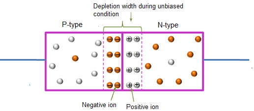
Figure: Unbiased or zero biased PN Junction Diode
FORWARD BIAS
In the forward bias condition, the positive terminal of the battery is connected to the P-Type material and the negative terminal of the battery is connected to the N-type material. This connection is also called as giving positive voltage.
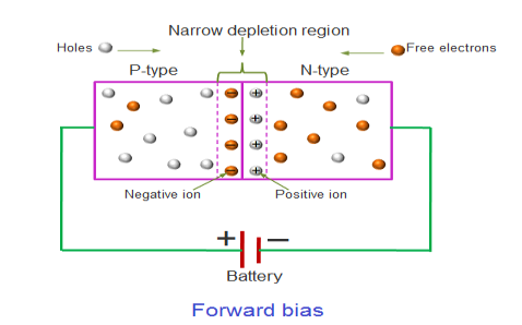
Figure: Forward Bias
Electrons from the N-region cross the junction and enters the P-region. Due to the attractive force that is generated in the P-region the electrons are attracted and move towards the positive terminal. Simultaneously the holes are attracted to the negative terminal of the battery. By the movement of electrons and holes current flows. In this condition, the width of the depletion region decreases due to the reduction in the number of positive and negative ions.
If this external voltage Vf becomes greater than the value of the potential barrier, approx. 0.7 volts for silicon and 0.3 volts for germanium, the potential barriers opposition will be overcome and current will start to flow.
This is because the negative voltage pushes or repels electrons towards the junction giving them the energy to cross over and combine with the holes being pushed in the opposite direction towards the junction by the positive voltage. This results in a characteristics curve of zero current flowing up to this voltage point, called the “knee” on the static curves and then a high current flow through the diode with little increase in the external voltage as shown in I-V characteristics.
REVERSE BIAS
In the forward bias condition, the negative terminal of the battery is connected to the N-type material and the positive terminal of the battery is connected to the P-type material. This connection is also known as giving positive voltage. Hence, the electric field due to both the voltage and depletion layer is in the same direction. This makes the electric field stronger than before. Due to this strong electric field, electrons and holes want more energy to cross the junction so they cannot diffuse to the opposite region. Hence, there is no current flow due to the lack of movement of electrons and holes.
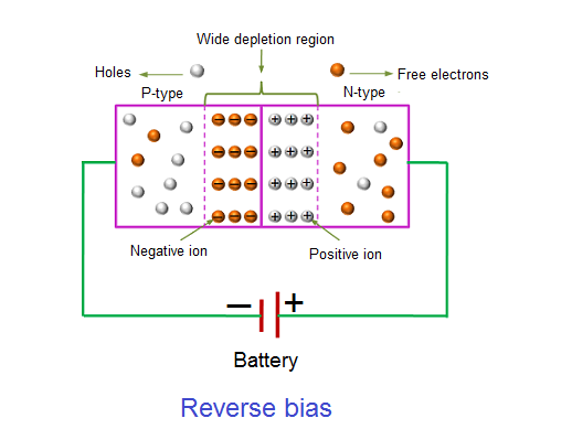
Figure: Reverse Bias
The positive voltage applied to the N-type material attracts electrons towards the positive electrode and away from the junction, while the holes in the P-type end are also attracted away from the junction towards the negative electrode.
The net result is that the depletion layer grows wider due to a lack of electrons and holes and presents a high impedance path, almost an insulator. The result is that a high potential barrier is created thus preventing current from flowing through the semiconductor material.
This condition represents a high resistance value to the PN junction and practically zero current flows through the junction diode with an increase in bias voltage. However, a very small leakage current does flow through the junction which can be measured in micro-amperes, ( μA ).
If the reverse bias voltage Vr applied to the diode is increased to a sufficiently high enough value, it will cause the diode’s PN junction to overheat and fail due to the avalanche effect around the junction. This may cause the diode to become shorted and will result in the flow of maximum circuit current, and this shown as a step downward slope in the reverse static characteristics curve in I-V characteristics.
The I-V Characteristic Curves, which is short for Current-Voltage Characteristic Curves or simply I-V curves of an electrical device
The application of a forward biasing voltage on the junction diode results in the depletion layer becoming very thin and narrow which represents a low impedance path through the junction thereby allowing high currents to flow. The point at which this sudden increase in current takes place is represented on the static I-V characteristics curve above as the “knee” point. The current starts increasing with increase in voltage. At knee voltage current shows a sharp increment in its magnitude. This behaviour us mentioned above. As large current flow in forward biasing so we measure this current in mA.
When a junction diode is Reverse Biased, the thickness of the depletion region increases and the diode acts like an open circuit blocking current flow. So only a very small leakage current will flow.
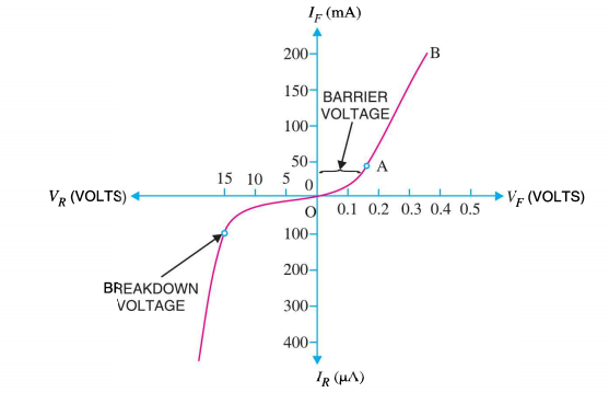
Figure: I-V Characteristics
The hybrid two port model is shown below.
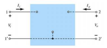
Fig: Hybrid model
Vi = h11Ii + h12Vo
Io = h21Ii + h22Vo
h11 = hi = Vi/Io for Vo =0 [Input resistance]
h12 = hr = Vi/Vo for Ii =0 [Reverse voltage gain]
h21 = hf = Io/Ii for Vo =0 [forward current gain]
h22 = ho = Io/Vo for Ii =0 [output admittance]
The hybrid equivalent model is shown below

Fig: Equivalent hybrid model
The transistor model has three terminals with two ports.
hi = input resistance
ho= output conductance
hr= Vi/Vo = reverse transfer voltage
hf= Io/Ii = forward transfer current ratio
The simplified model is shown below
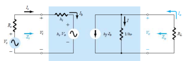
Fig: Simplified Model
Finding current gain Ai
Applying KCL at the output of above circuit
Io =I + hf Ib = Vo ho + hf Ib
Vo = -Io RL
Io = -Io RL ho + hf Ib
Io (1 + RL ho) = hf Ib
Ai = Io/ Ib = hf/(1 + RL ho)
Finding Voltage Gain AV
Applying KVL at input of the above h-model
Vi = hi Ib + hr Vo
But Ib = (1 + ho RL)/hf
Io = - Vo/RL
Substituting in above equation and solving for Vo/Vi we get
Av = - hf RL/hi + (hi ho- hf hr) RL
Finding Input Impedance Zi
Vi = hi Ib + hr Vo
Io = - Vo/RL
Ai = Io/ Ib
Vi = hi Ib - hrRLAiIb
Zi = Vi/Ib = hi - hrRLAi
Finding Output impedance Zo
It is ratio of output voltage to output current with Vs =0
Io = Voho + hfIb
Ii = -hrVo/Rs + hi
Zo = Vo/Io = 1/[ho – (hfhr/hi+ Rs)]
Key takeaway
CE to CB h-parameters | CE to CC h-parameters | CE h-parameters to r-parameters |
 |  |  |
 |  |  |
 |  |  |
 |  |   |
Example
Consider the small-signal amplifier shown in Figure 1. Assume VCC = 24 V, RS = 1.5 kΩ, R1 = 8.6 kΩ, R2 = 200 kΩ, RC = 5 kΩ, RL = 2 kΩ, β = 75, and π = 750 Ω. Draw the small-signal equivalent circuit and find the voltage gain of the amplifier?
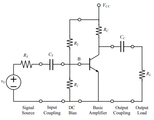
Sol: All capacitors are replaced by short circuit. The voltage source vS and its internal resistance RS are replaced by a current source (vS/RS) according to Source Transformation theorem

Consider the circuit in stage one, first.
Let us find the equivalent resistance of the four resistors: 1.5, 200, 8.6, and 0.75


Stage one circuit will turn into the following circuit
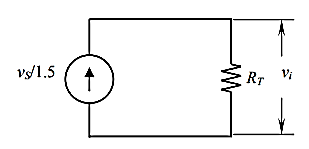

This value of vi is same across each element in the circuit of Figure 3. Now, apply ohm’s law to find ib

Now, consider stage two circuit

Accordingly, the gain is vout / vS = – 44.6. The (-) sign is an indication for the counter clockwise direction of current in stage-two circuit.
Small Signal Analysis of CE Amplifiers
In most practical cases it is appropriate to obtain approximate values of AV, Ai etc rather than calculating exact values. How the circuit can be modified without greatly reducing the accuracy. Figure shows the CE amplifier equivalent circuit in terms of h-parameters Since 1 / hoe in parallel with RL is approximately equal to RL if 1 / hoe >> RL then hoe may be neglected. Under these conditions.
Ic = hfe IB.
hre vc = hre Ic RL = hre hfe Ib RL
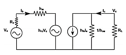
Fig: CE Amplifiers
Since hfe hre » 0.01, this voltage may be neglected in comparison with hic Ib drop across hie provided RL is not very large. If load resistance RL is small than hoe and hre can be neglected.
Ai = Io/ Ib = hfe/(1 + RL hoe)
Ri= hie
Av= AIRL/Ri= -hfe RL/hie
Output impedance seems to be infinite. When Vs = 0, and an external voltage is applied at the output we fined Ib = 0, IC = 0. True value depends upon RS and lies between 40 K and 80K. On the same lines, the calculations for CC and CB can be done.
CE amplifier with an emitter resistor:
The voltage gain of a CE stage depends upon hfe. This transistor parameter depends upon temperature, aging and the operating point. Moreover, hfe may vary widely from device to device, even for same type of transistor. To stabilize voltage gain AV of each stage, it should be independent of hfe. A simple and effective way is to connect an emitter resistor Re as shown in figure. The resistor provides negative feedback and provide stabilization.
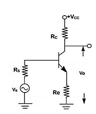
Fig: CE amplifier with an emitter resistor
Current gain Ai = IL/Ib = Ic/ Ib = - hfeIb/Ib
Input Resistance is given by
Ri= Vi/Ib
= hie Ib +(1+hfe)IbRe/Ib
= hie +(1+hfe) Re
The input resistance is increased by (1+hfe) Re


CE amplifiers are very popular to amplify the small signal ac. After a transistor has been biased with a Q point near the middle of a dc load line, ac source can be coupled to the base. This produces fluctuations in the base current and hence in the collector current of the same shape and frequency. The output will be enlarged sine wave of same frequency. The amplifier is called linear if it does not change the wave shape of the signal.
As long as the input signal is small, the transistor will use only a small part of the load line and the operation will be linear. On the other hand, if the input signal is too large. The fluctuations along the load line will drive the transistor into either saturation or cut off. This clips the peaks of the input and the amplifier is no longer linear.
The CE amplifier configuration is shown
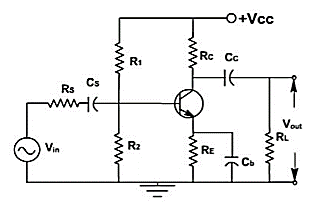
Fig: CE Amplifier Circuit
The coupling capacitor (CC) passes an ac signal from one point to another. At the same time, it does not allow the dc to pass through it. Hence it is also called blocking capacitor.
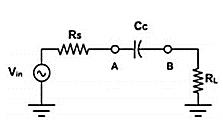
Fig: Coupling Capacitor
From Figure above the ac voltage at point A is transmitted to point B. For this series reactance XC should be very small compared to series resistance RS. The circuit to the left of A may be a source and a series resistor or may be the Thevenin equivalent of a complex circuit. Similarly, RL may be the load resistance or equivalent resistance of a complex network. The current in the loop is given by

As frequency increases, XC decreases, and current increases until it reaches to its maximum value vin / R. Therefore, the capacitor couples the signal properly from A to B when XC<< R. The size of the coupling capacitor depends upon the lowest frequency to be coupled. Normally, for lowest frequency XC 0.1R is taken as design rule. The coupling capacitor acts like a switch, which is open to dc and shorted for ac. The bypass capacitor Cb is similar to a coupling capacitor, except that it couples an ungrounded point to a grounded point. The Cb capacitor looks like a short to an ac signal and therefore emitter is said ac grounded. A bypass capacitor does not disturb the dc voltage at emitter because it looks open to dc current. As a design rule XCb =0.1RE at
Analysis of CE amplifier: In a transistor amplifier, the dc source sets up quiescent current and voltages. The ac source then produces fluctuations in these current and voltages. The simplest way to analyse this circuit is to split the analysis in two parts: dc analysis and ac analysis. One can use superposition theorem for analysis.
Characteristics of Common Emitter Amplifier
(i) The current gain Ai is high for RL < 10 kΩ.
(ii) The voltage gain is high for normal values of load resistance RL.
(iii) The input resistance Ri is medium.
(iv) The output resistance Ro is moderately high.
Applications: CE amplifier is widely used for amplification
Common Base Amplifier
The common base amplifier circuit is shown in Figure below. The VEE source forward biases the emitter diode and VCC source reverse biased collector diode. The ac source vin is connected to emitter through a coupling capacitor so that it blocks dc.
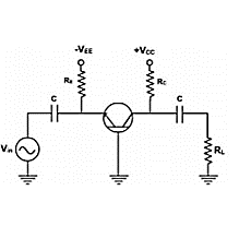
Fig: CB Amplifier
This ac voltage produces small fluctuation in currents and voltages. The load resistance RL is also connected to collector through coupling capacitor so the fluctuation in collector base voltage will be observed across RL. The dc equivalent circuit is obtained by reducing all ac sources to zero and opening all capacitors. The dc collector current is same as IE and VCB is given by VCB = VCC - IC RC. Figure above.
These current and voltage fix the Q point. The ac equivalent circuit is obtained by reducing all dc sources to zero and shorting all coupling capacitors. r'e represents the ac resistance of the diode as shown in Figure below.
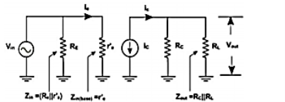
Fig: Equivalent CB Amplifier
The above figure shows the diode curve relating IE and VBE. In the absence of ac signal, the transistor operates at Q point (point of intersection of load line and input characteristic). When the ac signal is applied, the emitter current and voltage also change. If the signal is small, the operating point swings sinusoidally about Q point (A to B).
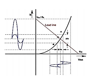
Fig: Q-Point
If the ac signal is small, the points A and B are close to Q, and arc A B can be approximated by a straight line and diode appears to be a resistance given by

If the input signal is small, input voltage and current will be sinusoidal but if the input voltage is large then current will no longer be sinusoidal because of the non-linearity of diode curve. The emitter current is elongated on the positive half cycle and compressed on negative half cycle. Therefore, the output will also be distorted. r'e is the ratio of ΔVBE and Δ IE and its value depends upon the location of Q. Higher up the Q point small will be the value of r' e because the same change in VBE produces large change in IE. The slope of the curve at Q determines the value of r'e. From calculation it can be proved that
r'e = 25mV / IE
Characteristics of Common Base Amplifier
(i) Current gain is less than unity and its magnitude decreases, with the increase of load resistance RL
(ii) Voltage gain AV is high for normal values of RL
(iii) The input resistance Ri is the lowest of all the three configurations, and
(iv) The output resistance Ro is the highest of all the three configurations.
Applications The CB amplifier is not commonly used for amplification purpose. It is used for
(i) Matching a very low impedance source
(ii) As a non-inverting amplifier to voltage gain exceeding unity.
(iii) For driving a high impedance load. (iv)As a constant current source. Common Collector Amplifier
(i) For low RL (< 10 kΩ), the current gain Ai is high and almost equal to that of a CE amplifier.
(ii) The voltage gain AV is less than unity.
(iii) The input resistance is the highest of all the three configurations.
(iv) The output resistance is the lowest of all the three configurations.
Applications The CC amplifier is widely used as a buffer stage between a high impedance source and a low impedance load.
Key takeaway
Quantity | CB | CC | CE |
 | 0.98 | 47.5 | -46.5 |
 | 131 | 0.989 | -131 |
 | 128.38 | 46.98 | 6091.5 |
 | 22.6 | 144 k | 1065 |
 | 1.72 M | 80.5 | 45.5 k |

Effects of RS and RL on CE amplifier operation
Voltage Amplification Factor (Avs) taking into account the resistance (Rs) of the source
This overall voltage gain Avs is given by
Avs = V2 / VS = V2 V1 / V1VS = Av V1/ VS
From the equivalent input circuit using Thevenin’s equivalent for the source shown in Figure
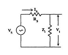
Fig: Thevenin’s Equivalent
V1 = VS Zi / (Zi + RS)
V1 / VS = Zi / (Zi + RS)
Then, Avs = Av Zi / (Zi + RS)
Substituting Av = Ai ZL / Zi
Avs = Ai ZL / (Zi + RS)
Avs = Ai ZL RS / (Zi + RS) RS
Avs = Ais ZL / RS
Avs = (AI RL/Zi) * (Zi/Rs + ZL) = (AI RL/Rs + Zi)
Effect due to RL
If Rs= 0
Then,
Avs = (AI RL/Zi)
Current Amplification (Ais) taking into account the source Resistance (RS)
The modified input circuit using Norton’s equivalent circuit for the calculation of Ais is shown in Figure.
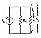
Fig: Norton Equivalent
Overall Current Gain,
Ais = -I2 / IS = - I2I1 /I1
IS = Ai I1/IS
From Figure
I1= IS RS / (RS + Zi)
I1 / IS = RS / (RS + Zi)
And hence, Ais = Ai RS / (RS + Zi)
Key takeaway
The current gain becomes
Ais = Ai RS / (RS + Zi)
Effect due to RL
If Rs= 0
Then,
Avs = (AI RL/Zi)
Emitter Follower
This is also called as common collector amplifier. It is basically used to provide current gain and for impedance matching. The circuit is shown below where the input is applied through base and output is obtained from emitter. The voltage gain is always<1 and output voltage are in phase with input voltage. The output follows the input hence it is called as emitter follower.
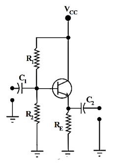
Fig: Emitter Follower
The base voltage can be obtained by applying voltage division rule on R2 and R1
VB =  VCC
VCC
The emitter voltage is VE = VB – 0.7
The emitter current is IE = 
VCEQ = VCC-VE
For A.C analysis the circuit can be drawn as shown below
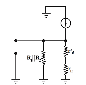
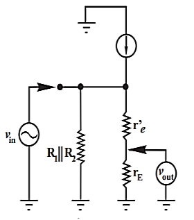
Fig: A.C equivalent circuit
The total equivalent ac emitter resistance is rE which is
rE = RE||RL
- The voltage gain AV = rE/(re’ +rE)
Practically re’ << rE. The voltage gain then becomes
AV = 1
- Current Gain Ai = hfe (Zin rE/Zbase RL)
This relationship is due to the current divisions that occur in both the input and output circuits. We have used in place of hfe. We are assuming that is approximately equal to hfe. The subscript “c” merely indicates that the parameter applies to the emitter follower (common collector) rather than the common emitter amplifier. The exact equation for hfc is
hfc = hfe +1
Since is normally much greater than 1, we normally assume that they are approximately equal.
- Input Impedance Zin = R1||R2||Zbase
- Base Input Impedance Zbase = hfe (re’+rE)
Where:
hfe= transistor current gain
re’= the ac emitter resistance
rE = RL||RE
- Output Impedance (Zout)
The output impedance is the impedance that the circuit presents to its load. When a load is connected to the circuit, the output impedance of the circuit acts as the source impedance for that load.
Zout = RE|| [re’ + (Rin’/hfe)]
Key takeaway
The voltage gain is always<1 and output voltage are in phase with input voltage. The output follows the input hence it is called as emitter follower.
Solved Examples
Q1. The voltage gain of an amplifier without feedback is 3000. Calculate the voltage gain of the amplifier if negative voltage feedback is introduced in the circuit. Given that feedback fraction mv = 0.01.
Sol:


Q2. The overall gain of a multistage amplifier is 140. When negative voltage feedback is applied, the gain is reduced to 17.5. Find the fraction of the output that is feedback to the input.
Sol:

Let  be the feedback fraction. Voltage gain with negative feedback is


Q3. When negative voltage feedback is applied to an amplifier of gain 100, the
overall gain falls to 50.
(i) Calculate the fraction of the output voltage feedback.
(ii) If this fraction is maintained, calculate the value of the amplifier gain required if the overall stage gain is to be 75.
Solution:
(i) Gain without feedback, 
Gain with feedback, 
Let  be the fraction of the output voltage feedback.

(ii) 


Q4. With a negative voltage feedback, an amplifier gives an output of 10 V with an input of 0.5 V. When feedback is removed, it requires 0.25 V input for the same output. Calculate (i) gain without feedback (ii) feedback fraction mv.
Sol:
Gain without feedback, 
Gain with feedback, 
Let  be the fraction of the output voltage feedback.

(i) Gain without feedback, 
(i) Gain with feedback, 
Now 


Q5. The gain of an amplifier without feedback is 50 whereas with negative voltage feedback, it falls to 25. If due to ageing, the amplifier gain falls to 40, find the percentage reduction in stage gain (i) without feedback and (ii) with negative feedback.
Sol:


(i) Without feedback.
The gain of the amplifier without feedback is 50. However, due to ageing it falls to 40.
 %age reduction in stage gain
(ii) With negative feedback
When the gain without feedback was 50, the gain with negative feedback was 25. Now the gain without feedback falls to 40.
 New gain with negative feedback
 % age reduction in stage gain
Q6. An amplifier has a voltage amplification Av and a fraction mv of its output is feedback in opposition to the input. If mv = 0.1 and Aν = 100, Calculate the percentage change in the gain of the system if Aν falls 6 db due to ageing.
Sol:


Fall in gain=6db
Let  be the new absolute voltage gain without feedback.


 age change in system gain
Q7. An amplifier has a voltage gain of 500 without feedback. If a negative feedback is applied, the gain is reduced to 100. Calculate the fraction of the output fed back. If, due to ageing of components, the gain without feedback falls by 20%, calculate the percentage fall in gain with feedback.
Sol:


Q8. An amplifier has an open-loop gain Av = 100,000. A negative feedback of 10 db is applied. Find (i) voltage gain with feedback (ii) value of feedback fractionmv.
Sol:
 voltage gain without feedback

Voltage gain with feedback=100-10=90db
Now 


(ii) 


Q9. An amplifier with an open-circuit voltage gain of 1000 has an output resistance of 100 Ω and feeds a resistive load of 900 Ω. Negative voltage feedback is provided by connecting a resistive voltage divider across the output and one-fiftieth of the output voltage is feedback in series with the input signal. Determine the voltage gain with negative feedback.

Sol: Voltage gain of the amplifier without feedback is:


Q10. An amplifier is required with a voltage gain of 100 which does not vary by more than 1%. If it is to use negative feedback with a basic amplifier the voltage gain of which can vary by 20%, determine the minimum voltage gain required and the feedback factor.
Sol:

Also 

Multiplying eq(i) by  we have

Substracting [(ii)-(iii)], we have
19.8=0.008
Putting the value of 


Q11. An amplifier has a gain of 1000 without feedback and cut-off frequencies are f1 = 1.5 kHz and f2 = 501.5 kHz. If 1% of output voltage of the amplifier is applied as negative feedback, what are the new cut-off frequencies?
Sol:

The new lower cut-off frequency with feedback is

The new upper cut-off frequency with feedback is

Q12. The current gain of an amplifier is 200 without feedback. When negative
current feedback is applied, determine the effective current gain of the amplifier. Given that current attenuation mi = 0.012.
Sol:

Here 

Q13. For the emitter follower circuit shown in Figure, find the input impedance.
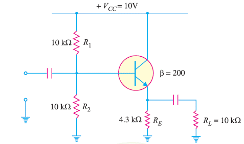
Sol:
Voltage across 
Voltage across 
Emitter current, 
 A.C. Emitter resistance,
Effective external emitter resistance is


 Input impedance of the emitter follower is


Q14) For the emitter follower circuit shown in Figure, find the input impedance.
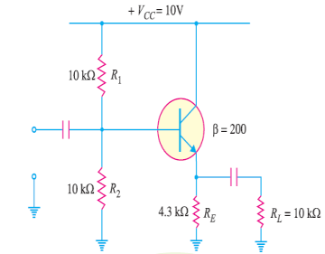
Sol:
Voltage across 
Voltage across 
 Emitter current,
 A.C emitter resisitance
Effective external emitter resistance is


 Input impedance of the emitter follower is


Q15) For the Darlington amplifier in Figure, find (i) the d.c. Levels of both the
transistors and (ii) a.c. Emitter resistances of both transistors.
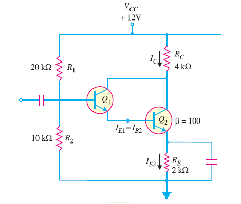
Sol:
(i) D.C Bias Levels
Base voltage of 
Emitter voltage of 
Emitter voltage of 

(ii) A.C Analysis
A.C emitter resistance of 
A.C emitter resistance of 
Q16) Calculate the value of resistor RC so that the voltage gain of the amplifier in fig is 100. Capacitors C1, C2, and C3 may be assumed short at signal frequency.
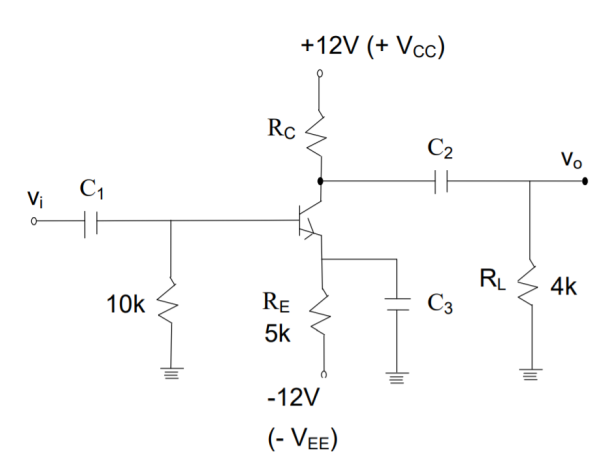
Sol:
In case, RE is by-passed, the voltage gain Av of the amplifier is,

Where rc is the effective (ac) resistance seen by the collector of the transistor, and ' e r is the dynamic resistance of the emitter. We know,


Where resistances have been taken in kΩ. Therefore,

As  (given),
  is,
is,


Q17) Find out the smallest value of load RL in the amplifier circuit shown in fig so that the voltage gain is at least 40. The dynamic emitter resistance of the transistor is 25 Ω. The coupling and by-pass capacitors may be assumed short at signal frequency.
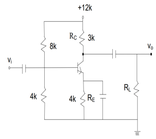
Sol:
The voltage gain of the common emitter amplifier with resistor RE by-passed (see fig.) is expressed as

Where rc is effective ac impedance seen by the collector Which, is


Q18) The silicon transistor in the common- base amplifier has the current gain α of 0.98. Find the input impedance and voltage gain of the amplifier in fig. (VBE = 0.7V)
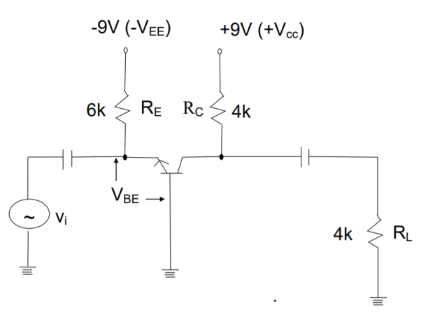
Sol: The dc voltage sources have to be grounded for ac analysis of the amplifier. Then the input impedance of the CB amplifier (in fig.) is

Where r’e is dynamic emitter resiatance and r’e << RE

Where IE is dc emitter current in the circuit

 Thus, the input impedance Zi(amp) is,

The low value of input impedance is the main reason for limited applications of CB amplifier. The voltage gain of CB amplifier is expressed as,
Since, 
Then, 
Q19) The transistor in the amplifier circuit shown in fig, has h – parameters, hie = 2kΩ and hfl = 80. The values of hoe and hre are negligible. Calculate the voltage gain and input impedance Zi(amp) of the amplifier. Capacitors C1, C2, and C3 may be assumed short at signal frequency due to small impedances.
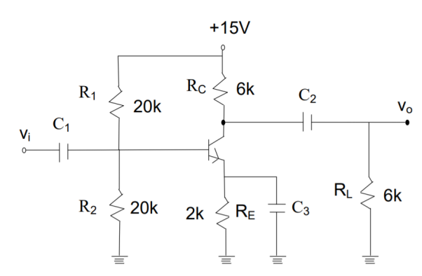
Sol: The magnitude of voltage gain with h-parameters hoe and hre dropped, and emitter resistance RE by-passed by capacitor C3 is

Because the ac load at collector, Zl, is

Further, the impedance between base and ground, Zi(base) is,

And, input impedance of amplifier, Zi(amp) is


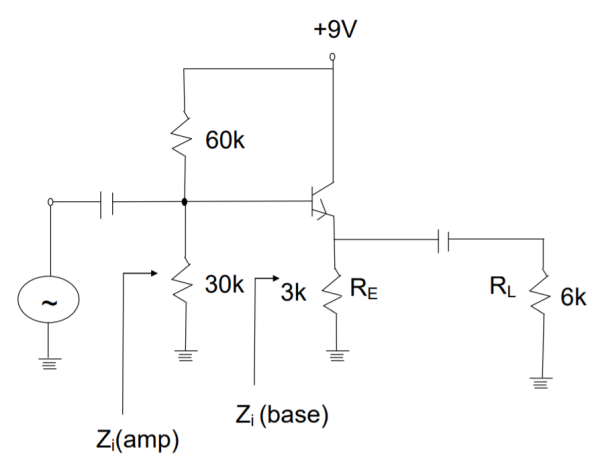
Q20) The emitter follower (common collector amplifier) shown in fig. Uses a transistor with h-parameters hie = 4.5 kΩ, hfe = 120. Other parameters hoe and hre have negligible effect on amplifier performance. Calculate voltage gain and input impedance of the amplifier. The coupling and by-pass capacitors may be assumed short at signal frequency.
Sol:
Neglecting the effect of hoe and hre on amplifier performance, the voltage gain of emitter follower may be expressed as,

Where Ze is the effective load seen by the emitter, and it is

And using hfc ≈ hfe and hic = hie,


The input impedance as seen at the base w.r.t ground is,

The input impedance of the amplifier (that is, after taking the effect of biasing resistors)

And the effective base resistance RB is,


References:
1. G. Streetman, and S. K. Banerjee, “Solid State Electronic Devices,” 7th edition, Pearson,2014.
2. D. Neamen, D. Biswas, "Semiconductor Physics and Devices," McGraw-Hill Education.
3. S. M. Sze and K. N. Kwok, “Physics of Semiconductor Devices,” 3rd edition, John Wiley & Sons, 2006.
4. C.T. Sah, “Fundamentals of Solid State Electronics,” World Scientific Publishing Co. Inc,1991.
5. Y. Tsividis and M. Colin, “Operation and Modeling of the MOS Transistor,” Oxford univ. Press, 2011.
6. Muhammad H. Rashid, “Electronic Devices and Circuits,” Cengage publication, 2014.