Unit 1
Diode circuits
The schematic symbol for a diode is as shown in figure
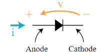
Figure 1. Diode
The black arrow ▶ in the symbol points in the direction of the diode's forward current, i the direction where current flow happens. The diode voltage v is oriented with a + sign on the end where the forward current comes into the diode.
Key Take-Aways:
- The basic symbol of a diode
- Its Representation
Voltage Amplifier
The purpose of a voltage amplifier is to make the amplitude of the output voltage waveform greater than that of the input voltage waveform.
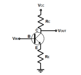
Figure 2Voltage Amplifier
A voltage amplifier circuit is a circuit that amplifies the input voltage to a higher voltage. So, for example, if we input 1V into the circuit, we can get 10V as output if we set the circuit for a gain of 10.
Current Amplifier
A current amplifier circuit is a circuit that amplifies the input current by a fixed factor and feeds it to the succeeding circuit. A current amplifier is somewhat similar to a voltage buffer but the difference is that an ideal voltage buffer will try to deliver whatever current required by the load while keeping the input and output voltages the same, where a current amplifier supplies the succeeding stage with a current that is a fixed multiple of the input current. A current amplifier can be realized using transistors.
The schematic of a current amplifier circuit using transistors is shown in the figure below.
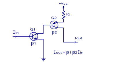
Figure 3. Current Amplifier
Two transistors are used in this circuit. β1 and β2 are the current gains of transistors Q1 and Q2 respectively. Iin is the input current, Iout is the output current and +Vcc is the transistor T2’s collector voltage
The equation for the output current is Iout = β1 β2 Iin .
Trans-conductance Amplifier
A transconductance amplifier converts an input of voltage to an output of current. It is also called a current to a voltage converter or I to V converter. It is called transconductance because the efficiency of the amplifier is measured in units of conductance.
Transconductance amplifiers are classified into two types. They are transconductance amplifiers with a floating load and transconductance amplifiers with a grounded load.
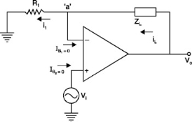
Figure 4. Transconductance amplifier with the floating load.
In the ideal op-amp,
Va = Vi -----------------------------------------(1)
And
IB1 = IB2 =0 --------------------------------(2)
Writing Kirchhoff's Current Law at node ' a' yields
IL + IB1 = i1
IL = i1 -----------------------------------------(3)
|
|
Write the equation for current through R 1:
i1 = Va-0/R1
i1 = Va/R1
Substitute equation (1) here:
i 1 = Vi/R1 -------------------------------(4)
|
|
Substitute equation (4) in (3),
IL = Vi/R1 ----------------------------------------(5)
|
|
Trans-resistance Amplifier
A trans resistance amplifier converts an input of current to an output of voltage. It is also called a voltage to current converter or V to I converter. It is called trans resistance because the efficiency of the amplifier is measured in units of resistance.
The analysis is done assuming ideal op-amp characteristics. The current entering the op-amp terminals is zero. Accordingly, the current coming from the source will essentially flow through Rf.
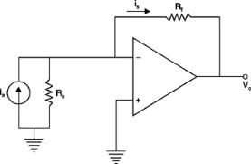
Figure 5.Transresistance amplifier.
The voltage difference between the two input terminals is zero. Since the voltage at the non-inverting input terminal is zero, the voltage at the inverting input terminal is zero.
Current through feedback resistance Rf can be calculated.
Is= Voltage difference/ Rf
= (0-Va/Rf)-----------------------------------(1)
-Vo = is Rf --------------------------------------------(2)
Vo = -is Rf ----------------------------------------------------(3)
|
|
Therefore, the output voltage is proportional to the input current.
Key Take-Aways:
- A voltage amplifier is to make the amplitude of the output voltage waveform greater than that of the input voltage waveform.
- The current amplifier amplifies the input current by a fixed factor and feeds it to the succeeding circuit.
- A transconductance amplifier converts an input of voltage to an output of current.
- A trans resistance amplifier converts an input of current to an output of the voltage
- Biasing of BJT
Biasing refers to the application of dc voltages to establish a fixed level of current and voltage. The proper flow of zero signal collector current and maintenance of proper collector-emitter voltage for the passage of signal is called Transistor Biasing. The circuit which provides transistor biasing is called the Biasing circuit.
The need for a biasing circuit is that if a signal of low voltage is given as input it has to amplify and meet these two conditions:
- The input voltage should exceed the cut-in voltage for the transistor to be ON.
- BJT should be in the active region to be operated as an amplifier.
Transistor Regions Operation:
- Linear-region operation:
Base–emitter junction forward-biased
Base–collector junction reverse-biased
2. Cutoff-region operation:
Base–emitter junction reverse-biased
Base–collector junction reverse-biased
3. Saturation-region operation:
Base–emitter junction forward-biased
Base–collector junction forward-biased
- Biasing of FET
Biasing is done by inserting a battery in the gate circuit. The negative terminal of the battery is connected to the gate terminal. As the gate current in JFET is almost zero, there would be no voltage drop across the input gate resistance. Hence the negative potential of the battery directly reaches to gate terminal. The corresponding drain current and drain to source voltage would be the output operating point of the transistor.
As, in JFET there is no gate current, Vgs = Vgg. We can find the value of drain current ID from the relation given below as IDSS and VGS(off) (= – VP) are given in
ID = IDSS ( 1-Vgs/ Vgs(off)) 2
ID = IDSS ( 1 – VGG/ VGS(off)) 2
The value of VDS can be found by applying KVL at the output circuit
VDS = VDD – ID RD
The operating point of the JFET is located at the coordinate (VDS, ID) on the characteristic graph.
Bias Stability:
The process of making the operating point independent of temperature changes or variations in transistor parameters is known as Stabilization.
Once the stabilization is achieved, the values of IC and VCE become independent of temperature variations or replacement of transistors. A good biasing circuit helps in the stabilization of the operating point.
Stabilization of the operating point has to be achieved due to the following reasons.
- Temperature dependence of IC
- Individual variations
- Thermal runaway
Temperature Dependence of IC
As the expression for collector current IC is
IC=βIB+ICEO
=βIB+(β+1)ICBO
The collector leakage current ICBO is greatly influenced by temperature variations. To come out of this, the biasing conditions are set so that zero signal collector current IC = 1 mA. Therefore, the operating point needs to be stabilized i.e. it is necessary to keep IC constant.
Individual Variations
As the value of β and the value of VBE are not the same for every transistor, whenever a transistor is replaced, the operating point tends to change. Hence it is necessary to stabilize the operating point.
Thermal Runaway
As the expression for collector current IC is
IC=βIB+ICEO
=βIB+(β+1)ICBO
The flow of collector current and also the collector leakage current causes heat dissipation. If the operating point is not stabilized, there occurs a cumulative effect that increases this heat dissipation.
The self-destruction of such an unstabilized transistor is known as Thermal run away.
To avoid thermal runaway and the destruction of the transistor, it is necessary to stabilize the operating point, i.e., to keep IC constant.
Key Take-Aways:
- The need for biasing
- To obtain stability in bias
Common Base CB Configuration
Here the Base terminal is taken as a common terminal for both input and output of the transistor. The common base connection for both NPN and PNP transistors is as shown in the following figure.
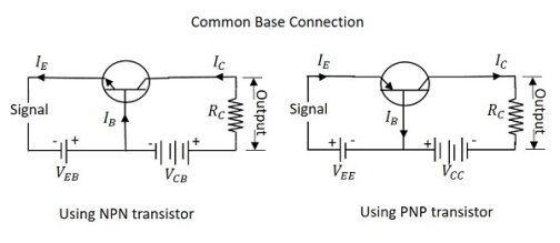
Figure 6. CB configuration
Let us consider the NPN transistor in the CB configuration. When the emitter voltage is applied, as it is forward biased, the electrons from the negative terminal repel the emitted electrons, and current flows through the emitter and base to the collector to contribute collector current.
The collector voltage VCB is kept constant. In CB configuration, the input current is the emitter current IE and the output current is the collector current IC.
Current Amplification Factor α
The ratio of change in collector current ΔIC to the change in emitter current ΔIE when collector voltage VCB is kept constant is called a Current amplification factor.
It is denoted by α.
α=ΔIC/ΔIE at constant VCB
The expression for Collector current
Along with the emitter current flowing, there is some amount of base current IB which flows through the base terminal due to electron-hole recombination. As the collector-base junction is reverse biased, there is another current that is flown due to minority charge carriers. This is the leakage current which can be understood as as Ileakage. This is due to minority charge carriers and hence small.
The emitter current that reaches the collector terminal is αIE
Total collector current
IC=αIE + Ileakage
If the emitter-base voltage VEB = 0 there flows a small leakage current, which can be termed as ICBO collector−base current with output open collector−base current with the output open.
The collector current therefore can be expressed as
IC=αIE+ICBO
IE=IC+IB
IC=α(IC+IB)+ICBO
IC(1−α)=αIB+ICBO
IC=(α1−α)IB+(ICBO1−α)
IC=(α1−α)IB+(11−α)ICBO
Hence the above derived is the expression for collector current. The value of collector current depends on base current and leakage current along with the current amplification factor of that transistor in use.
Feature of CB configuration :
- Common terminal: base
- Input current: IE
- O/p current IC
- I/P Vtg. : VEB
- O/P Vtg. VCB
- Current gain:
 ( less than 1)
 - Vtg. Gain: medium
- Input resistance: very low (20-)
- O/P resistance: very high (1 m-2)
Application: as a preamplifier
Common Emitter CE Configuration
The name itself implies that the Emitter terminal is taken as a common terminal for both input and output of the transistor. The common emitter connection for both NPN and PNP transistors is as shown in the following figure.
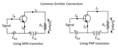
Figure 7. CE configuration
Just as in CB configuration, the emitter junction is forward- biased and the collector junction is the reverse- biased. The flow of electrons is controlled in the same manner.
The input current is the base current IB and the output current is the collector current IC here.
Base Current Amplification factor β
The ratio of change in collector current ΔIC to the change in base current ΔIB is known as Base Current Amplification Factor. It is denoted by β
β=ΔIC/ΔIB
The relation between β and α
The relation between the base current amplification factor and emitter current amplification factor.
β=ΔIC/ΔIB
α=ΔIC/ΔIE
IE=IB+IC
ΔIE=ΔIB+ΔIC
ΔIB=ΔIE−ΔIC
We can write
β=ΔIC/∆IE−ΔIC
β=ΔIC/ΔIE/ΔIE/ΔIE−ΔIC/ΔIE
α=ΔIC/ΔIE
We have
α=ΔIC/ΔIE
Therefore,
β=α(1−α)
From the above equation, it is evident that, as α approaches 1, β reaches infinity.
The expression for Collector Current
In the Common Emitter configuration, IB is the input current and IC is the output current.
We know
IE=IB+IC
And
IC=αIE+ICBO
=α(IB+IC)+ICBO
IC(1−α)=αIB+ICBO
IC=α1−αIB+11−αICBO
If the base circuit is open that is if IB = 0,
The collector-emitter current with a base open is ICEO
ICEO=11−αICBO
Substituting the value we get
IC=α1−αIB+ICEO
IC=βIB+ICEO
Hence the equation for collector current is obtained.
CE features:
Parameter | Characteristics |
Voltage gain | Medium |
Current gain | Medium |
Power gain | High |
Input/Output Relationship | 180 |
Input resistance | Medium |
Output resistance | Medium |
Common Collector Configuration
The name itself implies that the Collector terminal is taken as a common terminal for both input and output of the transistor. The common collector connection for both NPN and PNP transistors is as shown in the following figure.
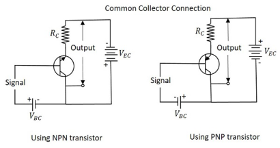
Figure 8. CC configuration
Just as in CB and CE configurations, the emitter junction is forward biased and the collector junction is reverse biased. The flow of electrons is controlled in the same manner. The input current is the base current IB and the output current is the emitter current IE here.
Current Amplification Factor γγ
The ratio of change in emitter current ΔIE to the change in base current ΔIB is known as the Current Amplification factor in common collector CC configuration. It is denoted by γ.
γ=ΔIE/ΔIB
- The current gain in CC configuration is the same as in CE configuration.
- The voltage gain in the CC configuration is always less than 1.
The relation between γ and α
Let us try to draw some relation between γ and α
γ=ΔIE/ΔIB
α=ΔIC/ΔIE
IE=IB+IC
ΔIE=ΔIB+ΔIC
ΔIB=ΔIE−ΔIC
Substituting the value of IB, we get
γ=ΔIE/ΔIE−ΔIC
Dividing by ΔIE/ΔIE
γ=ΔIE/ΔIE/ΔIE/ΔIE−ΔIC/ΔE
1/1−α
γ=1/1−α
The expression for collector current
We know
IC=αIE+ICBO
IE=IB+IC
=IB+(αIE+ICBO)
IE(1−α)=IB+ICBO
IE=IB1−α+ICBO1−α
IC≅IE=(β+1)IB+(β+1)ICBO
The above is the expression for collector current.
Features:
- This configuration provides a current gain but no voltage gain.
- In CC configuration, the input resistance is high and the output resistance is low.
- The voltage gain provided by this circuit is less than 1.
- The sum of collector current and base current equals emitter current.
Key Take-Away:
The common base circuit works best as a current buffer. It can take an input current at a low input impedance, and deliver nearly that same current to a higher impedance output.
The common emitter has low input impedance, high output impedance, high voltage gain, and high current gain
The common collector can be used for impedance matching between an amplifier stage with a high output impedance and an amplifier stage with a low input impedance.
The hybrid pi model of a BJT is a small signal model, named after the “p”-like equivalent circuit for a bipolar junction transistor. The model is shown in the figure. It consists of an input impedance, rp, an output impedance r0, and a voltage-controlled current source described by the transconductance, gm. Besides it contains the base-emitter capacitances, the junction capacitance, Cj, BE, and the diffusion capacitance, Cd, BE, and the base-collector junction capacitance, Cj, BC, also referred to as the Miller capacitance. |

Figure 9. A small signal hybrid model of BJT
The transconductance, gm, of a bipolar transistor is defined as the change in the collector current divided by the change of the base-emitter voltage.
Gm =  Ic /
Ic /  VBE = Ic/ nVt-----------------------------(1)
The base input resistance, rp, is defined as the change of the emitter-base voltage divided by the change of the base current.
 =
=  VBE/
VBE/  IB = β
  VBE/
VBE/ IC = β / gm = n Vt/ IB -------------------------(2)
The output resistance, ro, is defined as:
Ro =  VCE/
VCE/  Ic =
Ic =  VCB /
VCB /  IC = |VA|/ IC ------------------------------------(3)
The base-emitter and base-collector junction capacitances are given by:
Cj, BE = Cj, BEO/  1 – VBE/ɸi, BE----------------------------------------------(4)
Cj,BC = Cj,BC0/  1 – VBC/ ɸi, BC -----------------------------------------(5)
For the case where the base-emitter and base-collector junctions are abrupt. Since the base-emitter is strongly forward biased in the forward active mode of operation, one has to also include the diffusion capacitance of the base:
Cd, BE = IE/Vt τB ------------------------------------------------------------------(6)
Based on the small-signal model shown in Figure we can now calculate the small-signal current gain versus frequency, hfe, of a BJT biased in the forward active mode and connected in a common emitter configuration. The maximum current gain is calculated while shorting the output, resulting in:
Hfe = ic/ib = gm/ ib v = β/ 1+jw(Cj,BE + Cd,BE) rπ -----------------------------(7)
The unity gain frequency, fT, also called the transit frequency is obtained by setting the small-signal current gain, hfe, equals to one, resulting in:
|ic/ib| = 1= β/ 2π fT(Cj,BE + Cd,BE) rπ -----------------------------------------(8)
This transit frequency can be expressed as a function of the transit time, t:
fT = 1/ 2 π  -------------------------------------(9)
Where the transit time, t, equal:
τ = Cj,BE nVt/ IE + wB 2 / 2 Dn,B = τ E + τB ----------------------------(10)
The circuit model, therefore, includes the charging time of the base-emitter capacitance, tE, as well as the base transit time, tB, but not the transit time of the carriers through the base-collector depletion region, tC.
The collector transit time is
Rc = tc/2 = πd,BC/ 2 vsat ---------------------------------------------------(11)
The total transit time is given by
τ = Cj,BE nVt/ IE + wB 2 / 2 Dn,B + xd,BC/ 2 vsat = τ E + τB + τc ------------(12)
The maximum oscillation frequency, fMAX, is linked to the transit frequency, fT, and is obtained from:
Fmax = √ fT/ 2π RB Cj,BC-----------------------------------------(13)
Where RB is the total base resistance and Cj, BC is the base-collector capacitance.
Key take away:
- In the small-signal analysis, the transistor behaves as a voltage-controlled current source.
- The transistor operates in the linear region for the whole BJT with the small ac input signal
- If the input signal is too large. The fluctuations along the load line will drive the transistor into either saturation or cut-off.
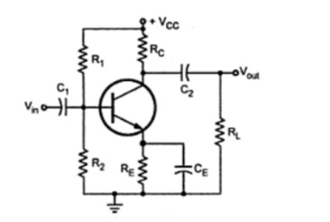
Figure 10. RC coupled CE Amplifier
The model consists of three RC networks that affect its gain as the frequency is reduces below midrange. These are,
· RC network formed by the input coupling capacitor C1 and the input impedance of the amplifier.
· RC network formed by the output coupling capacitor C2, resistance looking in at the collector, and load resistance.
· RC network formed by the emitter bypass capacitor CE and resistance looking in at the emitter.
Input RC network:
The following figure shows the input RC network formed by C1 and the input impedance of the amplifier.
The resistance value is Rin = R1 || R2 || Rin(base)
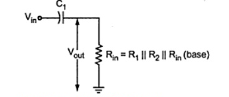
Figure 11: RC network
Applying voltage divider rule ,
Vout = (Rin /  Rin 2 + Xc1 2 ) Vin
A critical point in the amplifier response is generally accepted to occur when the output voltage is 70.7 % of the input. At critical point,
Rin /  Rin 2 + Xc1 2 = 0.707
At this condition, Rin = Xc1
Overall gain is reduced due to attenuation provided by the input RC network. The reduction in overall gain is given by,
Av = 20 log (Vout/Vin) = 20 log(0.707) =-3dB
The frequency fc at this condition is called lower critical frequency and it is given by,
Where fc = 1/ 2 π Rin C1
Where Rin = R1 || R2 || hie
Fc = 1/ 2π(R1||R2||hie) C1
If the resistance of input source is taken into account the above equation becomes,
Fc = 1/ 2π(Rs +Rin) C1
The phase angle in an input RC circuit is expressed as
 = tan -1 (XC1/Rin)
Output RC network:

Figure 12. Current source and current replaced by a voltage source
The above figure shows the output RC network formed by C2, resistance looking in at the collector, and load resistance.
The critical frequency for this RC network is given by,
Fc = 1/ 2π(Rc + RL) C2
The phase angle in output RC network is given as,
 = tan -1 (XC2/Rc + RL)
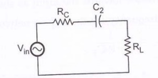
Figure13. Current source replaced by a voltage source
From the above figure,
(hie + RTH/β)
Is the resistance looking in at the emitter. It is derived as follows, R= (Vb / βIb) + hie / β
= Ib RTH / β Ib + hie/ β = Rth + hie/ β
Where RTH = R1 || R2 || Rs. It is the Thevenin's equivalent resistance looking from the base of the transistor towards the input.
The critical frequency for the bypass network is
Fc = 1/ 2π R CE
Or
Fc = 1/ 2π (hie + R TH/β) || RE] CE
Problem:
Determine the low-frequency response of the amplifier circuit shown in the figure.
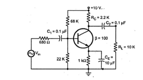
Solution:
It is necessary to analyze each network to determine the critical frequency of the amplifier.
a) Input RC network
Fc(input) = 1/ 2π[ Rs + (R1||R2||hie)] C1
= 1/ 2π[ 680 + (68K||22K||1.1K)] 0.1 x 10 -6
= 1/ 2π[ 680 + (1031.7)] 0.1 x 10 -6 = 929.8Hz
b) Output RC network
Fc(output) = 1/ 2π(Rc+RL) C2 = 1/2π(2.2K + 10 K) x 0.1 x 10 -6 = 130.45 Hz.
c) Bypass RC network
Fc(bypass) = 1/2π[(RTH+hie)/β] CE
RTH = R1||R2||R3 = 68K||22K||680= 653.28Ω
The above analysis shows that the input network produces the dominant lower critical frequency. Then the low-frequency response of the given amplifier is shown in the following figure.
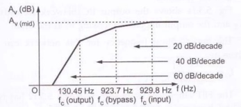
Figure 14.Low-frequency response
Key Take Away
- For high-frequency analysis or medium frequency analysis, large capacitors are replaced by a short circuit
As Xc = 1/wC
Because pf high value of capacitance even at the medium frequency where Xc  0.
0.
- For low-frequency analysis, we cannot consider Xc
 0 and the capacitor cannot be replaced by a short circuit. Hence we use 3 large capacitors CB, CE, CC.
Voltage gain:
In the small-signal equivalent circuit model. Remove RL and RS
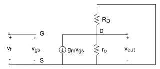
Figure 15.Small signal equivalent circuit model
Therefore, we get

Figure 16. Equivalent Small signal equivalent model
Vout = -gm vt (ro || RD)
Then unloaded voltage gain
Avo = vout / vt = -gm (ro||RD)
Input resistance
To calculate input resistance
Apply test voltage (or current) at the input and measure the test current or voltage.
Rin-Load amplifier with RL
Load amplifier with RL

Figure17 .Common source amplifier
It =0 - Rin = vt/it = ∞
Output resistance:
To calculate the output resistance
Rout -Load amplifier with RS
Measure the voltage or current at the output
Set the input source equal to zero.

Figure 18.CS Amplifier
Vgs =0 -- gm vgs =0 - vt = it(ro||RD)
Rout = vt/it = ro ||RD
Key Takeaways:
- These parameters are used to find the Q-point.
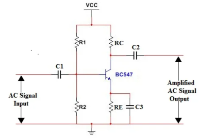
Figure 19.CE Amplifier
To design CE Amplifier:
Choose transistor
First, the transistor type should be chosen to meet the performance requirements
For example, if we use NPN transistor BC547 for greater amplification high β(Beta) Value must be chosen.
β is called amplification factor. With a high β value, the transistor can be turned ON with a low base current
Calculate Rc
To determine the current flow required to drive the following stage. By knowing the current flow required in the resistor, choose the collector voltage of around half the supply voltage to enable equal excursions of the signal up and down.
For Example
To find out collector resistor
Suppose the supply voltage and current as 15V and 1A. If 0.5A current is required at the output that is at the collector. The voltage needs to be half the supply voltage. So finally V=7.5V and I=0.5A(500mA).
Using Ohms law
V=IR
7.5=0.5xR
R=7.5/0.5
The collector resistor value is R=15Ω.
Calculate the emitter resistor
Usually, the voltage of around 1 volt or 10% of the supply voltage is chosen for the emitter voltage. This gives a good level of DC stability to the circuit.
For Example
To determine the emitter resistor
Suppose the supply voltage is 15V. So the emitter voltage should be 10% of the supply voltage. The emitter current should be the same as the collector current.
So finally V= 1.5V and I=0.5A.
Using Ohms Law V=IR
1.5=0.5xR
R=1.5/0.5
The emitter resistor is R=3Ω.
Determine base current:
To determine the base current divide the collector current by β
For Example
The collector current is 0.5A. The β value is 300.
Base current =Collector Current/β
Base Current=0.5/300
Base current=0.0016A
The Base current is 1.6mA.
Determine the base voltage
The base voltage is the sum of emitter voltage plus the base-emitter junction voltage. This is taken to be 0.6 volts for silicon and 0.2 volts for germanium transistors.
For Example
The emitter voltage is 1.5V. The transistor taken is a silicon transistor that has a 0.6V base-emitter junction voltage.
Base voltage= emitter voltage + 0.6
Base voltage= 1.5 + 0.6
Base voltage= 2.1V
Determine the base resistor
The voltage required at the base is 2.1V. It can be taken approximately as 2V.
Choose the ratio of R1 and R2 resistors to provide the voltage required at the base.
For choosing R1 and R2 resistor use the voltage divider formula.
Vout=(VsxR2/R1+R2)
For Example
The Resistor R1 and R2 are connected between 15V and GND.
Substitute the following value in the voltage divider formula. R1=1KΩ,R2=160Ω,Vs=15V.
Vout=(VsxR2/R1+R2)
Vout=(15x160/1000+160)
Vout=(2400/1160)
Vout=2V which the required voltage
Thus, we got 2V at the base using the voltage divider formula.
Emitter bypass capacitor
The gain of the circuit without a capacitor across the emitter resistor is approximately R3/R4. To increase the gain of AC signals, the emitter resistor bypass capacitor C3 is added. This should be calculated to have a reactance equal to R4 at the lowest frequency of operation. The formula to calculate bypass capacitor C3 is given below.
C=1/(2πf)Xc
For example
Xc is the emitter resistor(RE) value, that is 3Ω.
f is the frequency of the AC signal to be amplified. I am taking the frequency value as 95Mhz. That means I am going to amplify the AC signal that has a 95Mhz frequency.
Substitute the following values in C=1/(2πf)Xc formula.
π=3.14,Xc=3Ω,f=95Mhz,Mhz=10^6.
C=1/(2πf)Xc
C=1/(2x3.14x95x10^6x3)
C=5.587216x10^-10
C=558.72x10^-12
C=559x10^-12
Thus we can take approximately 600picofarad.
C=600pF.
Determine the value of the input capacitor value
The value of the input capacitor should equal the resistance of the input circuit at the lowest frequency to give a -3dB fall at this frequency. The total impedance of the circuit will be β times R3 plus any resistance external to the circuit, i.e. the source impedance. The external resistance is often ignored as this is likely not to affect the circuit unduly.
The formula for calculating the input capacitor value is
C=(1/2πfR)
Where
R is the resistance of the input circuit. The input circuit can be an oscillator or signal generator.
f is the frequency of the AC signal to be amplified.
For Example
Let us take the value of resistance of input circuit R=500Ω for example.
Substitute R=500Ω.and f=95Mhz in the formula C=(1/2πfR).
C=(1/2x3.14x95x10^6x500)
C=3.350x10^-12
C=3.3pF.
The practical method of finding the resistance of the input circuit for calculating the input capacitor is explained in STEP 5.
Determine the output capacitor value
Again, the output capacitor is generally chosen to equal the circuit resistance at the lowest frequency of operation. The circuit resistance is the emitter follower output resistance plus the resistance of the load, i.e. the circuit following.
For Example
To calculate the emitter follower resistance, turn the multimeter to resistance mode. Connect the positive probe to the collector terminal of the BC547 transistor and connect the negative probe to the ground where the emitter resistor is grounded.
Note down the resistance value using a multimeter. This is the method to find emitter follower resistance.
Let the resistance of the load be 1KΩ. Then the resistance to find output capacitor value is given below.
Resistance=Emitter follower resistance+Resistance of the circuit following.
After obtaining the resistance value apply the formula
C=1/2πfR
f is 95Mhz.
Key Take-Aways
Design procedure for CE amplifier and its parameters.
The lower cut-off frequency of multistage amplifier:
[1/ √ 1 + (fL/fL(n)) 2 ] n = 1/ √2
√2 = [1/ √ 1 + (fL/fL(n)) 2 ] n
Squaring both sides we get and taking nth root
2 1/n = 1 1 + (fL/fL(n) 2
2 1/n - 1 = 1 + (fL/fL(n) 2
Taking square root on both sides we get
√2 1/n – 1 = fL/fL(n)
FL(n) = fL/ √2 1/n – 1
Where fL(n) = lower 3db frequency of identical cascaded stages
FL = lower 3db frequency of single stage
n = number of stages
Key Take-Aways :
- Low-frequency analysis for CE amplifier its parameters and derivation
References:
- Fundamentals of Analog Circuits (English, Paperback, Floyd Thomas L.)
2. A Text Book on Analog Electronics - EE/E&T/IN by A Rajkumar, Made Easy Publications.
3. Analog Electronics by J.B Gupta
4. Design with Operational Amplifier and Analog Integrated Circuits by Sergio Franco.