Unit 4
Current Mirror
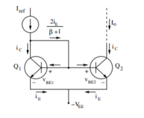
Figure 1. Current mirror
Consider the circuit shown with identical transistors, Q1 and Q2. Because both bases and emitters of the transistors are connected, KVL leads to vBE1 = vBE2. BJT operation is controlled by vBE. As vBE1 = vBE2 and transistors are identical, they should have similar iE, iB, and ic:
iB = iE/ β + 1 Io = ic = β iE/ β + 1
KCL = I ref = ic + 2 iE/ β + 1 = iE/ β + 1 + 2 iE/ β + 1= β + 2/ β + 1 . iE
Io/Iref = β / β + 2 = 1/ 1+2/β
For β >> 1, Io ≈ Iref (with an accuracy of 2/β). This circuit is called a “current mirror” as the two transistors work in tandem to ensure that current Io remains the same as Iref no matter what circuit is attached to the collector of Q2. As such, the circuit behaves as a current source and can be used to bias BJT circuits.
Variants
Current mirror with emitter resistors
One solution for variation of current over the compliance range is to introduce a small amount of resistance into the emitter of each transistor. These resistors are chosen to have a few tenths of a volt drop across them.
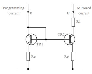
Figure 2. Current mirror transistor circuits with emitter resistors
For this circuit, both emitter resistors and transistors need to be matched. This is easy for the resistors where close tolerance resistors are easily available.
Wilson current mirror circuit
Another variation of the basic current mirror circuit is referred to as the Wilson mirror or Wilson current mirror.
Within the circuit, a third transistor is introduced. This transistor, shown as TR3 in the diagram keeps the collector of TR1 at a voltage equivalent to two diode drops below the rail voltage Vcc.
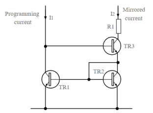
 Figure 3. Wilson current mirror transistor circuit
Current mirror circuits are useful, especially within integrated circuits. The components are incorporated into the design for little cost.
Key Take-Aways:
- Importance of the current mirror
- The variants in the current mirror
V-I characteristics
We know that for a BJT Ic = Ise Vbe/VT, ignoring the Early effect. Using this, and ignoring the base current) derive the following transcendental equation
IoutR1 = VT ln Iin Iout Is1 Is2
Consider the effect of the mirror and the multiple emitters of Q1.
In general, multiple emitter BJTs act as a single device, except that the emitter current is split evenly between the two emitters; basically, the base drive sets the total collector current, which is then split between both emitters.
Because we have n emitters in Q1, Is1 = nIs2. Then, using the fact that the mirror forces Iin = Iout, and we have the final result:
Iout = VT R2 lin
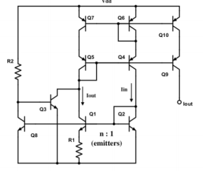
Figure 4.Self-biased current source
Output resistance
If VBC is greater than zero in output transistor Q2, the collector current in Q2 will be somewhat larger than for Q1 due to the Early effect.
In other words, the mirror has a finite output (or Norton) resistance given by the ro of the output transistor, namely:
RN = ro = VA + VCE / IC
Where VA is the Early voltage; and VCE, the collector-to-emitter voltage of the output transistor.
Minimum sustainable voltage:
To keep the output transistor active, VCB ≥ 0 V. That means the lowest output voltage that results in correct mirror behaviour, the compliance voltage, is VOUT = VCV = VBE under bias conditions with the output transistor at the output current level IC and with VCB = 0 V or, inverting the I-V relation above:
VCV = VT ln(IC/Is +1)
Where VT is the thermal voltage; and IS, the reverse saturation current or scale current.
Maximum usable load
This current source configuration, the figure also sometimes called a Peaking Current Source or gm-compensated mirror. Because the collector voltage VC of transistor Q1 is now more constant with changes in the input supply voltage as represented by VIN, it can be used as the base voltage of Q2 to produce a much more constant collector current in transistor Q2.
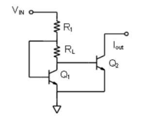
Figure 5. Peaking current source
Key TakeAways:
- V-I characteristics in the current mirror
- Definitions of Output resistance, Minimum sustainable voltage, maximum usable load
A differential amplifier is a device that is used to amplify the difference between the voltages applied at its inputs. Such circuits can be of two types viz.,
- Differential amplifiers built using transistors, either BJT or FET
- Differential amplifiers built using Op-Amps.
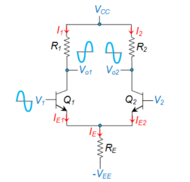
Figure 6. BJT Differential Amplifier
Here the input signals (V1 and V2) are applied to the base of the transistors while the output is collected across their collector terminals (Vo1 and Vo2).
- If V1 at Q1 is sinusoidal, then as V1 goes on increasing, the transistor starts to conduct and this results in a heavy collector current IC1 increasing the voltage drop across RC1, causing a decrease in Vo1.
- Due to the same effect, even IE1 increases which increases the common emitter current, IE resulting in an increase of voltage drop across RE.
- This means that the emitters of both transistors are driven towards positive which in turn implies that the base of Q2 would start to become more and more negative.
- This results in a decrease of collector current, IC2 which in-turn decreases the voltage drop across the collector resistor RC2, increasing the output voltage Vo2.
- This indicates that the changes in the sinusoidal signal observed at the input of transistor Q1 are reflected as such across the collector terminal of Q2 and appear with a phase difference of 180o across the collector terminal of Q1.
- The differential amplification can be driven by considering the output in-between the collector terminals of the transistors, Q1 and Q2.
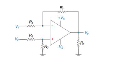
Figure 7. Differential Amplifier using Op-amp
Here V1 and V2 represent the voltages applied at its inverting and non-inverting input terminals and Ad refers to its differential gain.
The output of the differential amplifier is given as
Vo = Ad (V1 – V2) + Ac (V1 + V2/2)
where AC is called the common-mode gain of the amplifier.
Hence its output voltage will be equal to the sum of the output voltages produced by the Op-Amp circuit operating as an inverting amplifier and the Op-Amp circuit operating as a non-inverting amplifier.
Thus, one gets,
Vo = -Rf/R1 V1 + V2. Rf / R2 + R3 (1 + Rf/R1)
Now, if R1 = R2 and R3 = Rf, then
Vo = -Rf/R1 V1 + V2 . Rf/ R1 + Rf ( R1 + Rf/R1)
Vo = - Rf/R1 . V1 + V2 . Rf /R1
Vo = - Rf/R1 (V1 – V2)
This implies that the gain of the differential amplifier circuit is given by -Rf/R1.
Ad: differential gain
Ac: common-mode gain
Ad = V2-V1/2
Ac= V1+V2/2
CMRR = 20 log (|Ad|/|Ac|)
ICMR stands for Input common-mode reach.
It is the range of common input voltage supplied to the Differential Amplifier circuit for which all MOSFET would be in saturation mode.
Key Take-Aways:
- Differential amplifier working
- Derivation for Common mode and differential gain and CMRR
A differential amplifier is any two-input amplifier that has an output proportional to the difference of the inputs.
The defining equation for a differential amplifier is then:
Yo = A(xi1 -xi2) -------------------------------------(1)
Where the output yo and inputs xi could be either voltages or currents.
For the differential amplifier as shown in the figure the output expression is:
Yo = RB/RA(vi1 – vi2) -------------------------------------(2)
If the resistor values are chosen so that
RA/RB = RC/RD --------------------------------------------------------(3)
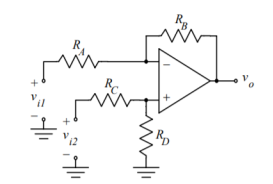
Figure 8. Differential amplifier
Ideally, this amplifier (or any differential amplifier) is sensitive only to the difference in the two input signals and is completely insensitive to any common component of the two signals. That is, if the difference in inputs remains constant, the output should not vary if the average value of the two inputs changes.
Vo = ADM (vi2-vi1) + ACM (vi2+vi1/2)
ADM – the amplification of the input signal difference vi2-vi1.
ACM – the amplification of the input signal average vi2+vi1/2
The quality of the differential amplifier is its ability to amplify the differential signal and suppress the common signal. A measure is the ratio of differential gain to the amplification of the average part of the input signals. The measure of quality is CMRR.
CMRR = 20 log Ad/Ac
AD= A2-A1/2
AC = A1+A2
Design a differential amplifier with the following performance requirements and restrictions:
A practical differential amplifier using uA741 opamp is shown below. With used components, the amplifier has a gain of around 5.
Av = -Rf/R1. Here Rf = 10K and R1 =2.2K, -Rf/R1 = -10/2.2 = -4.54 = ~-5.
A negative sign represents phase inversion. Use +/-12V DC dual supply for powering the circuit. UA 741 must be mounted on a hold
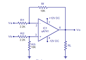
Figure 9. Practical differential amplifier
With the given specifications measure the individual input AC voltage gains at any frequency less than 1 kHz (set the other source to zero).
Compare results with theory
Calculate the common-mode and differential-mode gains and the CMRR from the experimental results.
Connect the two input nodes together and apply the AC signal of part B.
Measure the gain: this is a measurement of the common-mode gain. In order to measure the differential-mode gain, the inputs must be exact inverses: they will then have only differential components as their average will be zero.
Key Takeaways:
- Differential amplifier definition
- Design of differential amplifier
A circuit diagram of a differential amplifier using two op-amps is shown below. The main advantage of a differential amplifier with two op-amps is that it has increased overall gain. R1 is the input resistor for IC1 and R3 is the input resistor for IC2. Rf is the feedback resistor.
Va and Vb are the two input voltages and they are applied to the non-inverting inputs of IC2 and IC1 respectively. RL is the load resistor. V+ and V- are the positive and negative supply voltages.
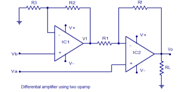
Figure10. Differential amplifier using op-amp
Derivation of voltage gain.
The equation for the output voltage V1 of the first op-amp is as follows:
V1 = (1+R2/R3) Vb---------------------------------------(1)
Here V1 and Va are the inputs for the second stage (IC2). The output voltage due to VA is
V0a = (1+Rf/R1) Va -----------------------------------(2)
Output voltage due to Vb is
Vob = (1+R2/R3) Vb (Rf/R1) ---------------------------------(3)
Overall output voltage Vo = Voa + Vob
Vo = - Rf/R1 (1+R2/R3)(Vb) + {(1+Rf/R1) Va)}-----------------------(4)
Let R1=R2 and Rf=R3 then we have
Vo = - Rf/R1 (1+R2/R3)(Vb) + {(1+Rf/R1) Va)}-----------------------(4)
Vo = - Rf/R1 (Rf+R1/Rf)/Rf (Vb) + {(R1+Rf/R1) Va)}-----------------------(5)
Vo = -(Rf+R1)/R1 Vb + (R1+Rf/R1) Va
Vo = (1+Rf/R1) (Va-Vb)
Therefore, overall voltage gain Av can be expressed using the equation
Av = Vo/(Va-Vb) = 1+(Rf/R1)
Compensation:
Optimal compensation of Op-Amps may be one of the most difficult parts of the design. A systematic approach results in near-optimal designs are introduced that apply to many other Op-Amps. The two most popular approaches are dominant-pole compensation and lead compensation.
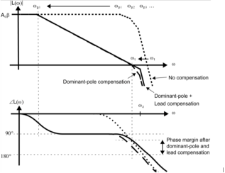
Figure 11. Compensation of op-amp
Key Take-Aways:
- Design of gain stages using op-amp
- Derivation for voltage gain
- Compensation of op-amp
References:
- Fundamentals of Analog Circuits (English, Paperback, Floyd Thomas L.)
2. A Text Book on Analog Electronics - EE/E&T/IN by A Rajkumar, Made Easy Publications.
3. Analog Electronics by J.B Gupta
4. Design with Operational Amplifier and Analog Integrated Circuits by Sergio Franco.