UNIT 4
Pulse and Delta Modulation
Here, the signal is transmitted in the form of pulses. It can be used to transmit analogue information. In pulse modulation, continuous signals are sampled at regular intervals.
Pulse modulation can be classified into two major types.
- Analogue: Indication of sample amplitude is infinitely variable
- Digital: Indicates sample amplitude at the nearest predetermined level.
Sampling is defined as, “The process of measuring the instantaneous values of continuous-time signal in a discrete form.”
Sample is a piece of data taken from the whole data which is continuous in the time domain.
When a source generates an analog signal and if that has to be digitized, having 1s and 0s i.e., High or Low, the signal has to be discretized in time. This discretization of analog signal is called as Sampling.
The following figure indicates a continuous-time signal x (t) and a sampled signal xs (t). When x (t) is multiplied by a periodic impulse train, the sampled signal xs (t) is obtained.
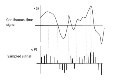
Fig.1: Sampled signal
Sampling Rate
To discretize the signals, the gap between the samples should be fixed. That gap can be termed as a sampling period Ts.
Sampling Frequency=1/Ts=fs
Where,
- Ts is the sampling time
- Fs is the sampling frequency or the sampling rate
Sampling frequency is the reciprocal of the sampling period. This sampling frequency, can be simply called as Sampling rate. The sampling rate denotes the number of samples taken per second, or for a finite set of values.
Nyquist Rate
Suppose that a signal is band-limited with no frequency components higher than W Hertz. That means, W is the highest frequency. For such a signal, for effective reproduction of the original signal, the sampling rate should be twice the highest frequency.
Which means,
fS=2W
Where,
- fS is the sampling rate
- W is the highest frequency
This rate of sampling is called as Nyquist rate.
Sampling Theorem
The sampling theorem, which is also called as Nyquist theorem, delivers the theory of sufficient sample rate in terms of bandwidth for the class of functions that are bandlimited.
The sampling theorem states that, “a signal can be exactly reproduced if it is sampled at the rate fs which is greater than twice the maximum frequency W.”
Let us consider a band-limited signal, i.e., a signal whose value is non-zero between some –W and W Hertz.
Such a signal is represented as x(f)=0 for ∣f∣>W
For the continuous-time signal x (t), the band-limited signal in frequency domain, can be represented as shown in the following figure.
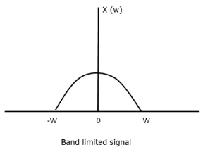
Fig.2: Band limited signal
If the signal x(t) is sampled above the Nyquist rate, the original signal can be recovered, and if it is sampled below the Nyquist rate, the signal cannot be recovered.
The following figure explains a signal, if sampled at a higher rate than 2w in the frequency domain.
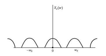
Fig.3: Sampled at a higher rate than 2w
The above figure shows the Fourier transform of a signal xs (t).
If fs<2W
The resultant pattern will look like the following figure.
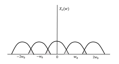
Fig.4: Resultant pattern
Here, the over-lapping of information is done, which leads to mixing up and loss of information. This unwanted phenomenon of over-lapping is called as Aliasing.
Aliasing
Aliasing can be referred to as “the phenomenon of a high-frequency component in the spectrum of a signal, taking on the identity of a low-frequency component in the spectrum of its sampled version.”
Key Takeaways:
- Sampling is defined as, “The process of measuring the instantaneous values of continuous-time signal in a discrete form.”
- The sampling theorem states that, “a signal can be exactly reproduced if it is sampled at the rate fs which is greater than twice the maximum frequency W.”
PAM
It is the simplest form of Pulse Modulation. In this type of modulation, each sample is made proportional to the amplitude of the signal at the instant of sampling. The PAM signal follows the amplitude of the original signal, as the signal traces out the path of the whole wave. Here a signal which is sampled at Nyquist rate can be reconstructed by passing it through an efficient Low Pass Filter (LPF) with exact cutoff frequency. It is very easy to generate and demodulate PAM. This technique transmits the data by encoding in the amplitude of a series of signal pulses.
There are two types of PAM.
- Single Polarity PAM: A fixed DC level is added to the signal so that the signal is always positive.
- Double Polarity PAM: Here the pulses are both positive and negative.
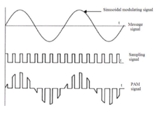
Fig. 5: PAM
PCM (Pulse Code Modulation)
- Pulse code modulation is a method that is used to convert an analog signal into a digital signal, so that modified analog signal can be transmitted through the digital communication network.
- PCM is in binary form, so there will be only two possible states high and low (0 and 1).
- The Pulse Code Modulation process is done in three steps Sampling, Quantization, and Coding.
- There are two specific types of pulse code modulations such as differential pulse code modulation (DPCM) and adaptive differential pulse code modulation (ADPCM)
Block Diagram
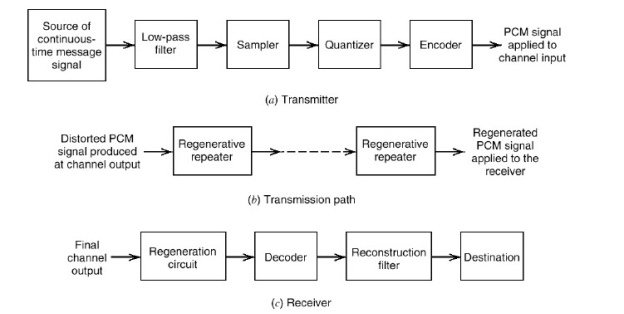
Fig. 6: PCM
To get the pulse code modulated waveform from an analog wave form at the transmitter end(source) of a communication circuit the amplitude of the analog signal samples at regular time intervals. The sampling rate or the number of samples per second is several times the maximum frequency.
The message signal is converted into binary form which is in the number of levels always to the power of 2. This process is called quantization.
At the receiver end, pulse code demodulator decodes the binary signal back into pulses with same quantum levels as those in the modulator.
Key Takeaways:
- In PAM, each sample is made proportional to the amplitude of the signal at the instant of sampling.
- Pulse code modulation is a method that is used to convert an analog signal into a digital signal, so that modified analog signal can be transmitted through the digital communication network.
DPCM Transmitter
The DPCM Transmitter consists of Quantizer and Predictor with two summer circuits.
Following is the block diagram of DPCM transmitter.
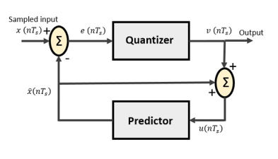
Fig. 7: DPCM
The signals at each point are named as −
- x(nTs) is the sampled input
- xˆ(nTs) is the predicted sample
- e(nTs) is the difference of sampled input and predicted output, often called as prediction error
- v(nTs) is the quantized output
- u(nTs) is the predictor input which is actually the summer output of the predictor output and the quantizer output
The predictor produces the assumed samples from the previous outputs of the transmitter circuit. The input to this predictor is the quantized versions of the input signal x(nTs).
Quantizer Output is represented as −
v(nTs)=Q[e(nTs)]
=e(nTs)+q(nTs)
Where q (nTs) is the quantization error
Predictor input is the sum of quantizer output and predictor output,
u(nTs)=xˆ(nTs)+v(nTs)
u(nTs)=xˆ(nTs)+e(nTs)+q(nTs)
u(nTs)=x(nTs)+q(nTs)
The same predictor circuit is used in the decoder to reconstruct the original input.
DPCM Receiver
The block diagram of DPCM Receiver consists of a decoder, a predictor, and a summer circuit. Following is the diagram of DPCM Receiver.
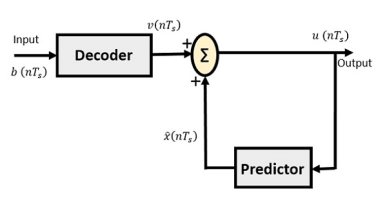
Fig. 7: DPCM Receiver
The notation of the signals is the same as the previous ones. In the absence of noise, the encoded receiver input will be the same as the encoded transmitter output.
As mentioned before, the predictor assumes a value, based on the previous outputs. The input given to the decoder is processed and that output is summed up with the output of the predictor, to obtain a better output.
Key Takeaways:
- The DPCM Transmitter consists of Quantizer and Predictor with two summer circuits.
- In the absence of noise, the encoded receiver input will be the same as the encoded transmitter output.
The type of modulation, where the sampling rate is much higher and in which the step size after quantization is of a smaller value Δ, such a modulation is termed as delta modulation.
Features
- The quality is moderate.
- The design of the modulator and the demodulator is simple.
- The stair-case approximation of output waveform.
- The step-size is very small, i.e., Δ deltadelta.
- The bit rate can be decided by the user.
- This involves simpler implementation.
Delta Modulation is a simplified form of DPCM technique, also viewed as 1-bit DPCM scheme. As the sampling interval is reduced, the signal correlation will be higher.
Delta Modulator
The Delta Modulator comprises of a 1-bit quantizer and a delay circuit along with two summer circuits. Following is the block diagram of a delta modulator.
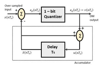
Fig. 8: Delta modulation
The predictor circuit in DPCM is replaced by a simple delay circuit in DM.
From the above diagram, we have the notations as −
- x(nTs)= over sampled input
- Ep(nTs) = summer output and quantizer input
- Eq(nTs) = quantizer output = v(nTs)
- xˆ(nTs) = output of delay circuit
- u(nTs) = input of delay circuit
Using these notations, now we shall try to figure out the process of delta modulation.
Ep(nTs)=x(nTs)−xˆ(nTs) ---------equation 1
=x(nTs)−u([n−1]Ts
=x(nTs)−[xˆ[[n−1]Ts]+v[[n−1]Ts]] -------equation 2
Further,
v(nTs)=eq(nTs)=S.sig.[ep(nTs)] ---------equation 3
u(nTs)=xˆ(nTs)+eq(nTs)
Where,
- xˆ(nTs) = the previous value of the delay circuit
- Eq(nTs) = quantizer output = v(nTs)
Hence,
u(nTs)=u([n−1]Ts)+v(nTs) ---------equation 4
Which means,
The present input of the delay unit
= The previous output of the delay unit + the present quantizer output the present quantizer output
Assuming zero condition of Accumulation,

Accumulated version of DM output =  --------equation 5
Now, note that
xˆ(nTs)=u([n−1]Ts)
= ---------equation 6
Delay unit output is an Accumulator output lagging by one sample.
From equations 5 & 6, we get a possible structure for the demodulator.
A Stair-case approximated waveform will be the output of the delta modulator with the step-size as delta (Δ). The output quality of the waveform is moderate.
Delta Demodulator
The delta demodulator comprises of a low pass filter, a summer, and a delay circuit. The predictor circuit is eliminated here and hence no assumed input is given to the demodulator.
Following is the diagram for delta demodulator.
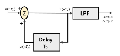
Fig. 9: Delta demodulator
From the above diagram, we have the notations as −
- vˆ(nTs) is the input sample
- uˆ(nTs) is the summer output
- x¯(nTs) is the delayed output
A binary sequence will be given as an input to the demodulator. The stair-case approximated output is given to the LPF.
Low pass filter is used for many reasons, but the prominent reason is noise elimination for out-of-band signals. The step-size error that may occur at the transmitter is called granular noise, which is eliminated here. If there is no noise present, then the modulator output equals the demodulator input.
Advantages of DM Over DPCM
- 1-bit quantizer
- Very easy design of the modulator and the demodulator
However, there exists some noise in DM.
- Slope Over load distortion (when Δ is small)
- Granular noise (when Δ is large)
The reconstructed message becomes contaminated with decoding + quantization noise.
The PCM signal will get contaminated by random noise ⇒causes bit errors in the message ⇒decoding noise.

Decoding noise power

Multiplexing is the process of combining multiple signals into one signal, over a shared medium.
- The process is called as analog multiplexing if these signals are analog in nature.
- If digital signals are multiplexed, it is called as digital multiplexing.
Multiplexing was first developed in telephony. A number of signals were combined to send through a single cable. The process of multiplexing divides a communication channel into several number of logical channels, allotting each one for a different message signal or a data stream to be transferred. The device that does multiplexing, can be called as a MUX.
The reverse process, i.e., extracting the number of channels from one, which is done at the receiver is called as demultiplexing. The device which does demultiplexing is called as DEMUX.
The following figures illustrates the concept of MUX and DEMUX. Their primary use is in the field of communications.
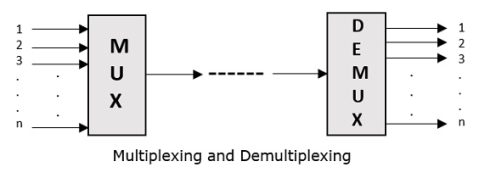
Fig.10: MUX and DEMUX
Types of Multiplexers
There are mainly two types of multiplexers, namely analog and digital. They are further divided into FDM, WDM, and TDM. The following figure gives a detailed idea about this classification.
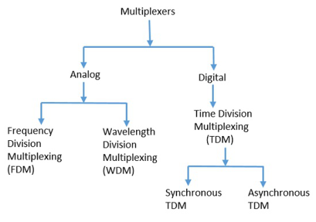
There are many types of multiplexing techniques. Of them all, we have the main types with general classification, mentioned in the above figure. Let us take a look at them individually.
Analog Multiplexing
The analog multiplexing techniques involve signals which are analog in nature. The analog signals are multiplexed according to their frequency (FDM) or wavelength (WDM).
Frequency Division Multiplexing
In analog multiplexing, the most used technique is Frequency Division Multiplexing (FDM). This technique uses various frequencies to combine streams of data, for sending them on a communication medium, as a single signal.
Example − A traditional television transmitter, which sends a number of channels through a single cable uses FDM.
Wavelength Division Multiplexing
Wavelength Division multiplexing (WDM) is an analog technique, in which many data streams of different wavelengths are transmitted in the light spectrum. If the wavelength increases, the frequency of the signal decreases. A prism which can turn different wavelengths into a single line, can be used at the output of MUX and input of DEMUX.
Example − Optical fiber Communications use the WDM technique, to merge different wavelengths into a single light for the communication.
Digital Multiplexing
The term digital represents the discrete bits of information. Hence, the available data is in the form of frames or packets, which are discrete.
Time Division Multiplexing (TDM)
In TDM, the time frame is divided into slots. This technique is used to transmit a signal over a single communication channel, by allotting one slot for each message.
Of all the types of TDM, the main ones are Synchronous and Asynchronous TDM.
Synchronous TDM
In Synchronous TDM, the input is connected to a frame. If there are ‘n’ number of connections, then the frame is divided into ‘n’ time slots. One slot is allocated for each input line.
In this technique, the sampling rate is common for all signals and hence the same clock input is given. The MUX allocates the same slot to each device at all times.
Asynchronous TDM
In Asynchronous TDM, the sampling rate is different for each of the signals and a common clock is not required. If the allotted device, for a time slot transmits nothing and sits idle, then that slot is allotted to another device, unlike synchronous.
This type of TDM is used in Asynchronous transfer mode networks.
Demultiplexer
Demultiplexers are used to connect a single source to multiple destinations. This process is the reverse of multiplexing. As mentioned previously, it is used mostly at the receivers. DEMUX has many applications. It is used in receivers in the communication systems. It is used in arithmetic and logical unit in computers to supply power and to pass on communication, etc.
Demultiplexers are used as serial to parallel converters. The serial data is given as input to DEMUX at regular interval and a counter is attached to it to control the output of the demultiplexer.
Data Multiplexer
In digital electronics, multiplexers are also known as data selectors because they can “select” each input line, are constructed from individual Analogue Switches encased in a single IC package as opposed to the “mechanical” type selectors such as normal conventional switches and relays.
They are used as one method of reducing the number of logic gates required in a circuit design or when a single data line or data bus is required to carry two or more different digital signals. For example, a single 8-channel multiplexer.
Generally, the selection of each input line in a multiplexer is controlled by an additional set of inputs called control lines and according to the binary condition of these control inputs, either “HIGH” or “LOW” the appropriate data input is connected directly to the output. Normally, a multiplexer has an even number of 2n data input lines and a number of “control” inputs that correspond with the number of data inputs.
Note that multiplexers are different in operation to Encoders. Encoders are able to switch an n-bit input pattern to multiple output lines that represent the binary coded (BCD) output equivalent of the active input.
We can build a simple 2-line to 1-line (2-to-1) multiplexer from basic logic NAND gates as shown.
2-input Multiplexer Design
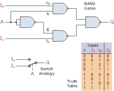
Fig.11:2-input Multiplexer Design
References:
1. Haykin S., "Communications Systems," John Wiley and Sons, 2001.
2. Proakis J. G. And Salehi M., "Communication Systems Engineering," Pearson Education,
2002.
3. Taub H. And Schilling D.L., "Principles of Communication Systems,” Tata McGraw Hill,
2001.
4. Wozencraft J. M. And Jacobs I. M., “Principles of Communication Engineering,” John
Wiley, 1965.
5. Barry J. R., Lee E. A. And Messerschmitt D. G., “Digital Communication,” Kluwer
Academic Publishers, 2004.
6. Proakis J.G., “Digital Communications',' 4th Edition, McGraw Hill, 2000.
7. Abhay Gandhi, “Analog and Digital Communication,” Cengage publication, 2015.