Unit – 2
Basic Programming concepts
Symbol | Symbol Name | Purpose |
 | Start/Stop | Used at the beginning and end of the algorithm to show start and end of the program. |
 | Process | Indicates processes like mathematical operations. |
 | Input/ Output | Used for denoting program inputs and outputs. |
 | Decision | Stands for decision statements in a program, where answer is usually Yes or No. |
 | Arrow | Shows relationships between different shapes. |
 | On-page Connector | Connects two or more parts of a flowchart, which are on the same page. |
 | Off-page Connector | Connects two parts of a flowchart which are spread over different pages. |
Data Transfer Instruction
These instructions transfer data between registers or between memory and registers. The instruction is used to copy data from source to destination while copying the contents of source cannot be modified.
OPCODE | OPERAND | DESCRIPTION |
MOV | Rd, Rs Rd, M M, Rs | Transfer the content of the source to the destination |
MVI | Rd, Data M, data | Move immediate data into the destination register |
LXI | Reg. Pair, data | Mov 16-bit data into the register pair |
LDA | 16 bit address | Load accumulator with data present at the specified address |
XCHG | - | Exchange the contents of HL with DE |
For example MOV B, C
MVI B,20H
LXI H, 4020H
LDA 6000H
Arithmetic Instructions
- Addition
- Subtraction
- Increment
- Decrement
OPCODE | OPERAND | DESCRIPTION |
ADD | R M | Add the contents of register with the contents of accumulator and save in accumulator |
ADC | R M | Add the contents of register with the contents of accumulator with carry and save in accumulator |
ADI | 8 bit data | Add data with the contents of accumulator |
DAD | Reg pair | Add register pair to H-L pair |
SUB | R M | Subtract the contents of the reg from the contents of the accumulator and save in accumulator |
SBB | R M | Subtract the contents of the reg with borrow from the contents of the accumulator and save in accumulator |
SUI | 8 bit data | Subtract data with contents of accumulator |
INR | R M | Increment register or memory by one |
DCR | R M | Decrement register or memory by one |
For example:
ADD C
ADC M
ADI 40H
DAD HL
SUB B
SUI 20H
INR C
The logical operations are:
- AND
- OR
- XOR
- Rotate
- Compare
- Complement
OPCODE | OPERAND | DESCRIPTION |
CMP | R M | Compare the contents of register or memory with accumulator |
ANA | R M | Logical add the contents of register with accumulator |
ANI | 8 bit data | Logical and the data with accumulator |
XRA | Reg pair | Add register pair to H-L pair |
ORA | R M | XOR the contents of the register with accumulator |
RLC | - | Rotate accumulator left |
RRC | - | Rotate accumulator right |
CMA | - | Complement accumulator |
For example
CMP C
ANA B
ANI 40H
XRA M
ORA C
RLC
Branching Instructions
These instructions alter the normal sequential flow conditionally or unconditionally
OPCODE | OPERAND | DESCRIPTION |
JMP | 16-bit address | Jump unconditionally to the given location |
JC | 16-bit address | Jump if carry |
JNC | 16-bit address | Jump if no carry |
JZ | 16-bit address | Jump if zero |
JNZ | 16-bit address | Jump if no zero |
CALL | 16-bit address | Call unconditionaly |
RET | 16-bit address | Return unconditionally |
RST | 16-bit address | Restart (Software Interrupts) |
For example
JMP 2000H
RET
RST 6
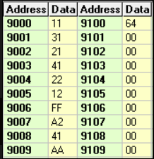
Let us suppose that 10 data are stored in memory location from 9000H to 9009H. These data are to be added and let us store the result in memory location 9100H.
Algorithm:
Start.
- Load into register pair HL from memory location 9000H.
- Load into register pair DE from memory location 9100H.
- Move 09 into register C as counter.
- Move the content of memory M into accumulator A.
- Increment register pair HL by 1.
- Add content of memory M with the contents of the accumulator A.
- Decrement value of register C by 1.
- If no zero is present, go to step 6 else go to step 10.
- Store the content of accumulator A into memory location pointed by register pair DE.
- Terminate the program.
Program Code:
LXI H, 9000H
LXI D, 9100H
MVI C, 09H
MVI B, 00H
MOV A, M
UP:
INX H
ADD M
JNC DOWN
INR B
DOWN:
DCR C
JNZ UP
STAX D
MOV A, B
STA 9101H
HLT
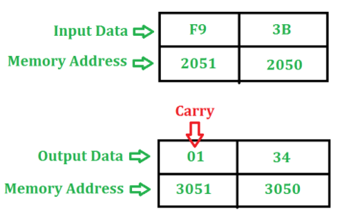
Write an assembly language program to add two 8-bit numbers stored at address 2050 and address 2051 in 8085 microprocessor. The starting address of the program is taken as 2000.
- Load the first number from memory location 2050 to accumulator.
- Move the content of accumulator to register H.
- Load the second number from memory location 2051 to accumulator.
- Then add the content of register H and accumulator using “ADD” instruction and storing result at 3050
- The carry generated is recovered using “ADC” command and is stored at memory location 3051
Program –
Memory Address | Mnemonics | Comment |
2000 | LDA 2050 | A<- [2050] |
2003 | MOV H, A | H<-A |
2004 | LDA 2051 | A<- [2051] |
2007 | ADD H | A<-A+H |
2008 | MOV L, A | L←A |
2009 | MVI A 00 | A←00 |
200B | ADC A | A←A+A+carry |
200C | MOV H, A | H←A |
200D | SHLD 3050 | H→3051, L→3050 |
2010 | HLT |
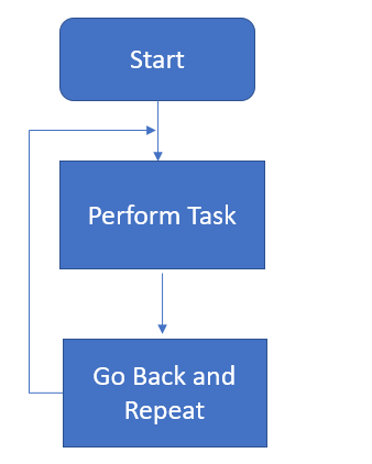
Continuous loop-repeat task continuously
Conditional loop-repeats a task until certain data conditions are met.
Flowchart of continuous loop
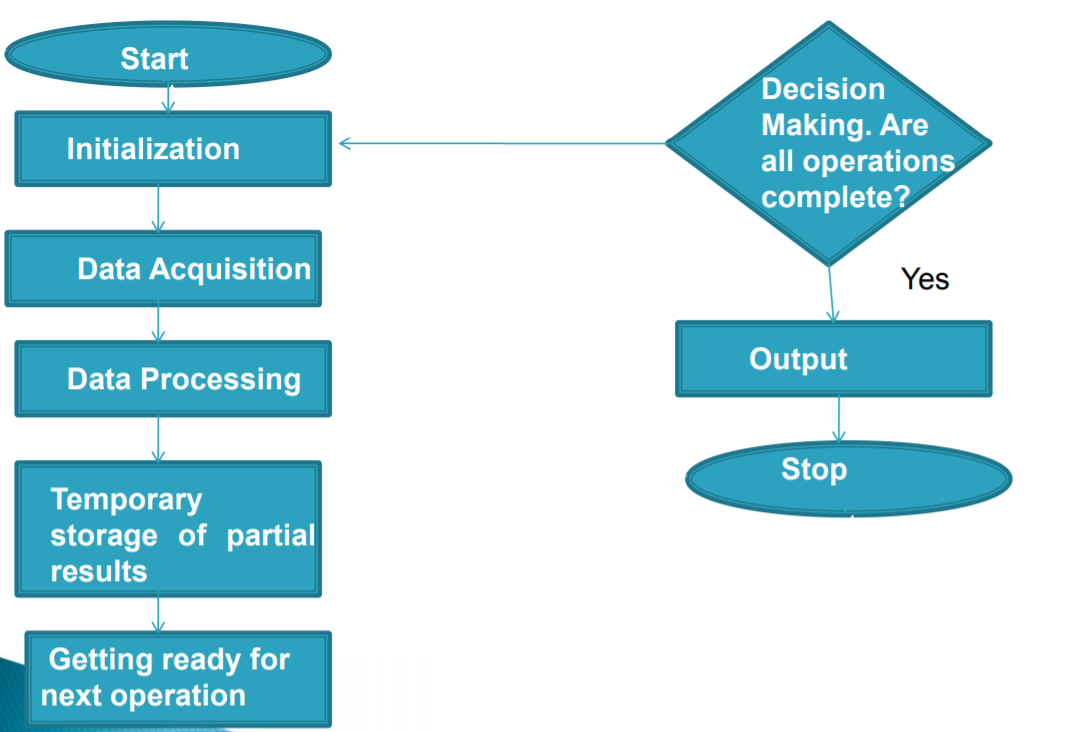
Looping-In this technique, the program is instructed to execute certain set of instructions repeatedly to execute a particular task number of times.
Counting-This technique allows programmer to count how many times the instruction/set of instructions are executed.
Indexing-This technique allows programmer to point or refer the data stored in sequential memory location one by one.
Load register pair immediate
• LXI Reg. Pair, 16-bit data.
• The instruction loads 16-bit data in the register pair designated in the operand.
• Example: LXI H, 2034H or LXI H, XYZ
Load H and L registers direct LHLD 16-bit address
The instruction copies the contents of the memory location pointed out by the 16-bit address into register L and copies the contents of the next memory location into register H. The contents of source memory locations are not altered.
Example: LHLD 2040H
MOV R, M
R, M copies data byte from Memory to Register. Memory location, its location is specified by the contents of the HL registers.
Example: MOV B, M
Load accumulator indirect
DATA TRANSFER FROM MEMORY TO MICROPROCESSOR
LDAX B/D Reg. Pair
The contents of the designated register pair point to a memory location. This instruction copies the contents of that memory location into the accumulator. The contents of either the register pair or the memory location are not altered.
Example: LDAX B Load accumulator
LDA 16-bit address. The contents of a memory location, specified by a 16-bit address in the operand, are copied to the accumulator.
The contents of the source are not altered.
Example: LDA 2034H
MOV M, R
This instruction copies the contents of the source.
The source register is not altered.
As one of the operands is a memory location, its location is specified by the contents of the HL registers.
Example: MOV M, B STA 16-bit address
The contents of the accumulator are copied into the memory location specified by the operand. This is a 3-byte instruction, the second byte specifies the low-order address and the third byte specifies the high-order address.
Example: STA 4350H
STAX Reg. Pair: The contents of the accumulator are copied into the memory location specified by the contents of the operand (register pair).
The contents of the accumulator are not altered.
Example: STAX B
Increment register pair by 1 INX R The contents of the designated register pair are incremented by 1 and the result is stored in the same place.
Example: INX H Decrement register pair by 1 DCX R The contents of the designated register pair are decremented by 1 and the result is stored in the same place.
Example: DCX H
Add memory
ADD M: The contents of the operand (memory) are added to the contents of the accumulator and the result is stored in the accumulator.
The operand is a memory location, its location is specified by the contents of the HL registers.
All flags are modified to reflect the result of the addition.
Subtract memory
SUB M: The contents of the operand (memory) are subtracted to the contents of the accumulator and the result is stored in the accumulator. The operand is a memory location, its location is specified by the contents of the HL registers. All flags are modified to reflect the result of the Subtraction. Increment memory by 1/Decrement memory by 1
INR M/DCR M: The contents of the memory are incremented by 1 using INR and decremented by 1 using DCR and the result is stored in the same place. The operand is a memory location, its location is specified by the contents of the HL registers.
Store H and L registers indirect SHLD 16-bit address. The contents of register L are stored into the memory location specified by the 16- bit address in the operand and the contents of H register are stored into the next memory location by incrementing the operand. The contents of registers HL are not altered. This is a 3-byte instruction, the second byte specifies the low-order address and the third byte specifies the high-order address. Example: SHLD 2470H
Compare (register or memory) with accumulator (CMP R/M) –
This is a 1-byte instruction. It compares the data byte in the register or memory with the contents of accumulator.
- If A less than (R/M), the CY flag is set and zero flag is reset.
- If A equals to (R/M), the Zero flag is set and CY flag is reset.
- If A greater than (R/M), the CY and Zero flag are reset.
When memory is an operand, its address is specified by HL Pair. No contents are modified; however, all remaining flags (S, P, AC) are affected according to the result of subtraction.
Example:
Let register B contains data byte 62H and the accumulator A contains 57H. Then,
Instruction- CMP B
Before execution: A = 57, B = 62
After execution: A = 57, B = 62
Flags: As A less than B, thus CY is set and Z flag is reset.
CY=1, Z=0
Compare immediate with accumulator (CPI 8-bit) –
This is a 2-byte instruction, the second byte being 8-bit data. It compares the second byte with the contents of accumulator.
If A less than 8-bit data, the CY flag is set and zero flag is reset.
If A equals to 8-bit data, the Zero flag is set and CY flag is reset.
If A greater than 8-bit data, the CY and Zero flag are reset.
No contents are modified; however, all remaining flags (S, P, AC) are affected according to the result of subtraction.
Example:
Let the accumulator A contains C2H. Then,
Instruction- CPI C2H
Before execution: A = C2, B = C2
After execution: A = C2, B = C2
Flags: As A equals to the data byte, thus Z is set and CY flag is reset.
CY=0, Z=1
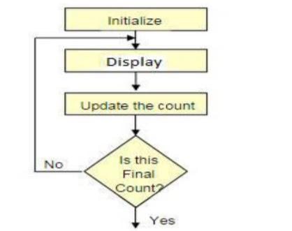
A counter is designed simply by loading appropriate number into one of the registers and using INR or DNR instructions.
• Loop is established to update the count.
• Each count is checked to determine whether it has reached final number; if not, the loop is repeated.
Time Delay:
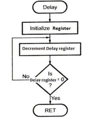
Procedure used to design a specific delay.
A register is loaded with a number, depending on the time delay required and then the register is decremented until it reaches zero by setting up a loop with conditional jump instruction.
LOOP: MVI C, FFH; Load register C 7
DCR C; Decrement C 4
JNZ LOOP; Jump back to 10/7 decrement C
Clock frequency of the system = 2 MHz Clock period= 1/T= 0.5 μs
Time to execute MVI = 7 T states * 0.5= 3.5 μs
Time Delay in Loop TL= T*Loop T states * N10 = 0.5 * 14* 255 = 1785 μs = 1.8 ms
N10 = Equivalent decimal number of hexadecimal count loaded in the delay register
TLA= Time to execute loop instructions =TL – (3T states* clock period) =1785-1.5=1783.5 μs L
The 8085 has five hardware interrupts
(1) TRAP
(2) RST 7.5
(3) RST 6.5
(4) RST 5.5
(5) INTR
TRAP: This interrupt is a non-maskable interrupt. It is unaffected by any mask or interrupt enable. TRAP has the highest priority and vectored interrupt. TRAP interrupt is edge and level triggered. This means that the TRAP must go high and remain high until it is acknowledged. In sudden power failure, it executes a ISR and send the data from main memory to backup memory. The signal, which overrides the TRAP, is HOLD signal. (i.e., If the processor receives HOLD and TRAP at the same time then HOLD is recognized first and then TRAP is recognized).
There are two ways to clear TRAP interrupt.
1. By resetting microprocessor (External signal)
2. By giving a high TRAP ACKNOWLEDGE (Internal signal)
RST 7.5: The RST 7.5 interrupt is a maskable interrupt. It has the second highest priority. It is edge sensitive. i.e., Input goes to high and no need to maintain high state until it recognized. Maskable interrupt. It is disabled by,
1. DI instruction
2. System or processor reset.
3. After reorganization of interrupt.
Enabled by EI instruction.
RST 6.5 and 5.5: The RST 6.5 and RST 5.5 both are level triggered. i.e., Inputs goes to high and stay high until it recognized.
Maskable interrupt. It is disabled by,
1.DI, SIM instruction
2.System or processor reset.
3. After reorganization of interrupt. Enabled by EI instruction. The RST 6.5 has the third priority whereas RST 5.5 has the fourth priority.
INTR: INTR is a maskable interrupt. It is disabled by,
1.DI, SIM instruction
2.System or processor reset.
3.After reorganization of interrupt.
Enabled by EI instruction. Non- vectored interrupt. After receiving INTA (active low) signal, it has to supply the address of ISR. It has lowest priority. It is a level sensitive interrupt. i.e., Input goes to high and it is necessary to maintain high state until it recognized.
The following sequence of events occurs when INTR signal goes high.
1. The 8085 checks the status of INTR signal during execution of each instruction.
2. If INTR signal is high, then 8085 complete its current instruction and sends active low interrupt acknowledge signal, if the interrupt is enabled.
3. In response to the acknowledge signal, external logic places an instruction OPCODE on the data bus. In the case of multibyte instruction, additional interrupt acknowledge machine cycles are generated by the 8085 to transfer the additional bytes into the microprocessor.
4. On receiving the instruction, the 8085 save the address of next instruction on stack and execute received instruction.
References:
1. Microprocessor Architecture, Programming, and ...Book by Ramesh S. Gaonkar
2. 8085 Microprocessor: Programming and Interfacing Book by N. K. Srinath
3. 8085 Microprocessors & Its Application Book by Nagoorkani