UNIT 6
NANOTECHNOLOGY
Origin of Nanotechnology
While the word Nanotechnology is relatively new, the existence of nanostructures, and Nanodevices is not new. Such structures existed on the earth as life itself began though it is not known when humans use nanosized materials the first known, Roman glassmakers were fabricated glasses containing nanosized metals. When the material size of the object is reduced to the nanoscale, then it exhibits different properties than the same material in bulk form.
The concept, and idea of nanotechnology were originally discussed first time in 1959 by Richard Feynman, a renowned physicist. Richard Feynman in his talk “There's Plenty of Room at the Bottom,” described the feasibility of synthesis via direct manipulation of atoms. However, in 1974, the term "Nano-technology" was first used by Norio Taniguchi.
Nanoscience
Nanoscience deals with the study of properties of materials at nanoscales where properties differ significantly from those at a larger scale.
Nanotechnology
Nanotechnology deals with the design, characterization, production, and applications of nanostructures, and nanodevices, and nanosystems.
CHARACTERIZATION
Physical properties
Thermal properties: Nanomaterials are different from those of bulk materials. The Debye Temperature and ferroelectric phase transition temperature are lower for nanomaterials. The melting point of the nanogold decreases from 1200 K to 800K as the size of the particle decreases from 300 Å to 200 Å.
Optical properties: Different sized nanoparticles scatter different light incident on it, and hence they appear in different colours. For example, nanogold does not act as bulk gold. The nanoparticles of gold appear as orange, purple, red, or greenish depending on their grain size. The bulk copper is opaque whereas nanoparticle copper is transparent.
Magnetic properties: The magnetic properties of nanomaterials are different from that of bulk materials. In explaining the magnetic behaviour of nanomaterials, we use single domains unlike a large number of domains in bulk materials. The coercivity value of the single domain is very large.
For example, Fe, Co, and Ni are ferromagnetic in bulk but they exhibit super par magnetism. Na, K, and Rh are paramagnetic in bulk but they exhibit ferromagnetic. Cr is anti-ferromagnetic in bulk but they exhibit superparamagnetic.
Mechanical properties: The mechanical properties such as hardness, toughness, elastic modulus, young’s modulus, etc., of nanomaterials are different from that of bulk materials. In metals and alloys, the hardness, and toughness are increased by reducing the size of the nanoparticles. In ceramics, ductility, and superplasticity are increased by reducing the grain size. Hardness increases 4 to 6 times as one goes from bulk Cu to nanocrystalline, and it is 7 to 8 times for Ni.
Chemical properties
Nanocrystalline materials are strong, hard, erosion, and corrosion-resistant. They are chemically active and have the following chemical properties.
- In electrochemical reactions, the rate of increase in mass transport increases as the particle size decreases.
- The equilibrium vapour pressure, chemical potentials, and solubilities of nanoparticles are greater than that for the same bulk material.
- Most of the metals do not absorb hydrogen. But the hydrogen absorption increases with the decrease of cluster size in Ni, Pt, and Pd metals.
Basic principles of nanomaterials
- Increase in surface area to volume ratio
- Quantum confinement effect
Increase in surface area to volume ratio: The ratio of surface area to volume ratio is large for nanomaterials.
Example 1: To understand this let us consider a spherical material of radius ‘r’. Then its surface area to volume ratio is 3/r. Due to the decrease of r, the ratio increases predominantly.
Example 2: For one cubic volume, the surface ratio is 6m2. When it is divided into eight cubes its surface area becomes 12m2. When it is divided into 27 cubes its surface area becomes 18m2. Thus, when the given volume is divided into smaller pieces the surface area increases.
|
Figure 1: Surface area to volume ratio
Quantum confinement effect: According to band theory, the solid atoms have energy bands, and isolated atoms possess discrete energy levels. Nanomaterials are the intermediate state of solids and atoms. When the material size is reduced to the nanoscale, the energy levels of electrons change. This effect is called a quantum confinement effect. This affects the optical, electrical, and magnetic properties of nanomaterials.
Nanomaterials
All materials are composed of grains. The visibility of grains depends on their size. Convectional materials have grains varying in size from hundreds of microns to millimeters. The materials processing grains size ranging from 1 to 100 nm, known as Nanomaterials. Nanomaterials can be produced in different dimensionalities.
- One dimensional nanomaterial: Surface coatings, and thin films
- Two-dimensional nanomaterials: nanotubes nanowires, biopolymers
- Three-dimensional nanomaterials: nanoparticles, precipitates, colloids, quantum dots, nanocrystalline materials, fullerenes, or carbon nano-60.
Classification of nanostructured materials
In the past two decades, hundreds of novel NSMs (nanostructured materials) have been obtained therefore, the need for their classification becomes important.
NSMs as a subject of nanotechnology are low dimensional materials comprising of building units of a submicron or nanoscale size at least in one direction, and exhibiting size effects.
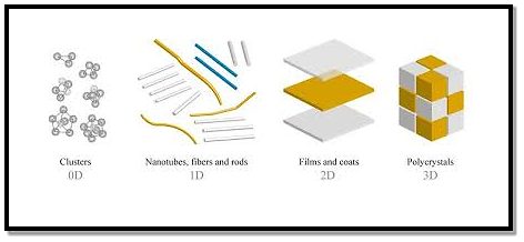
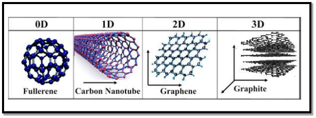
The first classification idea of NSMs was given by Gleiter in 1995, and further was explained by Skorokhod in 2000. However, Gleiter and Skorokhod scheme was not fully considered because 0D, 1D, 2D, and 3D structures such as fullerenes, nanotubes, and nanoflowers were not taken into account.
After that, Pokropivny, and Skorokhod reported a modified classification scheme for NSMs, in which 0D, 1D, 2D, and 3D NSMs are included.
|
Figure 2: Classification of nanostructured materials
- 0D Nanostructured Materials
A 0D structure is the simplest block that can be used for the design of nanomaterials. In this case, the three dimensions are in the nanometre regime and have a diameter of less than 100 nm. Nanoparticles, nanocrystals, and nanoclusters correspond to this group.
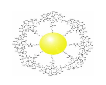
Nanoparticles
|
Figure 3: Nanoparticle
Nanoclusters
As well as the nanoparticles, they have an irregular structure besides being semi-crystalline, but they are tinier than the nanoparticles. Its diameter ranges between 1, and 10 nm.
Also, nanoclusters are sensitive to their size and become more reactive if they increase or decrease proportionally.
Nanocrystals
They are monocrystalline nanostructures, whose size ranges from 1 to 30 nm. Semiconductor nanocrystals are more commonly known as quantum dots.
- One-dimensional nanomaterials (1D)
In the last decade, 1D NSMs have stimulated an increasing interest due to their importance in research, and developments, and have a wide range of potential applications. It is generally accepted that 1D NSMs are ideal systems for exploring a large number of novel phenomena at the nanoscale and investigating the size, and dimensionality dependence of functional properties.
They are also expected to play an important role as both interconnects, and the key units in fabricating electronic, optoelectronic, and EEDs with nanoscale dimensions. The field of 1D NSMs such as nanotubes has attained significant attention. 1D NSMs have a profound impact on nanoelectronics, nanodevices, and systems, nanocomposite materials, alternative energy resources, and national security. We show the 1D NSMs, such as nanowires, nanorods, nanotubes, nanobelts, nanoribbons, and hierarchical nanostructures, which have been synthesized in the laboratories. They have a variable length, conserving two dimensions (height, and width) in the nanometer regime; to these correspond the nanowires and nanotubes.
|
Figure 4: Classification of nanostructured materials
They are elongated crystalline structures whose characteristics stand out for their conductive or semiconducting properties. Nanowires have been obtained from various metallic materials, semiconductors, oxides, etc. In recent years, nanowires have shown special scientific interest due to their potential applications in nanoelectronics, optoelectronics, and sensors.
Nanotubes
- Two-dimensional nanomaterials (2D)
Besides, a 2D NSMs are particularly interesting not only for a basic understanding of the mechanism of nanostructure growth, but also for investigation, and developing novel applications in sensors, photocatalysts, nano-containers, nanoreactors, and templates for 2D structures of other materials.
There are 2D NSMs such as junctions (continuous islands), branched structures, nano-prisms, nanoplates, nanosheets, nanowalls, and nanodisks.
They are nanomaterials formed by very thin layers; thin nanolayers with areas of undefined size, and a thickness between 1, and 100 nm.
Graphene is the most notable example because, due to its multiple, and exceptional properties, it has the potential to revolutionize technology. Its possible applications extend to very diverse areas, ranging from the miniaturization of electronic devices to the elaboration of drugs against cancer in medicine.
SYNTHESIS
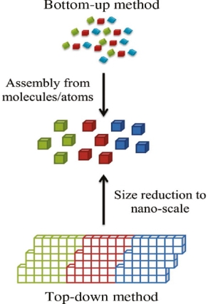
Bottom-up, and top-down approach to the synthesis of nanomaterials
The synthesis of nanomaterials is key to the future success of this new technology. The methods of producing nanoparticles are classified into two main categories: Bottom-up approach
Top-down approach
BOTTOM-UP APPROACH
In bottom-up approaches, nanomaterials are assembled from basic building blocks, such as molecules or nanoclusters. The basic building blocks, in general, are nanoscale objects with suitable properties that can be grown from elemental precursors. The concept of the bottom-up approach is that the complexity of nanoscale components should reside in their self-assembled internal structure, requiring as little intervention as possible in their fabrication from the macroscopic world.
The bottom-up approach uses atomic or molecular feed-stocks as the source of the material to be chemically transformed into larger nanoparticles. This has the advantage of being potentially much more convenient than the top-down approach. By controlling the chemical reactions, and the environment of the growing nanoparticle, then the size, shape, and composition of the nanoparticles may all be affected. For this reason, nanoparticles produced by bottom-up, chemically based, and designed, reactions are normally seen as being of higher quality, and having greater potential applications. This has led to the growth of a host of common bottom-up strategies for the synthesis of nanoparticles. Many of these techniques can be tailored to be performed in gas, liquid, solid states, hence the applicability of bottom-up strategies to a wide range of end products. Most of the bottom-up strategies require suitable organometallic complexes or metal salts to be used as chemical precursors, which are decomposed in a controlled manner resulting in particle nucleation, and growth. One of the key differences that can be used to subdivide these strategies into different categories is the method by which the precursor is decomposed.
A typical example of bottom-up is processing for nanocomposite magnets from individual high-magnetization and high-coercivity nanoparticles. The assembling critically depends on the availability of anisotropic (single crystal) hard magnetic nanoparticles. Anisotropic nanoparticles produced via surfactant-assisted high energy ball milling satisfy the major requirements for this application.
|
Figure 5: Bottom-up, and top-down approach
TOP-DOWN APPROACH
In top-down approaches, the bulk material is restructured (i.e. partially dismantled, machined, processed, or deposited) to form nanomaterials. The aggressive scaling of electronic integrated circuits in recent years can be considered the greatest success of this paradigm. For top-down methods, the challenges increase as device size is reduced, and as the desired component designs become larger and more complex. Also, the top-down assembly of nano components over large areas is difficult and expensive.
The top-down method involves the systematic breakdown of bulk material into smaller units using some form of grinding mechanism. This is beneficial, and simple to execute, and avoids the use of volatile, and poisonous compounds frequently found in the bottom-up techniques. However, the quality of the nanoparticles formed by grinding is accepted to be poor in comparison with the material produced by modern bottom-up methods. The main drawbacks include defect problems from grinding equipment, low particle surface areas, asymmetrical shape, and size distributions, and high energy needed to produce relatively small particles. Apart from these disadvantages, it must be distinguished that the nano-material produced from grinding still finds use, due to the simplicity of its manufacture, in applications including magnetic, catalytic, and structural properties.
Key Takeaways
- Nanotechnology deals with the design, characterization, production, and applications of nanostructures, and nanodevices, and Nanosystems.
- Nanoscience deals with the study of properties of materials at nanoscales where properties differ significantly from those at a larger scale.
- When the material size of the object is reduced to the nanoscale, then it exhibits different properties than the same material in bulk form.
- Nanomaterials can be produced in different dimensionalities.
- One dimensional nanomaterial: Surface coatings, and thin films
- Two-dimensional nanomaterials: nanotubes nanowires, biopolymers
- Three-dimensional nanomaterials: nanoparticles, precipitates, colloids, quantum dots, nanocrystalline materials, fullerenes, or carbon nano-60.
- The methods of producing nanoparticles are classified into two main categories: Bottom-up approach & Top-down approach
a) BALL MILLING
It is a ball milling process where a powder mixture placed in the ball mill is subjected to high-energy collision from the balls. This process was developed by Benjamin and his co-workers at the International Nickel Company in late 1960. A ball mill is a cylindrical device used in grinding (or mixing) materials like ores, chemicals, ceramic raw materials, and paints. It is a type of grinder.
Ball mills rotate around a horizontal axis. It is partially filled with the material to be ground and the grinding medium. Different materials are used as media, including ceramic balls, flint pebbles, and stainless steel balls. An internal cascading effect reduces the material to a fine powder.
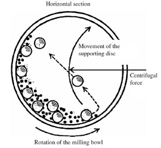
The ball mill system consists of one turn disc (turntable), and two or four bowls. The turn disc rotates in one direction while the bowls rotate in the opposite direction. The centrifugal forces, created by the rotation of the bowl around its axis together with the rotation of the turn disc, are applied to the powder mixture, and milling balls in the bowl. The powder mixture is fractured and cold-welded under high energy impact.
The figure below shows the motions of the balls and the powder. Since the rotation directions of the bowl and turn disc are opposite, the centrifugal forces are alternately synchronized. Thus friction resulted from the hardened milling balls, and the powder mixture being ground alternately rolling on the inner wall of the bowl, and striking the opposite wall. The impact energy of the milling balls in the normal direction attains a value of up to 40 times higher than that due to gravitational acceleration. Hence, the planetary ball mill can be used for high-speed milling.
Figure 6: Ball mill
Industrial ball mills can operate continuously fed at one end, and discharged at the other end. Large to medium-sized ball mills are mechanically rotated on their axis, but small ones normally consist of a cylindrical capped container that sits on two drive shafts (pulleys, and belts are used to transmit rotary motion).
High-energy ball milling
High-quality ball mills are potentially expensive and can grind mixture particles to as small as 0.01 µm. This results in increased surface area, and rate of the reaction.
During the high-energy ball milling process, the powder particles are subjected to high energetic impact.
Micro structurally, the mechanical alloying process can be divided into four stages:
a) Initial stage
b) Intermediate stage
c) Final stage
d) Completion stage
(a) At the initial stage of ball milling, the powder particles are flattened by the compressive forces due to the collision of the balls. Micro-forging leads to changes in the shapes of individual particles, or clusters of particles being impacted repeatedly by the milling balls with high kinetic energy. However, such deformation of the powders shows no net change in mass.
(b) At the intermediate stage of the mechanical alloying process, significant changes occur in comparison with those in the initial stage. Cold welding is now significant. The intimate mixture of the powder constituents decreases the diffusion distance to the micrometer range. Fracturing and cold welding are the dominant milling processes at this stage. Although some dissolution may take place, the chemical composition of the alloyed powder is still not homogeneous.
(c) At the final stage of the mechanical alloying process, considerable refinement, and reduction in particle size is evident. The microstructure of the particle also appears to be more homogenous on a microscopic scale than those at the initial, and intermediate stages. True alloys may have already been formed.
(d) At the completion stage of the mechanical alloying process, the powder particles possess an extremely deformed metastable structure. At this stage, the lamellae are no longer resolvable by optical microscopy. Further mechanical alloying beyond this stage cannot physically improve the dispersoid distribution. Real alloy with a composition similar to the starting constituents is thus formed.
There are many types of grinding media suitable for use in a ball mill, each material having its specific properties, and advantages. Common in some applications is stainless steel balls. While usually very effective due to their high density, and low contamination of the material being processed, stainless steel balls are unsuitable for some applications.
High-energy ball milling, the only top-down approach for nanoparticle synthesis, has been used for the generation of catalytic, magnetic, and structural nanoparticles.
The technique, which is already a commercial technology, has been considered dirty because of contamination problems from ball-milling processes. However, the availability of tungsten carbide components, and the use of inert atmosphere, and/or high vacuum processes have reduced impurities to acceptable levels for many industrial applications.
Common drawbacks include the low surface area, the highly polydisperse size distributions, and the partially amorphous state of the as-prepared powders.
b) SPUTTERING
Sputtering
Sputtering is a physical process in which atoms in a solid-state (target) are released, and pass into the gas phase by bombardment with energetic ions (mainly noble gas ions).
Sputtering is usually understood as the sputter deposition, a high vacuum-based coating technique belonging to the group of PVD processes.
Sputtering is used as a cleaning method for the preparation of high-purity surfaces, and it is also used for analyzing the chemical composition of surfaces.
Sputtering is a mechanism by which atoms are dislodged from the surface of a material as a result of a collision with high-energy particles. Thus, PVD by Sputtering is a term used to refer to a physical vapor deposition (PVD) technique wherein atoms or molecules are ejected from a target material by high-energy particle bombardment so that the ejected atoms or molecules can condense on a substrate as a thin film nano dimension. Sputtering has become one of the most widely used techniques for depositing various metallic films on wafers, including aluminum, aluminum alloys, platinum, gold, TiW, and tungsten.
Process of Sputtering
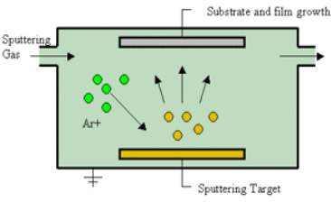
The principle of Sputtering is to use the energy of plasma (partially ionized gas) on the surface of a target (cathode), to pull the atoms of the material one by one, and deposit them on the substrate.
Sputtering as a deposition technique may be described as a sequence of these steps:
1) Ions are generated, and directed at a target material;
2) The ions sputter atoms from the target;
3) The sputtered atoms get transported to the substrate through a region of reduced pressure;, and
4) The sputtered atoms condense on the substrate, forming a thin film.
To do this, plasma is created by the ionization of pure gas. Usually, we take Argon gas. Ionization of a pure gas is done by applying potential difference (pulsed DC), or by electromagnetic excitation.
Thus plasma is composed of Ar+ ions which are accelerated and confined around the target due to the presence of a magnetic field.
Each ionized atom strikes the target, and transfers its energy, and rips an atom, having enough energy to be projected to the substrate.
|
Figure 7: Sputtering
The plasma is created at relatively high pressures (10-1 - 10-3 mbar), but it is necessary to start from a lower pressure before the introduction of Argon, to avoid contamination due to the residual gases.
The diversity of sputtering target shapes (circular, rectangular, Delta, tubular...), and the materials used allows creating all types of thin layers, including alloys during a single run.
Basics of the Sputtering Process
When bombarding a surface with ions, various effects may occur, depending on the ions used, and their kinetic energy:
1. Material is removed from the bombarded target (cathode). This is the sputtering described here.
2. The ions are incorporated into the target material, and enter there, possibly a chemical compound. This effect is then called (reactive) ion implantation.
3. The ions condense on the bombarded substrate, where they form a layer: ion beam deposition.
If a material removal is intended, the ions must have a certain minimum energy. The impinging ion transmits its impulse to atoms of the bombarded material (target), which then - similar to the billiards - trigger further collisions. After several collisions, some of the target atoms have a momentum away from the target interior. If such an atom is sufficiently close to the surface, and has sufficiently high energy, it leaves the target.
The sputter yield depends
- On the kinetic energy, and
- Mass of the ions
- On the binding energy of the surface atoms
- Their mass
To eject an atom from the target, the ions must have material-dependent minimum energy (typically 30-50 eV).
Above this threshold, the yield increases. However, initially, it increases strongly then flattens rapidly.
At high ion energies, this energy is deposited even deeper into the target, and thus barely reaches the surface.
The ratio of the masses of ion and target atom determines the possible momentum transfer. For light target atoms, maximum yield is achieved when the mass of the target and ion approximately match. However, as the mass of the target atoms increases, the maximum of the yield shifts to ever higher mass ratios between the ion, and the target atom.
The ion bombardment generates not only neutral atoms, but also secondary electrons, and, to a lesser extent, secondary ions, and clusters of different masses. The energy distribution of the dissolved atoms has a maximum at half the surface binding energy but falls to high energies only slowly so that the average energy is often an order of magnitude above. This effect is exploited in analysis methods of surface physics, and thin-film technology as well as for the production of thin layers (sputter deposition).
Advantages
1) Sputtering can be achieved from large-size targets, simplifying the deposition of a thin film with uniform thickness over large wafers;
2) Film thickness is easily controlled by fixing the operating parameters, and simply adjusting the deposition time;
3) Control of the alloy composition, as well as other film properties such as step coverage, and grain structure, is more easily accomplished than by deposition through evaporation;
4) Sputter-cleaning of the substrate in a vacuum before film deposition can be done;
5) Device damage from X-rays generated by electron beam evaporation is avoided.
Disadvantages
1) High capital expenses are required;
2) The rates of deposition of some materials (such as SiO2) are relatively low;
3) Some materials such as organic solids are easily degraded by ionic bombardment;
4) Sputtering has a greater tendency to introduce impurities in the substrate than deposition by evaporation because the former operates under a lesser vacuum range than the latter.
c) SOL-GEL TECHNIQUE
SOL-GEL PROCESS
Sol-gel is a low temperature, highly controllable, and cost-effective method for the production of homogeneous, highly stoichiometric, and high-quality ultrafine nanostructures.
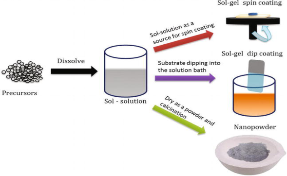
The sol-gel process involves the formation of a colloidal suspension of particles called “sol", and the transition of the colloidal “sol" into a solid called the "gel" phase. The sol-gel process allows the fabrication of thin films with a large variety of properties. Sol-gel chemistry is a remarkably versatile approach for fabricating materials.
The sol is made of solid particles of a diameter of a few hundred nm, usually, inorganic metal salts, suspended in a liquid phase. In a typical sol-gel process, the precursor is subjected to a series of hydrolysis, and polymerization reactions to form a colloidal suspension, and then the particles condense in a new phase, the gel, in which a solid macromolecule is immersed in a solvent.
Sol is obtained by either hydrolysis or polymerization reactions by adding suitable reagents in the precursor solution. The sol can be deposited onto preferred substrates as thin films using two techniques,
(1) spin coating
(2) dip coating
The gelation process done through condensation of the sol or the addition of polymers converts this sol to gel. This gel can be used to form materials of different types such as nanoparticles, xerogel, glass, or ceramics depending upon the further processing steps involved.
|
Figure 8: Schematic diagram of sol-gel processing.
Nanoparticles and xerogels can be obtained by simple evaporation of the solvent. The obtained xerogel can be formed as ceramics by heat treatment, and glassy nature can be induced by melting techniques. Thus, the sol-gel method can be used to obtain different forms of materials, controlled phase, and shape, and size of the derived materials
The parameters that could be controlled in the sol-gel method includes
(1) Concentration of precursor used,
(2) Nature of solvent used,
(3) the pH of the solution,
(4) Type of additives added, and their concentration,
(5) Pre, and post-heat treatment of the materials,
(6) Aging of the solution, and
(7) Nature of polymer used for condensation
The particles formed in the gel matrix possess uniform shape, and size that enhances the optical, electrical, magnetic, and other intrinsic nature of the materials.
Of the factors listed above, pH, nature, and concentration of catalyst, and temperature have been identified as most important. Thus, by controlling these factors, it is possible to vary the structure and properties of the sol-gel-derived inorganic network over wide ranges. The solutions exhibit a strong concentration dependence on the intrinsic viscosity, and a power-law dependence of the reduced viscosity. The sol solution is deposited on the substrates by spraying, dipping, or spinning
d) LASER VAPORIZATION
Laser Vaporization
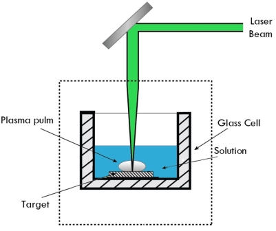
This method involves melting of material to be deposited by a suitable laser, vaporization, and deposition of nanoparticles on the substrates.
If the removal is by vaporization, special attention must be given to the plume.
The plume will be a plasma-like substance consisting of molecular fragments, neutral particles, free electrons, and ions, and chemical reaction products. The plume will be responsible for optical absorption, and scattering of the incident beam, and can condense on the surrounding work material, and/or the beam delivery optics.
If the material to be ablated has poor absorption, such as diamond, but a thermally converted form of the material has relatively good absorption, such as graphite, then it is normal to cover the diamond surface with a thin coating of graphite.
|
Figure 9: Laser Vaporization
The laser will ablate the graphite, and in doing so the surface of the underlying diamond will be converted to graphite allowing efficient absorption. Sequentially, the graphite is ablated, and a new layer of diamond is converted.
The ability of the material to absorb laser energy limits the depth to which that energy can perform useful ablation. The absorption depth of the material, and the heat of vaporization of the work material determine ablation depth.
The depth is also a function of beam energy density, the laser pulse duration, and the laser wavelength. Laser energy per unit area on the work material is measured in terms of the energy fluency.
There are several key parameters to consider for laser ablation.
- The first is a selection of a wavelength with a minimum absorption depth. This will help ensure a high-energy deposition in a small volume for rapid, and complete ablation.
- The second parameter is short pulse duration to maximize peak power and to minimize thermal conduction to the surrounding work material.
- The third parameter is the pulse repetition rate. If the rate is too low, all of the energy which was not used for ablation will leave the ablation zone allowing cooling. If the residual heat can be retained, thus limiting the time for conduction, by a rapid pulse repetition rate, the ablation will be more efficient. More of the incident energy will go toward ablation, and less will be lost to the surrounding work material and the environment.
- The fourth parameter is the beam quality. Beam quality is measured by the brightness (energy), the focus ability, and the homogeneity. The beam energy is of no use if it cannot be properly and efficiently delivered to the ablation region. Further, if the beam is not of controlled size, the ablation region may be larger than desired with the excessive slope in the sidewalls.
e) ELECTRO DEPOSITION
Electro Deposition
The electrodeposition technique is used to electroplate a material.
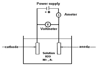
Current is passed through electrolytes such as aqueous solutions of salts, acids, etc. Two electrodes were immersed inside the electrolyte. When current is passed through electrolytes certain mass of the substance liberated at one electrode gets deposited on the surface of the other.
By controlling the current, and other parameters, it is possible to deposit even a single layer of atoms. Nanostructured films of copper, platinum, nickel, gold, etc., can be produced by electrodeposition.
The film thus obtained is mechanically robust, highly flat, and uniform. Since these films have larger surface areas, they exhibit quite different, and favourable electrical properties. They have a wide range of applications. These include batteries, fuel cells, solar cells, magnetic read heads, etc.
|
Figure 10: Electro Deposition
The electrolyte contains positive and negative ions. Therefore, it is considered an ionic conductor. To prepare an electrolyte, the desired metal contained in a chemical species liquidized (mostly dissolved in water) to form a molten salt besides different organic, and ionic liquids are currently used for particular electroplating processes.
To begin electrodeposition, the cathode (working electrode, W.E) is immersed in the electrolyte contained in a vessel (cell) along with the anode (counter electrode, C.E). To allow electric current flow in the circuit, the two electrodes are connected to a battery or any other power source. The cathode is connected to the negative terminal of the battery, while the anode is connected to the positive terminal so that the metal ions are reduced to metal atoms, which eventually form the deposit on the surface. Figure 10 shows a schematic presentation of an electrolytic cell for electroplating or electrodepositing a metal “M” from an aqueous (water) solution of metal salt “MA”.
This type of circuit arrangement directs electrons into a bath from the power supply to the cathode. In the bath, the electric current is carried by the positively charged ions from the anode toward the negatively charged cathode. This enables the metal ions in the bath to migrate toward extra electrons that are located at or near the surface of the cathode. Finally, the metal ions are removed from the solution and are deposited on the surface of the object as a thin layer. The reaction in the aqueous medium at the cathode, therefore, obeys equation 1:
M+n + ne− → M ………..(1)
|
where n is the number of electrons involved in the reaction.
The thickness of the electrodeposited layer on the substrate is determined by the time duration of the plating. The longer the object remains in the chemical bath, the thicker the deposited layer is.
The process itself is simple, a conductive surface is immersed into an electrolyte containing ions of the material to be deposited, and a voltage is applied across this solid/electrolyte interface, resulting in a charge transfer reaction, and film deposition. The driving force for this process is the applied potential, a quantity that can be easily, and precisely controlled down to the mV, and over timescales as short as 1ns. This feature leads to considerable control over the material formation process, its microstructure, and properties.
The challenge in developing electrodeposition processes today is not the synthesis of a predefined material, but to strike a compromise between the ideal conditions used to produce this material, and the commercial feasibility of the process.
Advantages of electrodeposition
- The high utilization rate of the raw materials
- Low energy consumption
- Low material waste
- Little capital investment
- Ease of implementation
Polymers, and biomaterials are electrodeposited for biomedical applications; metal oxides, and compound semiconductors are grown electrochemically for electronic or optoelectronic applications.
Electrodeposition in new electrolytic media such as ionic liquids or supercritical fluids is being strongly pursued with some success. Electrodeposition plays an important role in the development of sustainable energy conversion technologies, both at the portable, and on a global scale. It is facilitating the development of large-scale manufacturing processes
f) CHEMICAL VAPOUR DEPOSITION
Chemical Vapour Deposition (CVD)
Chemical Vapour Deposition (CVD) refers to the formation of a non-volatile solid film of nano dimension on a substrate from the reaction of vapour phase chemical reactants containing the right constituents.
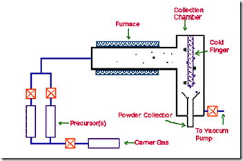
A reaction chamber is used for this process, into which the reactant gases are introduced to decompose and react with the substrate to form the film of nano dimensions. Chemical vapour deposition is used in a multitude of semiconductor wafer fabrication processes, including the production of amorphous, and polycrystalline thin films (such as polycrystalline silicon), deposition of SiO2 (CVD SiO2), and silicon nitride, and growing of single-crystal silicon epitaxial layers.
A typical CVD system consists of the following parts:
1) Sources of, and feed lines for gases;
2) Mass flow controllers for metering the gases into the system;
3) A reaction chamber or reactor;
4) A system for heating the wafer on which the film is to be deposited; and
5) Temperature sensors.
|
Figure 11: Chemical Vapour Deposition (CVD)
In this technique, the precursor vapour is passed through a hot walled reactor. The precursor decomposes, and nanoparticles nucleate in the gas phase. The nanoparticles are carried by the gas stream and collected on a cold finger. The size of the nanoparticles is determined by the particle residence time, temperature of the chamber, precursor composition, and pressure.
A basic CVD process consists of the following steps:
1) A predefined mix of reactant gases, and diluents inert gases are introduced at a specified flow rate into the reaction chamber;
2) The gas species move to the substrate;
3) The reactants get adsorbed on the surface of the substrate;
4) The reactants undergo chemical reactions with the substrate to form the film; and
5) The gaseous by-products of the reactions are desorbed and evacuated from the reaction chamber.
During the process of chemical vapour deposition, the reactant gases not only react with the substrate material at the wafer surface (or very close to it) but also in the gas phase in the reactor's atmosphere. Reactions that take place at the substrate surface are known as heterogeneous reactions, and are selectively occurring on the heated surface of the wafer where they create good- quality films of nano dimensions.
Reactions that take place in the gas phase are known as homogeneous reactions. Homogeneous reactions from gas-phase aggregates of the depositing material, which adhere to the surface poorly, and at the same time form low-density films with lots of defects. In short, heterogeneous reactions are much more desirable than homogeneous reactions during chemical vapour deposition.
Key Takeaways
- It is a ball milling process where a powder mixture placed in the ball mill is subjected to high-energy collision from the balls. It is a type of grinder.
- The ball mill system consists of one turn disc (turntable), and two or four bowls.
- Sputtering is a physical process in which atoms in a solid-state (target) are released, and pass into the gas phase by bombardment with energetic ions (mainly noble gas ions).
- The sol-gel process involves the formation of a colloidal suspension of particles called “sol", and the transition of the colloidal “sol" into a solid called the "gel" phase.
- The sol can be deposited onto preferred substrates as thin films using two techniques are spin coating and dip coating.
- Laser Vaporization method involves melting of material to be deposited by a suitable laser, vaporization, and deposition of nanoparticles on the substrates.
- The electrodeposition technique is used to electroplate a material. Current is passed through electrolytes such as aqueous solutions of salts, acids, etc. Two electrodes were immersed inside the electrolyte. When current is passed through electrolytes certain mass of the substance liberated at one electrode gets deposited on the surface of the other.
- Chemical Vapour Deposition (CVD) refers to the formation of a non-volatile solid film of nano dimension on a substrate from the reaction of vapour phase chemical reactants containing the right constituents.
- Scanning electron microscopy has been applied to the surface studies of metals, ceramics, polymers, composites, and biological materials for both topography as well as compositional analysis.
- An extension of this technique is Electron Probe Micro Analysis (EPMA), where the emission of X-rays, from the sample surface, is studied upon exposure to a beam of high-energy electrons.
- Depending on the type of detectors used this method is classified into two as Energy Dispersive Spectrometry (EDS), and Wavelength Dispersive Spectrometry (WDS). This technique is used extensively in the analysis of metallic, and ceramic inclusions, inclusions in polymeric materials, and diffusion profiles in electronic components.
Nanomaterials possess unique, and beneficial, physical, chemical, and mechanical properties; they can be used for a wide variety of applications.
Material technology
- Nanocrystalline aerogel is lightweight and porous, so they are used for insulation in offices homes, etc.
- Cutting tools made of Nanocrystalline materials are much harder, much more wear-resistant, and last stranger.
- Nanocrystalline material sensors are used for smoke detectors, ice detectors on aircraft wings, etc.
- Nanocrystalline materials are used for high energy density storage batteries.
- Nanosized titanium dioxide and zinc dioxide are used in sunscreens to absorb and reflect ultraviolet rays.
- Nanocoating of highly activated titanium dioxide acts as water repellent, and antibacterial.
- The hardness of metals can be predominately enhanced by using nanoparticles.
- Nanoparticles in paints change colour in response to change in temperature or chemical environment, and reduce infrared absorption, and heat loss.
- Nanocrystalline ceramics are used in the automotive industry as high strength springs, ball bearings, and valve lifters.
Information technology
- Nanoscale fabricated magnetic materials are used in data storage
- Nanocomputer chips reduce the size of the computer.
- Nanocrystalline starting light-emitting phosphors are used for flat panel displays.
- Nanoparticles are used for information storage.
- Nanophotonic crystals are used in chemical optical computers.
Biomedical
- Biosensitive nanomaterials are used for ragging of DNA, and DNA chips.
- In the medical field, nanomaterials are used for disease diagnosis, drug delivery, and molecular imaging.
- Nanocrystalline silicon carbide is used for artificial heart valves due to its low weight, and high strength.
Energy storage
- Nanoparticles are used in hydrogen storage.
- Nanoparticles are used in magnetic refrigeration.
- Metal nanoparticles are useful in the fabrication of ionic batteries.
- Nanomaterials possess unique, and beneficial, physical, chemical, and mechanical properties; they can be used for a wide variety of applications.
Material technology
- Nanocrystalline aerogels are lightweight and porous, so they are used for insulation in offices homes, etc.
- Cutting tools made of Nanocrystalline materials are much harder, much more wear-resistant, and last stranger.
- Nanocrystalline material sensors are used for smoke detectors, ice detectors on aircraft wings, etc.
- Nanocrystalline materials are used for high energy density storage batteries.
- Nanosized titanium dioxide and zinc dioxide are used in sunscreens to absorb and reflect ultraviolet rays.
- Nanocoating of highly activated titanium dioxide acts as water repellent, and antibacterial.
- The hardness of metals can be predominately enhanced by using nanoparticles.
- Nanoparticles in paints change colour in response to change in temperature or chemical environment, and reduce infrared absorption, and heat loss.
- Nanocrystalline ceramics are used in the automotive industry as high strength springs, ball bearings, and valve lifters.
Information technology
- Nanoscale fabricated magnetic materials are used in data storage
- Nanocomputer chips reduce the size of the computer.
- Nanocrystalline starting light-emitting phosphors are used for flat panel displays.
- Nanoparticles are used for information storage.
- Nanophotonic crystals are used in chemical optical computers.
Biomedical
- Biosensitive nanomaterials are used for ragging of DNA, and DNA chips.
- In the medical field, nanomaterials are used for disease diagnosis, drug delivery, and molecular imaging.
- Nanocrystalline silicon carbide is used for artificial heart valves due to its low weight, and high strength.
Energy storage
- Nanoparticles are used in hydrogen storage.
- Nanoparticles are used in magnetic refrigeration.
- Metal nanoparticles are useful in the fabrication of ionic batteries.
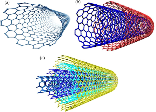
A tube may contain one cylindrical wall of graphite or several concentric cylindrical walls. A carbon nanotube consisting of one cylindrical graphite is called a single-walled nanotube. Otherwise, they are known as multi-walled nanotubes.
TYPES OF CNT
Since then, carbon nanotubes with various structures have been discovered. According to the number of graphic shells, they are mainly categorized as single-walled (SWNTs), Double-walled carbon nanotubes (DWCNTs), and multi-walled carbon nanotubes (MWNTs).
|
Figure 12: Types of CNT
Single-Walled Carbon Nanotubes (SWNTs)
Single-wall carbon nanotubes
SWNTs are known as Single-wall carbon nanotubes. SWNTs are one-dimensional materials. It is considered a special class of carbon materials.
They are formed by rolling the sheet of graphene. They form the shape of hollow tubes. The wall of the tube has the thickness of a single atom.
This material shows exceptional mechanical, electrical, thermal, and optical properties because of its chemical structure, and dimensional limits. Carbon nanotubes have become of great interest for both stand-alone studies, and for use in composite materials.
Single-wall carbon nanotubes can be described as a long tube formed by wrapping a single graphene sheet into a cylinder with a diameter of about 1 nanometre. There is capping on ends by fullerene cages.
The fullerene structures form the surface with the desired curvature to enclose the volume. The fullerene structures combine with alternating structures of five hexagons adjacent to one pentagon, and the sidewalls of carbon nanotubes are made of graphene sheets consisting of neighbouring hexagonal cells.
If we take other polygon structures like pentagons, and heptagons, they constitute defects of sidewalls. The different cylindrical structure can be produced just by rolling the SWNTs in different directions. The entire properties of the SWNTs and their structure get changed.
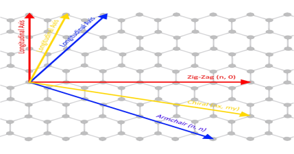
Due to cylindrical symmetry, there are only a handful of methods that are effective in making seamless cylinders, and they are characterized by the chiral vectors with integer indices (n, m).
To establish the chiral vector, two atoms in the graphene sheet are selected, with one serving as the origin of the vector pointing toward the other atom. The graphene sheet is then rolled in a way that allows the two atoms to coincide.
Under these circumstances, the chiral vectors form a plane perpendicular to the longitude direction of nanotubes, and the lengths of the chiral vectors are equal to the circumference.
Three different types of SWNTs are distinctly characterized, named “zigzag” (m = 0), “armchair” (n = m), and “chiral.”
Because of the change in structure, the entire properties of the nanotubes get change. These structural variations also result in differences in electrical conductivity, and mechanical strength.
|
The electrical properties of carbon nanotubes are dependent upon the orientation of the lattice. The lattice orientation is given by two parameters (n, m). The image to the right shows how the n, and m orientations relate to the longitudinal axis of the nanotube, and the rotational axis. There are typically three types of nanotubes that can form, these are the armchair (where n = m), zig-zag (n=x, m=0), and chiral (n=x, m=y).
Carbon nanotubes can exhibit either metallic properties or semiconducting properties, depending upon the orientation of the lattice. Zig-zag and armchair carbon nanotubes exhibit metallic properties, whilst chiral nanotubes can be either metallic or semiconducting depending upon the difference between the n, and m units.
In addition to this ability to exhibit both metallic, and semiconducting electronic structures carbon nanotubes offer exceptional charge carrier mobilities, this is due to the combination of the delocalization of electrons across the lattice, and the small dimensions in the radial axis constraining movement of charge carriers along the longitudinal axis of the tubes.
Double-walled carbon nanotubes (DWCNTs)
Double-walled carbon nanotubes (DWCNTs) also belong to the family of one-dimensional material. Double-walled carbon nanotubes (DWCNTs) similar to single-walled carbon nanotubes. The difference is Double-walled carbon nanotubes consist of two nanotubes, with one nested within the other. The differences in the diameters of the two nanotubes can be controlled by varying degrees of interaction between the two tubes.
DWCNTs consist of two individual carbon nanotubes, with one embedded inside the other. The differences in diameters and the chirality of the two different nanotubes lead to a varying degree of interaction between the two.
But the properties of the individual nanotubes are different from one another. It is this wide variety of possibilities that have made DWCNTs a focus of interest for carbon nanotube research.
The chirality determines whether the nanotube will be semiconducting or metallic. By Varying chirality, we can allow a range of inner-wall outer-wall interactions to occur.
It is possible to achieve metallic-metallic, semiconducting-metallic, metallic-semiconducting, or semiconducting-semiconducting interactions. In addition to this, the metallic, and semiconducting properties can vary depending upon the exact lattice parameters, which enables a wide range of possible property combinations.
it is possible to modify the outer nanotube without changing the properties of the inner nanotube, this is one of the best advantages over single-walled carbon nanotubes.
This modification could be either through functionalization (to add solubilizing groups), or the doping of the structure (to alter the properties). This allows the double-walled system to maintain the functionality of a single-walled nanotube whilst simultaneously having the solubility of functionalized nanotubes. This combination makes double-walled systems attractive for use as additives in composite materials as it allows high doping concentrations without affecting the properties of the nanotube overall.
The biggest barriers are the synthesis and purification of DWCTs. DWCNTs can be synthesis by arc discharge or catalytic chemical vapour deposition. The remainder of the nanotubes synthesized using these techniques are a mixture of single-walled, and multi-walled nanotubes which then need to be purified to obtain individual double-walled nanotubes. The process of purification is much more difficult.
Methods such as high-temperature oxidation result in the preferential oxidation of single-walled nanotubes over double-walled ones. However, the process can damage the remaining nanotubes and will leave residual multi-walled contaminants behind.
Other processes, such as ultra-centrifugation, can be used to obtain high-purity DWCNT samples and sort double-walled samples by outer diameter. However this process is labour, and time-intensive making commercialization, and large-scale production of high purity DWCNTs difficult.
Just like with single-walled carbon nanotubes, there are many different areas in which DWCNT's can be applied due to their impressive mechanical, and electrical properties.
Besides, double-walled nanotubes show an increase in mechanical strength, thermal stability, and also chemical stability over that of single-walled nanotubes. However, the ability to combine different nanotube types have the potential to result in interesting optical, electronic, and mechanical properties that are not possible with single-walled nanotubes.
Multi-walled carbon nanotubes (MWCNTs)
Multi-walled carbon nanotubes (MWCNTs) are a special form of carbon nanotubes. In multiple single-walled carbon nanotubes are nested inside one another. Although MWCNTs are still classed as a 1-dimensional form of carbon, the unique properties that are seen within single-walled, and double-walled carbon nanotubes are not as prominent.
MWCNTs consist of multiple carbon nanotubes nested within one another. The number of nanotubes that are within an MWCNT can vary from 3 to 20. At the same time, the diameter of both the internal nanotube and the external most nanotube can vary - from 2nm for the innermost tube to over 50nm for the outer wall.
Just like single-walled nanotubes, they exhibit exceptional electrical, thermal, and mechanical properties. However, due to the increased number of walls, there is a higher likelihood of defects being present compared to single-walled nanotubes - resulting in reduced performances. The outer walls of MWCNTs can be modified with functional groups such as hydroxides, carboxylic acids, or amides to produce additional functionality.
MWCNTs can be produced in high quantities, and are easier to purify (in comparison to single-walled, and double-walled nanotubes). This makes their production costs significantly lower, and is a reason for their adoption in multiple areas of scientific research.
Applications of MWCNTs have been mainly focused on their use in composites where they can be used as an additive. either to:
i) improve the mechanical properties of a material
ii) To improve the electrical properties of a material.
Aside from being used as additives, functionalized MWCNTs are being utilized in a variety of medical, and biotechnological applications. This is due to their high biocompatibility of carbon nanotubes, and the ability to attach specific proteins to functional groups. This can provide a wide variety of targeted therapies such as drug delivery, localized heating for triggering cell death, or even miniature biosensors for in-situ measurements.
Key Takeaways
- Carbon nanotubes are obtained by rolling the graphite sheet into tubes with the bonds at the ends of the sheet.
- Carbon nanotubes are mainly categorized as single-walled (SWNTs), Double-walled carbon nanotubes (DWCNTs), and multi-walled carbon nanotubes (MWNTs).
- SWNTs are known as Single-wall carbon nanotubes. SWNTs are one-dimensional materials. They are formed by rolling the sheet of graphene. They form the shape of hollow tubes. The wall of the tube has the thickness of a single atom.
- Three different types of SWNTs are distinctly characterized, named “zigzag” (m = 0), “armchair” (n = m), and “chiral.”
- DWCNTs consist of two individual carbon nanotubes, with one embedded inside the other. The differences in diameters and the chirality of the two different nanotubes lead to a varying degree of interaction between the two.
- MWCNTs consist of multiple carbon nanotubes nested within one another. The number of nanotubes that are within an MWCNT can vary from 3 to 20. At the same time, the diameter of both the internal nanotube and the external most nanotube can vary - from 2nm for the innermost tube to over 50nm for the outer wall.
Properties of carbon nanotubes
Electrical conductivity: Generally the carbon nanotubes are produced both in metallic, and semiconducting in their electrical behaviour. The conductivity of multi-walled nanotube is more complex. The conductivity and resistivity of ropes of single-walled carbon nanotubes have been measured by placing the electrodes at different parts of the carbon nanotubes. The resistivity of single-walled carbon nanotube ropes was of the order of 10-4 ohm-cm at 270. This means that the conductivity of single-walled nanotube ropes is the most conductive carbon fibres known.
Magnetic property: The carbon nanotube displays the magneto-resistive effects at lower temperatures i.e., the resistance of the carbon nanotube is changed by the application of a dc magnetic field. The variation of resistance in carbon nanotube at 2.3K and 0.36k w.r.t magnetic field is observed. This shows the magneto-resistance effect is negative. This is due to the decrease in resistance with an increase in a magnetic field.
Highly absorbent: The carbon nanotubes have a large surface area and high absorbance. So the carbon nanotubes are used in the air, gas, and water filtration.
Mechanical properties: The strength of the sp2 carbon-carbon bonds gives carbon nanotubes amazing mechanical properties. The stiffness of the material is measured in terms of its Young’s modulus. The Young’s modulus value of single-walled nanotube is about 1Tera Pascal, which is approximately 5 times greater than steel. The tensile strength or breaking strain of nanotube is about 150GPa, which is approximately 150 times greater than steel
Vibration properties: Similar to carbon dioxide molecules, Carbon nanotubes have two normal modes of vibration (a set of vibrational motions known as a normal mode of vibrations). The different modes of vibrational motion are determined from the symmetry of the molecule. In the first mode the diameter of the carbon nanotube moves in, and out at the frequency of 165 cm-1. In the second mode, the carbon nanotube crushing in one direction, and expansion takes place in the perpendicular direction. Thus, it oscillates between sphere and ellipse at a frequency of 17 cm-1. The frequency of the vibration modes depends on the diameter of the nanotube.
i) Energy Storage
Carbon nanotubes are used as electrodes in batteries, and capacitors because they have the characteristics which are required in this kind of material.
The surface area of carbon nanotube is very high and has good electrical conductivity. Also, CNTs have simple, and linear geometry. Because of these properties surface of CNTs is highly accessible to the electrolyte.
CNTs have high thermal conductivity too; therefore CNTs also have applications in a variety of fuel cell components. CNTs high surface area, and high thermal conductivity which makes them useful as electrode catalyst supports in PEM fuel cells.
Because of CNT's high electrical conductivity, they are used in gas diffusion layers and current collectors.
ii) Molecular Electronics
CNTs also playing an important part in molecular electronics. In electronic circuits especially when the size of dimensions reduces to the nanoscale, the interconnections between switches and other active devices become an essential part.
Because of CNTs high electrical conductivity, and its geometry, these are very much suitable molecular electronics
iii) Thermal Materials
CNTs have high heat conductivity and high electrical conductivity. CNTs also show good mechanical properties. So they are considered one of the best electron field-emitter possible.
The record-setting anisotropic thermal conductivity of CNTs is enabling many applications where heat needs to move from one place to another
As we know that CNTs are polymers of pure carbon, and using the rich chemistry of carbon CNTs can be reacted, and manipulated
If we see the molecular structure of CNTs, they are considered molecularly perfect. This implies that they are normally free of property degrading flaws in the nanotube structure.
CNTs have high heat conductivity, high electrical conductivity, and the incredible sharpness of their tip. So this is obvious that these are considered the best field emitters of any material.
The reason for using property like the sharpness of their tip because the smaller the tip’s radius of curvature, the more concentrated will be the electric field which leads to an increase in the field emission.
Lightning rods are sharp because of the same reason.
The sharpness of the tip also implies that they emit a very low voltage, an important fact for building low-power electrical devices that utilize this feature.
CNTs can carry an astonishingly high current density, possibly as high as 1013 A/cm2. But the current we obtaining is very much stable.
An immediate application of this behaviour receiving considerable interest is in field-emission flat-panel displays. Instead of a single electron gun, as in a traditional cathode ray tube display, in CNT-based displays, there is a separate electron gun (or even many of them) for each pixel in the display.
Other applications utilizing the field-emission characteristics of CNTs include general types of low-voltage cold-cathode lighting sources, lightning arrestors, and electron microscope sources.
Their high current density, low turn-on, and operating voltages, and steady, long-lived behaviour make CNTs very attractive field emitters in this application.
v) Fabrics, and Fibers
CNTs also use in the fabric industry. Fibers spun of pure CNTs along with CNT composite fibers have recently been established, and are undergoing speedy development. These fibres are super strong. Because of this, they are widely used in many applications including body, and transmission line cables, woven fabrics vehicle armor, and textiles.
CNTs are also useful in biomedical applications. The reason for using carbon nanotubes in biomedical is a large part of the human body consists of carbon. It is generally considered a great thought of using CNTs in the medical field.
The experimental result shows that Cells have no toxic effect when they are grown on CNTs. The cells also do not adhere to the CNTs.
This is giving rise to applications such as coatings for prosthetics, as well as anti-fouling coatings for ships.
It has also been demonstrated that a single strand of DNA can be bonded to a nanotube, which can then be successfully inserted into a cell.
The ability to functionalize (chemically modify) the sidewalls of CNTs also leads to biomedical applications such as vascular stents, and neuron growth, and regeneration.
vii) CNTs Air, and Water Filtration
Many researchers and corporations have already developed CNT which can be used as an air, and water filtration device. It has been reported that these filters can not only block the smallest particles but also kill most bacteria. This is another area where CNTs have already been commercialized, and products are on the market now.
Their geometry, electrical conductivity, and ability to be precisely derived, make CNTs the ideal choice for the connections in molecular electronics. Besides, they have been demonstrated as switches themselves.
There are a wealth of other potential applications for CNTs, such as solar collection; nanoporous filters; catalyst supports;, and coatings of all sorts.
viii) Structural Materials
These extraordinary characteristics give CNTs potential in numerous applications. The extraordinary properties of CNTs are not restricted to thermal, and electrical conductivities but also include mechanical properties such as toughness, strength, and stiffness.
These properties lead to several applications exploiting them, including advanced composites requiring high values of one or more of these properties.
ix) Catalyst Supports
We already know that the surface area of carbon nanotube is very high. For a Single-wall nanotube, every atom is not just on one surface but each atom is present on two surfaces that are both the inside, and outside of the nanotube.
The ability to attach essentially any chemical species to their sidewalls provides an opportunity for unique catalyst supports. Their electrical conductivity may also be exploited in the search for new catalysts, and catalytic behaviour.
Reference Books
- Nanotechnology, Principles, and Practices Dr. S.K. Kulkarni, Capital publishing Co., New Delhi.
- Engineering Physics-II by M.N.Avadhanulu, and P.G.Kshirsagar
- Engineering physics- Gaur, and Gupta, & S.Chand Publication
- Engineering physics - Avadhanalu, and Kshirsagar, S.Chand Publication
- Engineering physics- Hitendra K Malik, A.K.Singh, Tata McGraw Hill Education Private Limited, New Delhi

