UNIT 4
SEMICONDUCTORS AND MODERN PHYSICS
Semiconductors
Semiconductors are materials that have a conductivity between conductors and insulators.
Semiconductors can be pure elements, such as silicon or germanium, or compounds such as gallium arsenide or cadmium selenide.
They are not good conductors nor good insulators as their name “semi”-conductors.
These materials such as silicon (Si), germanium (Ge), and gallium arsenide (GaAs), have electrical properties somewhere in the middle, between those of a “conductor” and an “insulator”.
They have very few “free electrons” because their atoms are closely grouped in a crystalline pattern called a “crystal lattice” but electrons are still able to flow, but only under special conditions.
The Band Model
Bands are formed by the closely spaced orbitals.
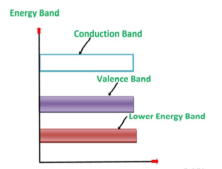
There are three types of bands:
1. Valance Bands: A valence band is a group of orbitals that contain electrons in the shell. Or we can say It is also defined as the energy band that comprises of valence electrons present in the outermost shell of an atomic structure.
These valence electrons, when provided with sufficient energy, get changed into free electrons and moves to the conduction band thereby causing conductivity. It is at a lower energy level than the conduction band in the energy level diagram.
2. Conduction Band: A conduction band is a group of empty orbitals of the shells that do not contain any electron due to their configuration making the orbitals of higher energy levels.
When the electrons pass from the valance band to the conduction band these solids conduct electricity with the flow of charges in the form of electrons.
3. Forbidden Energy Band: These two bands are separated by a certain amount of energy known as the forbidden energy gap. In this band not a single electron is available. Its diagram is named Band Gap.
Let us distinguish between conductors, semiconductors, and insulators based on these bands.
|
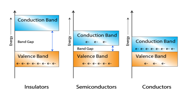
Figure 1: Conductors, Semiconductors, and Insulators based on these bands.
- In Conductors: The valance band and the conduction band overlap each other. This makes it easy for electricity to pass through them. In conductors, the valence band is either not fully occupied with electrons, or the filled valence band overlaps with the empty conduction band. In general, both states occur at the same time, the electrons can therefore move inside the partially filled valence band or inside the two overlapping bands. In conductors, there is no bandgap between the valence band and conduction band.
- In Semi-conductors: there is a slight gap between the conduction band and the valance band. This bandgap is less than or equal to 1.4 eV. The electrons from the valance shell take a little energy to excite from the valance band to the conduction band. Even in semiconductors, there is a bandgap, but compared to insulators it is so small that even at room temperature electrons from the valence band can be lifted into the conduction band. The electrons can move freely and act as charge carriers.
- In Insulators: In insulators, the valence band is fully occupied with electrons due to the covalent bonds. To achieve conductivity, electrons from the valence band have to move into the conduction band. the energy gap is considerably large and the electrons of the valance band cannot be excited to the conduction band before the melting or the dissociation of the solid. This means that under the practically ambient condition it cannot conduct electricity.
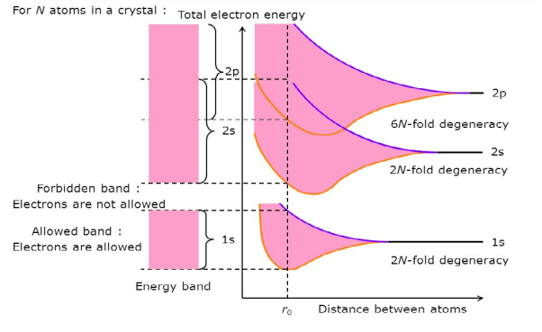
Consider an isolated silicon atom; its energy levels are quantized. When two identical atoms are brought closer together, the quantized energy levels hybridize and split into two different levels because of the mutual interaction of the two atoms. More generally, when N atoms are moved closer until they reach the equilibrium inter-atomic distance d, the energy levels split into N levels. These N levels are very close to each other if N is large (which is the case in a crystal) so that they eventually form a continuous energy band.
|
Figure 2: Formation of Energy band as a function of interatomic distance (distance between atoms)
Key Takeaways
- Semiconductors are materials that have conductivity between conductors and insulators.
- Bands are formed by the closely spaced orbitals.
- There are three types of bands: Valence band, conduction band, Forbidden Energy Band
- On the basis of band theory we can classify the materials as conductors, semiconductors, and insulators based on these bands.
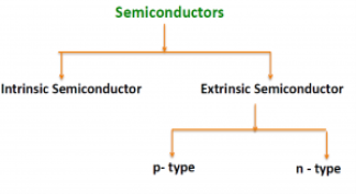
There are two basic groups or classifications that can be used to define the different semiconductor types:
- Intrinsic Semiconductor
- Extrinsic Semiconductor
|
Figure 3: Type of semiconductor
The semiconductor is divided into two types. One is an Intrinsic Semiconductor and the other is an Extrinsic semiconductor. The pure form of the semiconductor is known as the intrinsic semiconductor and the semiconductor in which intentional impurities are added for making it conductive is known as the extrinsic semiconductor.
The conductivity of the intrinsic semiconductor becomes zero at room temperature while the extrinsic semiconductor is very little conductive at room temperature. The detailed explanation of the two types of the semiconductor is given below.
INTRINSIC SEMICONDUCTOR
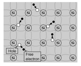
An intrinsic type of semiconductor material made to be very pure chemically. As a result, it possesses a very low conductivity level having very few charge carriers, namely holes and electrons, which it possesses in equal quantities.
|
Figure 4: Intrinsic Semiconductor
The most commonly used semiconductor basics material by far is silicon. Silicon has four valence electrons in its outermost shell which it shares with its neighbouring silicon atoms to form a full orbital of eight electrons. The structure of the bond between the two silicon atoms is such that each atom shares one electron with its neighbour making the bond very stable.
As there are very few free electrons available to move around the silicon crystal, crystals of pure silicon (or germanium) are therefore good insulators. Silicon atoms are arranged in a definite symmetrical pattern making them a crystalline solid structure. A crystal of pure silica (silicon dioxide or glass) is generally said to be an intrinsic crystal (it has no impurities) and therefore has no free electrons.
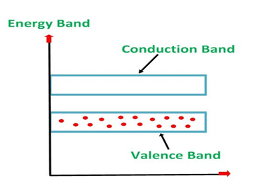
An extremely pure semiconductor is called an Intrinsic Semiconductor. Based on the energy band phenomenon, an intrinsic semiconductor at absolute zero temperature is shown below.
|
Figure 5: Intrinsic semiconductor at absolute zero temperature.
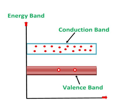
Its valence band is filled and the conduction band is empty. When the temperature is raised and some heat energy is supplied to it, some of the valence electrons are lifted to the conduction band leaving behind holes in the valence band as shown below.
|
Figure 6: Intrinsic semiconductor at T >0
A hole is the absence of an electron in a particular place in an atom. Although it is not a physical particle in the same sense as an electron, a hole can be passed from atom to atom in a semiconductor material. It is considered to have a positive charge. Holes are positive charge carriers.
The electrons reaching the conduction band move randomly. The holes created in the crystal also free to move anywhere.
This behaviour of the semiconductor shows that they have a negative temperature coefficient of resistance. This means that with the increase in temperature, the resistivity of the material decreases, and the conductivity increases.
But simply connecting a silicon crystal to a battery supply is not enough to extract an electric current from it. To do that we need to create a “positive” and a “negative” pole within the silicon allowing electrons and therefore electric current to flow out of the silicon. These poles are created by doping the silicon with certain impurities.
The process by which an impurity is added to a semiconductor is known as Doping. The amount and type of impurity which is to be added to the material have to be closely controlled during the preparation of extrinsic semiconductor. Generally, one impurity atom is added to 108 atoms of a semiconductor.
The purpose of adding impurity in the semiconductor crystal is to increase the number of free electrons or holes to make it conductive.
If a Pentavalent impurity, having five valence electrons is added to a pure semiconductor a large number of free electrons will exist. Which makes an n-type extrinsic semiconductor.
If a trivalent impurity having three valence electrons is added, a large number of holes will exist in the semiconductor. Which makes a p-type extrinsic semiconductor.
EXTRINSIC SEMICONDUCTOR
Extrinsic types of semiconductors are those where a small amount of impurity has been added to the basic intrinsic material. This 'doping' uses an element from a different periodic table group and in this way, it will either have more or fewer electrons in the valence band than the semiconductor itself. This creates either an excess or shortage of electrons. In this way two types of semiconductors are available: Electrons are negatively charged carriers. Holes are positively charged carriers.
Depending upon the type of impurity added the extrinsic semiconductor may be classified as an n-type semiconductor and p-type semiconductor.
P-TYPE EXTRINSIC SEMICONDUCTOR
The extrinsic p-Type Semiconductor is formed when a trivalent impurity is added to a pure semiconductor in a small amount, and as a result, a large number of holes are created in it. A large number of holes are provided in the semiconductor material by the addition of trivalent impurities like Gallium and Indium. Such type of impurities which produce a p-type semiconductor is known as an Acceptor Impurities because each atom of them creates one hole which can accept one electron.
In a P-type semiconductor material, there is a shortage of electrons, i.e. there are 'holes' in the crystal lattice. Electrons may move from one empty position to another and in this case, it can be considered that the holes are moving. This can happen under the influence of a potential difference and the holes can be seen to flow in one direction resulting in an electric current flow. It is harder for holes to move than for free electrons to move and therefore the mobility of holes is less than that of free electrons. Holes are positively charged carriers.
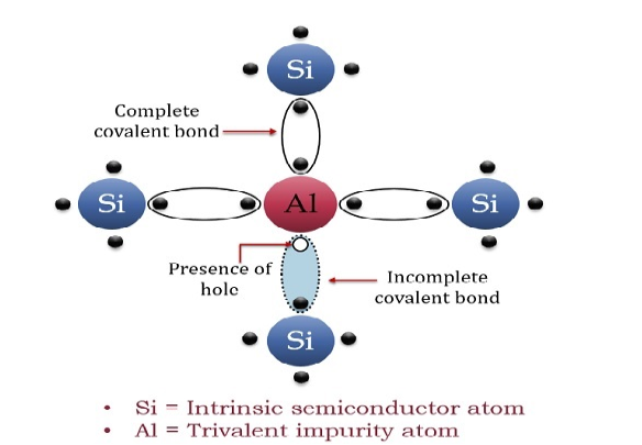
A trivalent impurity like Aluminium, having three valence electrons is added to Silicon crystal in a small amount. Each atom of the impurity fits in the Silicon crystal in such a way that its three valence electrons form covalent bonds with the three surrounding Silicon atoms as shown in the figure below.
|
Figure 7: p-Type Semiconductor
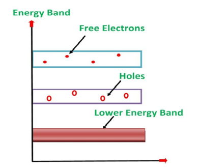
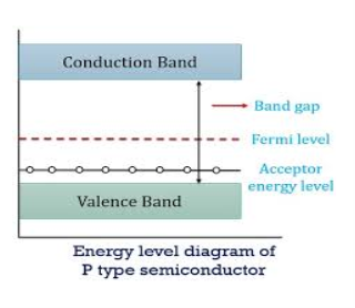
ENERGY BAND DIAGRAM OF P-TYPE SEMICONDUCTOR
The energy band diagram of a p-Type Semiconductor is shown below.
|
Figure 8: Energy band diagram of a p-Type Semiconductor
A large number of holes or vacant space in the covalent bond is created in the crystal with the addition of the trivalent impurity. A small or minute quantity of free electrons is also available in the conduction band.
They are produced when thermal energy at room temperature is imparted to the Silicon crystal-forming electron-hole pairs. But the holes are more in number as compared to the electrons in the conduction band. It is because of the predominance of holes over electrons that the material is called a p-type semiconductor. The word “p” stands for positive material.
CONDUCTION THROUGH P TYPE SEMICONDUCTOR
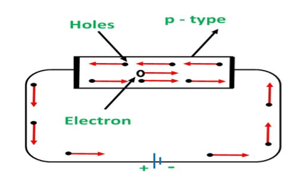
In p-type semiconductors, a large number of holes are created by the trivalent impurity. When a potential difference is applied across this type of semiconductors.
|
Figure 9: Conduction through p type semiconductor
The holes are available in the valence band are directed towards the negative terminal. As the current flow through the crystal is by holes, which are a carrier of positive charge, therefore, this type of conductivity is known as positive or p-type conductivity. In a p-type conductivity, the valence electrons move from one covalent to another.
The conductivity of an n-type semiconductor is nearly double that of a p-type semiconductor. The electrons available in the conduction band of the n-type semiconductor are much more movable than holes available in the valence band in a p-type semiconductor. The mobility of holes is poor as they are more bound to the nucleus.
Even at room temperature, the electron-hole pairs are formed. These free electrons which are available in minute quantity also carry a little amount of current in the p-type semiconductors.
N-TYPE EXTRINSIC SEMICONDUCTOR
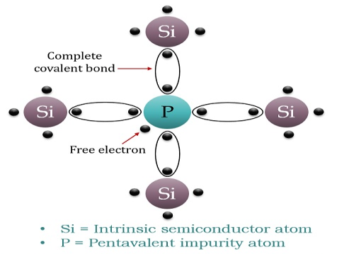
When a few Pentavalent impurities such as Phosphorus whose atomic number is 15, which is categorized as 2, 8, and 5. It has five valence electrons, which are added to silicon crystals. Each atom of the impurity fits in four silicon atoms as shown in the figure below.
Hence, each Arsenic atom provides one free electron in Silicon crystal. Since an extremely small amount of Phosphorus, impurity has a large number of atoms; it provides millions of free electrons for conduction.
|
Figure 10: N-type semiconductor
An N-type semiconductor material has an excess of electrons. In this way, free electrons are available within the lattices, and their overall movement in one direction under the influence of a potential difference results in an electric current flow. This is an N-type semiconductor, the charge carriers are electrons.
ENERGY DIAGRAM OF N-TYPE SEMICONDUCTOR
A large number of free electrons are available in the conduction band because of the addition of the Pentavalent impurity. These electrons are free electrons that did not fit in the covalent bonds of the crystal. However, a minute quantity of free electrons is available in the conduction band forming hole- electron pairs.
The Energy diagram of the n-type semiconductor is shown in the figure below.
|
Figure 11: Energy diagram of the n-type semiconductor
- The addition of pentavalent impurity results in a large number of free electrons.
- When thermal energy at room temperature is imparted to the semiconductor, a hole-electron pair is generated and as a result, a minute quantity of free electrons is available. These electrons leave behind holes in the valence band.
- Here n stands for negative material as the number of free electrons provided by the pentavalent impurity is greater than the number of holes.
CONDUCTION THROUGH N-TYPE SEMICONDUCTOR
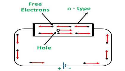
In the n-type semiconductor, a large number of free electrons are available in the conduction bands which are donated by the impurity atoms. The figure below shows the conduction process of an n-type semiconductor.
When a potential difference is applied across this type of semiconductor, the free electrons are directed towards the positive terminals. It carries an electric current. As the flow of current through the crystal is constituted by free electrons which are carriers of a negative charge, therefore, this type of conductivity is known as negative or n-type conductivity.
|
Figure 12: Conduction through n-type semiconductor
The electron-hole pairs are formed at room temperature. These holes which are available in small quantities in the valence band also consist of a small amount of current. For practical purposes, this current is neglected.
Key Takeaways
- The semiconductor is divided into two types. One is an Intrinsic Semiconductor and the other is an Extrinsic semiconductor.
- The pure form of the semiconductor is known as the intrinsic semiconductor
- The semiconductor in which intentional impurities are added for making it conductive is known as the extrinsic semiconductor.
- A hole is the absence of an electron in a particular place in an atom.
- The process by which an impurity is added to a semiconductor is known as Doping.
- Depending upon the type of impurity added the extrinsic semiconductor may be classified as an n-type semiconductor and p-type semiconductor.
- The extrinsic p-Type Semiconductor is formed when a trivalent impurity is added to a pure semiconductor in a small amount, and as a result, a large number of holes are created in it.
- The extrinsic n-Type Semiconductor is formed when a Pentavalent impurity is added to a pure semiconductor in a small amount, and as a result, a large number of electrons are created in it.
FERMI ENERGY Intrinsic semiconductors—carrier concentrationHere we will calculate the number of electrons excited into the conduction band at temperature T and also the hole concentration in the valence band. It is assumed that the electrons in the conduction band behave as if they are free particles with effective mass me* and the holes near the top of the valence band behave as if they are free particles with effective mass mh*. Here we will calculate the electron concentration, hole concentration The density of Electrons in Conduction Band The number of free electrons per unit volume of a semiconductor having energies in between E and E + dE is represented as N(E) dE dE = width of Energy band Therefore, we have: N(E) dE = ge(E) dE fe(E) ……….(1) ge(E) = The density of electron states per unit volume fe(E) = Fermi-Dirac distribution function i.e. probability that an electron occupies an electron state The number of electrons present in the conduction band per unit volume of material ‘n’ is obtained by integrating N(E) dE between the limits Ec and Ect Where Ec = the bottom energy levels of the conduction band Ect = the bottom and top energy levels of the conduction band n = can be written as n = n = we know that above Ect, there are no electrons. Hence, Equation (3) becomes n = n = The Fermi-Dirac distribution function fe(E) can be represented as:
Compared to the exponential value, so the ‘1’ in the denominator can be neglected. So Hence, The density of electron states ge(E) in the energy space from E = 0 to E can be written as:
where me* is the effective mass of an electron and h is Planck’s constant.
To evaluate n, the density of states is counted from Ec, since the minimum energy state in the conduction band is Ec. so eq (8) can become
Substituting Equations (6) and (9) in (4) gives n = n = The above equation can be simplified by the following substitution: Put ɛ = E − Ec ………… (11) So, dɛ = dE In Equation (11), Ec is constant, as we change the variable E to ε in Equation (10), the integral limits also change. In Equation (11), as E → Ec then ε → 0 and E → ∞, then ε also → ∞. the exponential term in Equation (10) becomes:
Substituting Equations (11) and (12) in (10), we get: n = n = Above integral (I) can be simplified by substitution. Put ε = x2 so that dɛ = 2x dx I = = = Substituting Equation (14) in (13) gives: n = n = n = n = The term n =Nc The density of Holes in Valence Band The number of holes per unit volume of semiconductor in the energy range E and E + dE in the valence band is represented as P(E) dE. Proceeding the same way (as in the case of electrons) we have Therefore, we have: P(E) dE = gh(E) dE fh(E) ……….(17) dE = width of Energy band gh(E) = The density of holes states per unit volume fh(E) = Fermi-Dirac distribution function i.e. probability that a hole occupies an electron state The number of electrons present in the conduction band per unit volume of material ‘n’ is obtained by integrating P(E) dE between the limits Evb and EV where EV = the bottom energy levels of the valence band Evb = the bottom and top energy levels of the valence band The total number of holes present in the valence band per unit volume of material ‘p’ is obtained by integrating P(E) dE
Equation (18) can be represented as:
Now we know that below Evb no holes are present. Hence, Equation (19) becomes
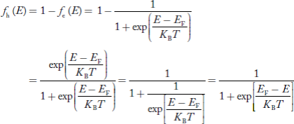
We know a hole can also be defined as the absence of an electron. presence of a hole = the absence of an electron Hence, the Fermi-Dirac function of holes fh(E) in the valence band is:
Compared to exponential, the ‘1’ in the denominator is negligible, Hence,
The density of hole states between E and E + dE in valence band can be written similar to Equation (8.9) for electrons.
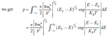
Where mh* is the effective mass of the hole. Substituting Equations (21) and (22) in (20),
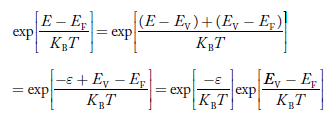
The above equation can be simplified by the substitution: Put ɛ = EV − E ............. (24) so dɛ = − dE In Equation (24), EV is constant, as we change the variable E to ε in Equation (23), the integral limits also change. In Equation (24), as E → EV then ε → 0 and E→ −∞, then ε → ∞ the exponential term in Equation (23) becomes:
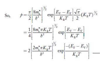
Substituting Equations (24) and (25) in (23), we get:
From Equation (14), we know the integral value
….The term
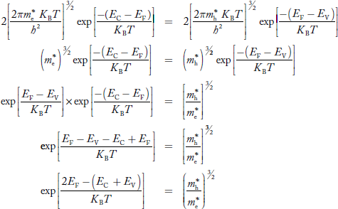
Fermi Level We know that in an intrinsic semiconductor Electron concentration ‘n’ = Hole concentration ‘p’ Equating Equations (15) and (27), we get
Taking logarithms on both sides, we get
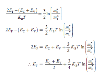
Normally, mh* is greater than me*, since ln Temperature effect on Fermi level Fermi level slightly rises with an increase of temperature. But in the case of a pure intrinsic semiconductor like Si and Ge, mh* ≈ me* So in these cases, the Fermi level lies in the middle of the energy gap. DEPENDENCE OF FERMI ENERGY ON CARRIER CONCENTRATION AND TEMPERATURE (QUALITATIVE)- Carrier Concentration in Extrinsic SemiconductorsThe number of charge carriers presents per unit volume of a semiconductor material is called carrier concentration. Suppose donor and acceptor atoms are doped in a semiconductor. At temperature T K, n = number of conduction electrons p = number of holes N−A = number of acceptor ions N+D = number of donor ions We know that the below equation holds good in the semiconductor. The total negative charge due to conduction electrons and acceptor ions is equal to holes and donor ions in a unit volume of material. So the material will be considered neutral if, n + N−A = p + N+D ……….(34) Equation (34) is called the charge neutrality equation. In the above equation
concentration of acceptor ions N−A = acceptor concentration x probability of finding an electron in acceptor level
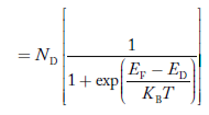
Similarly, the donor ions concentration is
In n-type material Note nn represents electrons in n-type material pn represents holes concentration in n-type material.
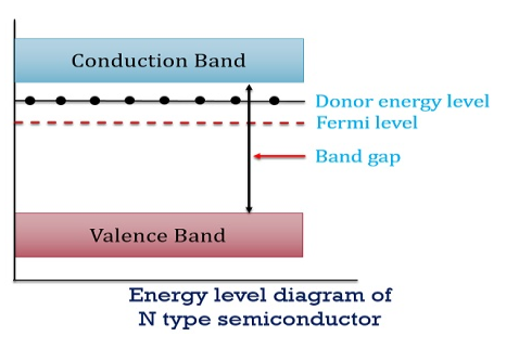
there are no acceptor atoms so N−A = 0. At 0 K, all the electron states at the donor level are occupied by electrons. As the temperature is increased from 0 K, some of the electrons jump from these donor states into the conduction band. Also, the concentration of holes is extremely less compared with the concentration of conduction electrons [p << n] From Equation (34) we have n = p N+D (Or) n ≈ N+D …………(38) [since p << N+D] At temperature T K, As the temperature increase, almost all the donor atoms donate electrons to the conduction band.
Figure 13: Energy level diagram of N type semiconductor
So, in n-type material, the free electron concentration is almost equal to the donor atoms. So we can rewrite the above equation as nn ≈ ND …………….(39) where nn represents electrons in n-type material also, the hole concentration in n-type material can be obtained by applying the law of mass action nn pn =ni2
where pn represents holes concentration in n-type material. In n-type material at 0 K, the Fermi energy level lies in the middle of Ec and ED
At temperature> 0K
With the increase in temperature, the Fermi level shifts upwards according to Equation (61) slightly due to the ionization of donor atoms. With further increase of temperature, electron-hole pairs are generated due to the breaking of covalent bonds, hence Fermi level shifts downwards. In p-type semiconductor Note pp represents holes in the p-type material np represents electrons in the p-type material There are no donor atoms so means no ions present At 0 K, all the acceptor levels are not occupied by electrons. As the temperature is increased from 0 K, some electrons jump from top valence band energy levels to the acceptor states, leaving holes in the valence band and acceptor ions At some room temperature T K, the concentration of conduction electrons is extremely less compared with hole concentration. ∴ From Equation (34), we have n + N−A = p ……………(42) (or) N−A ≈ p ……………. (43) [since n << N−A] At temperature T K, in p-type material, the hole concentration is almost equal to the acceptor atoms in a unit volume of the material. So, Equation (43) can be written as pp ≈ NA ……………….(44) where pp represents holes in the p-type material The electron concentration in p-type material can be obtained by applying the law of mass action as nppp = ni2
where np represents free electron concentration in the p-type material.
Figure 14: Energy level diagram of N type semiconductor. In p-type material, the Fermi level lies in between EV and EA at 0 K
As the temperature is increased from 0 K, the Fermi level shifts downwards slightly as per Equation (46) due to ionization of acceptor atoms. And with a further increase of temperature, electron-hole pairs are generated due to the breaking of covalent bonds, so the Fermi level shifts upwards. |
Key Takeaways
|
When the magnetic field is applied perpendicular to a current-carrying conductor, then a voltage is developed in the material perpendicular to both the magnetic field and current in the conductor. This effect is known as Hall Effect and the voltage developed is known as Hall voltage (VH).
Hall Effect is useful to identify the nature of charge carriers in material and hence to decide whether the material is an n-type semiconductor or p-type semiconductor, also to calculate carrier concentration and mobility of carriers.
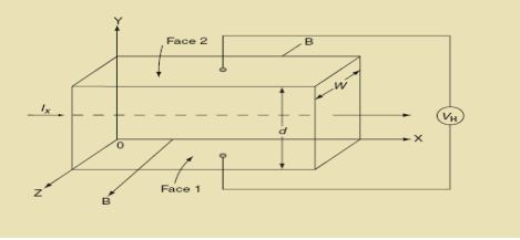
Hall Effect can be explained by considering a rectangular block of an extrinsic semiconductor in which current is flowing along the positive X-direction and magnetic field B is applied along Z-direction as shown in Figure.
|
Figure 15: Hall Effect
Suppose if the semiconductor is n-type, then mostly the carriers are electrons and the electric current is due to the drifting of electrons along negative X-direction or if the semiconductor is p-type, then mostly the carriers are holes and the electric current is due to drifting of the holes along positive X-direction.
As these carriers are moving in the magnetic field in the semiconductor that means they experience Lorentz force represented by FL
FL = Bevd
Where vd is the drift velocity of the carriers. (already explained in the previous section).
We can obtain the direction of this force by applying Fleming’s left-hand rule in electromagnetism.
Fleming’s left-hand rule can be explained as If we stretch the thumb, forefinger, and middle finger in three perpendicular directions so that the forefinger is parallel to the magnetic field and the middle finger is parallel to the current direction, then the thumb represents the direction of the force on the current-carrying carriers.
So the Lorentz force is exerted on the carriers in the negative Y-direction. Due to Lorentz force, more and more carriers will be deposited at the bottom face (represented by face 1in the figure) of the conductor.
The deposition of carriers at the bottom face is continued till the repulsive force due to accumulated charge balances the Lorentz force.
After some time of the applied voltage, both the forces become equal in magnitude and act in opposite direction, then the potential difference between the top and bottom faces is equal to Hall voltage and that can be measured.
At equilibrium, the Lorentz force on a carrier FL = Bevd ……………..(1) and the Hall force FH = eEH ……………..(2) Where EH is the Hall electric field due to accumulated charge. At equilibrium, FH = FL eEH = Bevd ∴ EH = Bvd ……………..(3) If ‘d’ is the distance between the upper and lower surfaces of the slab, then the Hall field EH = In n-type material, Jx = –nevd vd = - Where n is free electron concentration, substituting (5) in (3), we have ∴ EH = -B For a given semiconductor, the Hall field EH is proportional to the current density Jx and the intensity of magnetic field ‘B’ in the material. i.e. EH ∝ JxB (or) EH = RHJxB ……………..(7) Where RH = Hall coefficient Equations (6) and (7) are the same so, we have RHJxB =-B RH = - Where ρ is the charge density Similarly for p-type material RH = Using Equations (8) and (9), carrier concentration can be determined. Thus, the Hall coefficient is negative for n-type material. In n-type material, as the more negative charge is deposited at the bottom surface, so the top face acquires positive polarity and the Hall field is along negative Y-direction. The polarity at the top and bottom faces can be measured by applying probes. Similarly, in the case of p-type material, a more positive charge is deposited at the bottom surface. So, the top face acquires negative polarity and the Hall field is along positive Y-direction. Thus, the sign of the Hall coefficient decides the nature of (n-type or p-type) material. The Hall coefficient can be determined experimentally in the following way: Multiplying Equation (7) with ‘d’, we have EHd = VH = RHJxBd ……………..(10) From (Figure 15) we know the current density Jx Jx = Where W is the width of the box. Then, Equation (10) becomes VH = RH RH = Substituting the measured values of VH, Ix, B, and W in Equation(11), RH is obtained. The polarity of VH will be the opposite for n- and p-type semiconductors. The mobility of charge carriers can be found by using the Hall effect, for example, the conductivity of electrons is n = neμn Or we can rewrite it as μn = by using equation (11) μn = n |
• Using magnetic flux leakage – To properly inspect items such as pipes or tubes, Hall Effect probes work with something called magnetic flux leakage. This is a way of testing such items, and being able to spot potential corrosion, erosion, or pitting. This is specifically used in steel items and can give important information about lifespan or safety.
• Sensors to detect rotation speed – A Hall Effect probe can be used in bicycle wheels, speedometers in the automotive world, electronic types of ignition systems, and gear teeth.
• Used to detected movement – You will often find a Hall Effect probe used in such items as Go-Kart controls, smartphones, paintball guns, or airsoft guns, as well as some GPS systems.
• Ferrite Toroid Hall Effect current transducers – This is mainly used in electronic compasses, making use of the magnetic field to show direction.
• Split-ring clamp-on sensors – These types of Hall Effect probes are used to test equipment without having to take the whole circuit board apart, e.g. complex items.
• Analog multiplication – Anything which needs a power measurement, e.g. sensing, and is also used in small computers.
• General power measurement – Any device which needs to be tested for its power input can be done by a Hall Effect probe.
• Position and motion sensors – This is mainly used in a DC motor, often the brushless type.
• The automotive world – Hall Effect probes are used widely in the automotive world, especially in fuel injection and ignition. Wheel rotation sensors also use Hall Effect probes, e.g. for anti-lock braking.
- For determination of the type of given semiconductor.
- For N-type, Hall coefficient RH= negative
- For P-type, Hall coefficient RH= Positive
- To determine carrier concentration n and p; that is n=p=1/e𝑅𝐻
- Determination of mobility of charge carriers μn =
 =n RH. Where 𝜎= electrical conductivity
 - To determine the sign of charge carriers whether the conductivity is due to electrons or holes.
Main Advantages of Using Hall Sensors
Why is a Hall Effect probe advantageous in all of these instances? Because the probes are not affected by outside influences, e.g. water or dirt. They can also easily sense the measure of the output they need when they are placed in the right position. On top of this, Hall Effect probes are safer, because the voltage never actually makes it directly to the sensor/probe. This makes this type of measurement overall so much safer than other methods.
As you can see, understanding how something is put into practice in the real world helps you to understand it in real terms. The Hall Effect is certainly very commonplace these days, in much more methods and applications than we realize. While certainly very useful in the automation world, even basic items such as a compass make large use of this scientific approach.
Key Takeaways
- When the magnetic field is applied perpendicular to a current-carrying conductor, then a voltage is developed in the material perpendicular to both the magnetic field and current in the conductor. This effect is known as Hall Effect.
- The voltage developed is known as Hall voltage (VH).
- Hall Effect is useful to identify the nature of charge carriers in material and hence to decide whether the material is an n-type semiconductor or p-type semiconductor.
- Hall Effect also to calculate carrier concentration and mobility of carriers.
- Hall coefficient is given by RH = -
 = -
= -  Where ρ is the charge density
 - Hall coefficient is given by RH =

- Mobility of charge carriers can be found by using the Hall Effect μn = n

HEISENBERG’S UNCERTAINTY PRINCIPLE
According to classical physics, given the initial conditions and the forces acting on a system, the future behaviour (unique path) of this physical system can be determined exactly. That is if the initial coordinates , velocity
  , and all the forces acting on the particle are known, the position
  , and velocity
  are uniquely determined by means of Newton’s second law. So by Classical physics, it can be easily derived.
Does this hold for the microphysical world?
Since a particle is represented within the context of quantum mechanics by means of a wave function corresponding to the particle’s wave, and since wave functions cannot be localized, then a microscopic particle is somewhat spread over space and, unlike classical particles, cannot be localized in space. In addition, we have seen in the double-slit experiment that it is impossible to determine the slit that the electron went through without disturbing it. The classical concepts of the exact position, exact momentum, and unique path of a particle therefore make no sense at the microscopic scale. This is the essence of Heisenberg’s uncertainty principle.
In its original form, Heisenberg’s uncertainty principle states that: If the x-component of the momentum of a particle is measured with an uncertainty ∆px, then its x-position cannot, at the same time, be measured more accurately than ∆x = ℏ/(2∆px). The three-dimensional form of the uncertainty relations for position and momentum can be written as follows:
|
This principle indicates that, although it is possible to measure the momentum or position of a particle accurately, it is not possible to measure these two observables simultaneously to arbitrary accuracy. That is, we cannot localize a microscopic particle without giving to it a rather large momentum.
We cannot measure the position without disturbing it; there is no way to carry out such a measurement passively as it is bound to change the momentum.
To understand this, consider measuring the position of a macroscopic object (you can consider a car) and the position of a microscopic system (you can consider an electron in an atom). On the one hand, to locate the position of a macroscopic object, you need simply to observe it; the light that strikes it and gets reflected the detector (your eyes or a measuring device) can in no measurable way affect the motion of the object.
On the other hand, to measure the position of an electron in an atom, you must use radiation of very short wavelength (the size of the atom). The energy of this radiation is high enough to change tremendously the momentum of the electron; the mere observation of the electron affects its motion so much that it can knock it entirely out of its orbit.
It is therefore impossible to determine the position and the momentum simultaneously to arbitrary accuracy. If a particle were localized, its wave function would become zero everywhere else and its wave would then have a very short wavelength. According to de Broglie’s relation p = ℏ /λ,
Time Energy Uncertainty Relation
The momentum of this particle will be rather high. Formally, this means that if a particle is accurately localized (i.e., ∆x  0), there will be total uncertainty about its momentum (i.e., ∆px
  ∞).
∞).
Since all quantum phenomena are described by waves, we have no choice but to accept limits on our ability to measure simultaneously any two complementary variables.
Heisenberg’s uncertainty principle can be generalized to any pair of complementary, or canonically conjugate, dynamical variables: it is impossible to devise an experiment that can measure simultaneously two complementary variables to arbitrary accuracy. If this were ever achieved, the theory of quantum mechanics would collapse.
Energy and time, for instance, form a pair of complementary variables. Their simultaneous measurement must obey the time-energy uncertainty relation:
|
This relation states that if we make two measurements of the energy of a system and if these measurements are separated by a time interval ∆t, the measured energies will differ by an amount ∆E which can in no way be smaller than ℏ /∆t. If the time interval between the two measurements is large, the energy difference will be small. This can be attributed to the fact that, when the first measurement is carried out, the system becomes perturbed and it takes it a long time to return to its initial, unperturbed state. This expression is particularly useful in the study of decay processes, for it specifies the relationship between the mean lifetime and the energy width of the excited states.
In contrast to classical physics, quantum mechanics is a completely indeterministic theory. Asking about the position or momentum of an electron, one cannot get a definite answer; only a probabilistic answer is possible.
According to the uncertainty principle, if the position of a quantum system is well defined its momentum will be totally undefined. 1 Example: The uncertainty in the momentum of a ball traveling at 20m/s is 1×10⁻⁶ of its momentum. Calculate the uncertainty in position? The mass of the ball is given as 0.5kg. Solution: Given m = 0.5kg, h = 6.626 × 10⁻³⁴ m2 kg / s Δp =p×1×10⁻⁶ As we know that, Δp = 10-5 Heisenberg Uncertainty principle formula is given as, ∆x∆p ∆x ∆x ∆x =0.527 x 10⁻²⁹ m 2 Example: The mass of a ball is 0.15 kg & its uncertainty in position to 10–10m. What is the value of uncertainty in its velocity? Solution: Given m=0.15 kg. h=6.6×10⁻³⁴ Joule-Sec. Δx = 10 –10 m Δv=? Δx.Δv ≥h/4πm Δv≥h/4πmΔx ≥6.6×10⁻³⁴/4×3.14×0.15×10–10 ≥ 3.50×10⁻²⁴m |
APPLICATIONS OF HEISENBERG UNCERTAINTY PRINCIPLE
The Heisenberg uncertainty principle based on quantum physics explains several facts that could not be explained by classical physics.
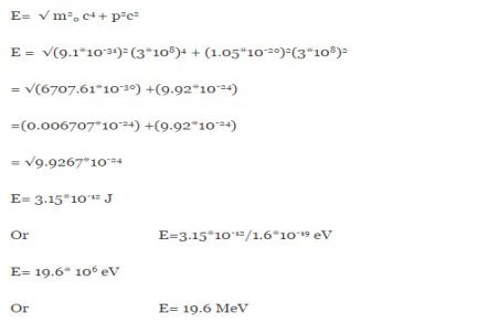
One of the applications is to prove that electrons cannot exist inside the nucleus. But to prove it, let us assume that electrons exist in the nucleus. As the radius of the nucleus is approximately 10-14m. If an electron is to exist inside the nucleus, then the uncertainty in the position of the electron is given by According to the uncertainty principle ∆x ∆p =h/2π Thus ∆p=h/2π∆x Or ∆p=6.62 x10⁻³⁴/2 x 3.14 x 10-14 Or ∆p=1.05 x 10⁻²⁰ kg m/ sec If this is p the uncertainty in the momentum of electron then the momentum of the electron should be at least of this order that is p=1.05*10-20 kg m/sec. An electron having this much high momentum must have a velocity comparable to the velocity of light. Thus, its energy should be calculated by the following relativistic formula E =
Therefore, if the electron exists in the nucleus, it should have an energy of the order of 19.6 MeV. However, it is observed that beta-particles (electrons) ejected from the nucleus during b – decay has energies of approximately 3 Me V, which is quite different from the calculated value of 19.6 MeV. Another reason that electrons cannot exist inside the nucleus is that experimental results show that no electron or particle in the atom possesses energy greater than 4 MeV. Therefore, it is confirmed that electrons do not exist inside the nucleus.
2. Calculation of zero-point energy The minimum energy of a system at o k (zero Kelvin) is called zero-point energy. Consider a particle that is confined to move under the influence of the potential of dimensions a. Since the particle may be present anywhere in these dimensions, so uncertainty in position ∆x = a/2 (half the diameter). According to the uncertainty principle ∆x∆px = ℏ/2 or Thus ∆px= ℏ /2∆x ∆px= ℏ /2a/2 = ℏ /a Uncertainty in the momentum of a particle along the x-axis is ∆px= ℏ /a Assuming the momentum of a particle to be at least equal to uncertainty in it, the lowest possible value of K.E. of the particle is given by K.E. = Where m is the mass of the particle. Energy even at O K is given by the above equation. This minimum energy is called the zero-point energy. This implies that even at zero kelvin, the particle is never at rest. If it is so, then ∆pX = 0, which is not possible. [It gives ∆x = ∞] 3. Existence of proton, neutron, and alpha particles within the nucleus. We know that the rest mass of the protons and neutron is of the order of 1.67x 10⁻²⁷ kg. Hence, the value of momentum 5.27 x 10⁻²¹ kg.m/sec from calculation and also the value of v come out to be 3x 10⁵m/sec.
The corresponding value of kinetic energy of a neutron or a proton is E =
Since the rest mass of the a-particle is nearly four times the proton mass, therefore the alpha particle should have a minimum kinetic energy of one-fourth of 52.05 keV or about 13 keV. Since the energy carried by the protons or neutrons emitted by the nuclei is greater than 52 keV and for a-particle of more than 13 keV, these particles can exist in the nuclei.
4. Size of Elementary cell in Phase space We have studied in our previous class that the state of a microsystem is defined by six variables – three are due to position and three due to momentum.
Hence, a system of N particles needs 6 N variables If ∆ x and ∆px be the uncertainly in position and momentum measurements then ∆ x ∆ px =
Similarly ∆ y ∆ py =
And ∆ z ∆ pz =
Multiplying these three equations, we get ∆ x ∆ y ∆ z ∆ px ∆ py ∆ pz = ( The above product is called the volume of elementary cells in phase space. So, the volume of an elementary cell in phase space
5. Accurate limit of frequency of radiation emitted by an atom Consider the radiation emitted from an excited atom. The energy of this atom will decrease when it emits one or more photons of characteristic frequency. The average period between excitation of the atom and the release of energy is about 10-8 seconds.
Thus, uncertainly in energy is ∆ E
Or ∆ E
Or ∆ E
The frequency of light is uncertain by
∆ ν = As a result, the radiation from an excited atom does not have the noted precise frequency new ν - ∆ ν and ν + ∆ ν. |
Key Takeaways
2. The three-dimensional form of the uncertainty relations for position and momentum can be written as follows:
3. Energy and time, for instance, form a pair of complementary variables. Their simultaneous measurement must obey the time-energy uncertainty relation:
|
Schrodinger wave equation is the fundamental equation of quantum mechanics, the same as the second law of motion is the fundamental equation of classical mechanics. This equation has been derived by Schrodinger in 1925 using the concept of the wave function based on de-Broglie wave and plank’s quantum theory. Let us consider a particle of mass m and classically the energy of a particle is the sum of the kinetic and potential energies. We will assume that the potential is a function of the only x. So We have E= K+V =
By de Broglie’s relation, we know that all particles can be represented as waves with frequency ω and wavenumber k and that E= ℏω and p= ℏk. Using this equation (1) for the energy will become ℏω =
A wave with frequency ω and wavenumber k can be written as usual as ψ(x, t) =Aei(kx−ωt) ……….. (3)
the above equation is for one dimensional and three dimensional we can write it as ψ(r, t) =Aei(k·r−ωt) ……….. (4) But here we will stick to one dimension only.
If we multiply the energy equation in Eq. (2) by ψ and using(5) and (6), we obtain ℏ(ωψ) = This is the time-dependent Schrodinger equation. If we put the x and t in the above equation then equation (7) takes the form as given below
In 3-D, the x dependence turns into dependence on all three coordinates (x, y, z) and the
The term |ψ(x)|2 gives the probability of finding the particle at position x.
Let us again take it as simply a mathematical equation, then it’s just another wave equation. However, We already know the solution as we used this function ψ(x, t) =Aei(kx−ωt) to produce Equations (5), (6), and (7)
But let’s pretend that we don’t know this, and let’s solve the Schrodinger equation as if we were given to us. As always, we will guess an exponential solution by looking at exponential behaviour in the time coordinate, our guess is ψ(x, t) =e−iωtf(x) putting this into Equation (7) and canceling the e−iωt yields
We already know that E=
Eψ = -
This is called the time-independent Schrodinger equation.
|
Key Takeaways
1. Schrodinger wave equation is the fundamental equation of quantum mechanics, the same as the second law of motion is the fundamental equation of classical mechanics. 2. The time-dependent Schrodinger equation.
3. The term |ψ(x)|2 gives the probability of finding the particle at position x. 4. The time-independent Schrodinger equation.
Eψ = - |
The wave function, at a particular time, contains all the information that anybody at that time can have about the particle. But the wave function itself has no physical interpretation. It is not measurable. However, the square of the absolute value of the wave function has a physical interpretation. We interpret |ψ(x,t)|2 as a probability density, a probability per unit length of finding the particle at a time t at position x.
The wave function ψ associated with a moving particle is not an observable quantity and does not have any direct physical meaning. It is a complex quantity. The complex wave function can be represented as ψ(x, y, z, t) = a + ib and its complex conjugate as ψ*(x, y, z, t) = a – ib. The product of wave function and its complex conjugate is ψ(x, y, z, t)ψ*(x, y, z, t) = (a + ib) (a – ib) = a2 + b2 a2 + b2 is a real quantity.
However, this can represent the probability density of locating the particle at a place in a given instant of time.
The positive square root of ψ(x, y, z, t) ψ*(x, y, z, t) is represented as |ψ(x, y, z, t)|, called the modulus of ψ. The quantity |ψ(x, y, z, t)|2 is called the probability. This interpretation is possible because the product of a complex number with its complex conjugate is a real, non-negative number.
We should be able to find the particle somewhere, we should only find it at one place at a particular instant, and the total probability of finding it anywhere should be one.
For the probability interpretation to make sense, the wave function must satisfy certain conditions.
Only the wave function with all these properties can yield a physically meaningful result.
The physical significance of wave function
The Schrodinger equation is also known as Schrodinger’s wave equation is a partial differential equation that describes the dynamics of quantum mechanical systems by the wave function. The trajectory, the positioning, and the energy of these systems can be retrieved by solving the Schrodinger equation. All of the information for a subatomic particle is encoded within a wave function. The wave function will satisfy and can be solved by using the Schrodinger equation. The Schrodinger equation is one of the fundamental axioms that are introduced in undergraduate physics. |
Key Takeaways
|
It is well known that an atom can be characterized by a unique set of discrete energy states. When excited through heating or electron bombardment in a discharge tube, the atom makes transitions between these quantized energy states and emits light. The emitted light forms a discrete spectrum, reflecting the quantized nature of the energy states or energy levels. In the presence of a magnetic field, these energy levels can shift. This effect is known as the Zeeman effect.
The origin of the Zeeman Effect
In an atomic energy state, an electron orbits around the nucleus of the atom and has a magnetic dipole moment associated with its angular momentum. In a magnetic field, it acquires additional energy just as a bar magnet does, and consequently, the original energy level is shifted. The energy shift may be positive, zero, or even negative, depending on the angle between the electron magnetic dipole moment and the field. Due to the Zeeman effect, some degenerate energy levels will split into several non-degenerate energy levels with different energies. This allows for new transitions which can be observed as new spectral lines in the atomic spectrum.
For singlet states, the spin is zero and the total angular momentum J is equal to the orbital angular momentum L. When placed in an external magnetic field, the energy of the atom changes because of the energy of its magnetic moment in the field, which is given by
where the z-direction is defined by the direction of B. we have μz =- μB Ml = - The classical theory accounts for only one type of angular momentum called orbital angular momentum. The Hamiltonian for an electron with angular momentum
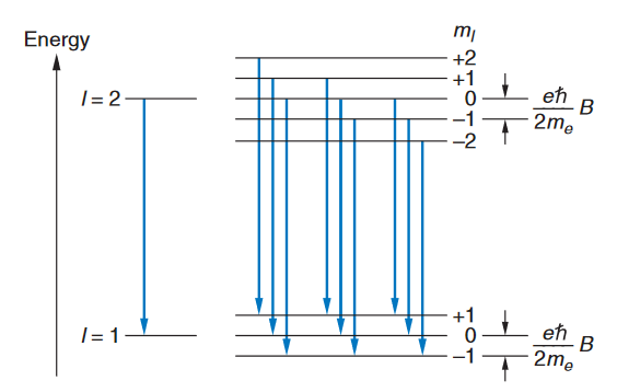
where Ml is the quantum number for the component of Since there are 2l+1 values of Ml, each energy level splits into 2l+1 levels. Figure 16 shows the splitting of the levels for the case of a transition between a state with l=2 and one with l=1. The selection rule Ml ={1 restricts the number of possible lines to the nine shown. Because of the uniform splitting of the levels, there are only three different transition energies. Corresponding to the transitions with Ml =+1, Ml =0, and Ml =-1. We can see that there will only be these energies for any initial and final values of l.
FIGURE 16: Energy-level splitting in the normal Zeeman effect for singlet levels l=2 and l=1. Each level is split into 2l+1 terms. The nine transitions consistent with the selection rule But electrons also have a different type of angular momentum called intrinsic spin angular momentum,
The shift is analogous to that due to orbital angular momentum, except for the constant factor of gs. The energy shift for a particular state depends only on Ms (Ml for the orbital case) for that state. If an atom had only a single electron and the electron had only "intrinsic spin" angular momentum, then Equation 2 would represent the Zeeman shift. Atoms typically have many electrons and are characterized by a total angular momentum
where g, called the Landé g factor, is given by
The important difference is that g depends on the particular state of interest, as does MJ.
|
Key Takeaways
- It is well known that an atom can be characterized by a unique set of discrete energy states. In the presence of a magnetic field, these energy levels can shift. This effect is known as the Zeeman Effect.
- When placed in an external magnetic field, the energy of the atom changes because of the energy of its magnetic moment in the field, which is given by
 E = -μ .B = -μz .B where μz =- μB Ml = -
  Ml
Ml
3. Energy levels are shifted by
 E = μB Ml H
The phenomenon of Raman scattering of light was experimentally observed in 1928 by Raman and Krishnan. Raman scattering is most easily seen as the change in frequency for a small percentage of the intensity in a monochromatic beam as the result of coupling between the incident radiation and vibrational energy levels of molecules. A vibrational mode will be Raman active only when it changes the polarizability of the molecule.
Introduction
When monochromatic radiation with a wavenumber ν0 is incident on systems, most of it is transmitted without change, but, in addition, some scattering of the radiation occurs. If the frequency content of the scattered radiation is analyzed, there will be observed to be present not only the wavenumber ν0 associated with the incident radiation but also, in general, pairs of new wavenumbers of the type ν′= ν0+ νM.
In molecular systems, the wavenumbers νM are found to lie principally in the ranges associated with transitions between rotational, vibrational, and electronic levels. Such scattering of radiation with the change of wavenumber is called Raman Scattering, after the Indian scientist C. V. Raman who, with K. S. Krishnan, first observed this phenomenon in liquids in 1928.
Due to its very low scattering efficiency, Raman spectroscopy did not become popular until powerful laser systems were available after the 1960s. Now, Raman spectroscopy has become one of the most popular approaches to study the vibrational structures of molecules together with the infrared spectrum.
The origin of the modified frequencies found in Raman scattering is explained in terms of energy transfer between the scattering system and the incident radiation. When a system interacts with radiation of wavenumber ν0, it makes an upward transition from a lower energy level E1 to an upper energy level E2. It must then acquire the necessary energy, ΔE= E2- E1, from the incident radiation. The energy ΔE is expressed in terms of a wavenumber νM associated with the two levels involved, where
ΔE=hcνM …………. (1)
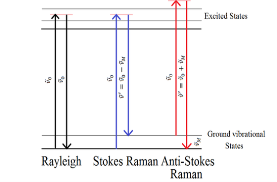
This energy requirement is regarded as being provided by the absorption of one photon of the incident radiation of energy hcν0 and the simultaneous emission of a photon of smaller energy hc(ν0 - νM), so that scattering of radiation of lower wavenumber, ν0 - νM, occurs.
Alternatively, the interaction of the radiation with the system may cause a downward transition from a higher energy level E2 to a lower energy level E1, in which case it makes available energy
E2−E1=hcνM …………. (2)
Again a photon of the incident radiation of energy hcν0 and the simultaneous emission of a photon of higher energy hc(ν0 + νM), so that scattering of radiation of higher wavenumber, ν0 + νM, occurs.
In the case of Rayleigh scattering, although there is no resultant change in the energy state of the system, the system still participates directly in the scattering act, causing one photon of incident radiation hcν0 to be absorbed and a photon of the same energy to be emitted simultaneously, so that scattering of radiation of unchanged wavenumber, ν0, occurs.
It is clear that, as far as wavenumber is concerned, a Raman band is to be characterized not by its absolute wavenumber but by the magnitude of its wavenumber shift νM from the incident wavenumber. Such wavenumber shifts are often referred to as Raman wavenumbers.
Where it is necessary to distinguish Stokes and anti-Stokes Raman scattering we shall define Δν to be positive for Stokes scattering and negative for anti-Stokes scattering, that is Δν= ν0+ν′
|
Figure 17: Diagrammatic representation of an energy transfer model of Rayleigh scattering, Stokes Raman, and anti-Stokes Raman scattering.
The intensity of anti-Stokes relative to Stokes Raman scattering decreases rapidly with an increase in the wavenumber shift. This is because anti-Stokes Raman scattering involves transitions to a lower energy state from a populated higher energy state.
The classical approach to the Raman Effect
Now we will explore the classical nature of the Raman effect. The classical theory of the Raman effect is based upon the polarizability of molecules, which reflects how easily an electron cloud of a molecule can be distorted by an electric field (light).
The technique is based on molecular deformations in electric field E determined by molecular polarizability α. The laser beam can be considered as an oscillating electromagnetic wave with electrical vector E. Upon interaction with the sample, it induces electric dipole moment P = αE which deforms molecules. Because of periodical deformation, molecules start vibrating with a characteristic frequency.
The scattered light can have a frequency equal to the incident light (Rayleigh), equal to the incident light minus the vibrational frequency (Stokes), and equal to the incident light plus the vibrational frequency (anti-Stokes).
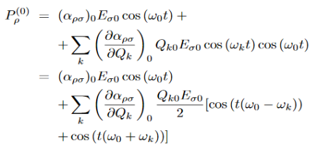
When a photon interacts with a molecule it will cause the electrons and protons to move and this will induce an oscillating dipole. This dipole will then radiate photons of different frequencies. To find these frequencies we start with a photon with the following electric field:
The induced dipole will then look like:
Where αρσ is the polarizability tensor of the molecule. This is a measure of how easy it is to polarize the molecule in each direction. This α does not have a constant value, it depends on the shape of the molecule. For small displacements the polarizability tensor can be expanded as a Taylor series in the normal coordinates of the molecule:
Where (αρσ)0 is the polarizability tensor at the equilibrium configuration and Qk is the kth normal mode coordinate of the molecule associated with the vibrational frequency ωk. Since the normal modes are harmonic Q can be written as:
Plugging this into equation (3) and placing that into equation (2) will give the linear induced dipole vector
…………. (5) This clearly shows that the dipole contains three frequencies ω0, ω0 - ωk, and ω0+ωk. These give rise to Rayleigh, Stokes, and anti-Stokes scattering respectively.
|
Key Takeaways
- Raman scattering is most easily seen as the change in frequency for a small percentage of the intensity in a monochromatic beam as the result of coupling between the incident radiation and vibrational energy levels of molecules.
- When monochromatic radiation with a wavenumber ν0 is incident on systems, most of it is transmitted without change, but, in addition, some scattering of the radiation occurs.
- For Stokes scattering, Raman shift is given by Δν= ν0 - νM
- For anti-Stokes scattering, Raman shift is given by Δν= ν0+ν′
Reference Books
I. Engineering physics- Gaur and Gupta, & S.Chand Publication
2. Engineering physics - Avadhanalu and Kshirsagar, S.Chand Publication
3. Introduction to Solid State Physics -- Charles Kittel
4. Solid State Physics -- S.O.Pillai
5. Fundamentals of Molecular Spectroscopy -- Colin N.Banwell + Elaine M.MaCash
6. Introduction to Atomic Spectra -- Harvey Elliott White
7. Engineering physics- Hitendra K Malik, A.K.Singh, Tata McGraw Hill Education Private Limited, New Delhi
8. Modern Physics B.I.Theraja S. Chand and Company Ltd., Ram Nagar. New Delhi.
UNIT 4
SEMICONDUCTORS AND MODERN PHYSICS
Semiconductors
Semiconductors are materials that have a conductivity between conductors and insulators.
Semiconductors can be pure elements, such as silicon or germanium, or compounds such as gallium arsenide or cadmium selenide.
They are not good conductors nor good insulators as their name “semi”-conductors.
These materials such as silicon (Si), germanium (Ge), and gallium arsenide (GaAs), have electrical properties somewhere in the middle, between those of a “conductor” and an “insulator”.
They have very few “free electrons” because their atoms are closely grouped in a crystalline pattern called a “crystal lattice” but electrons are still able to flow, but only under special conditions.
The Band Model
Bands are formed by the closely spaced orbitals.
There are three types of bands:
1. Valance Bands: A valence band is a group of orbitals that contain electrons in the shell. Or we can say It is also defined as the energy band that comprises of valence electrons present in the outermost shell of an atomic structure.
These valence electrons, when provided with sufficient energy, get changed into free electrons and moves to the conduction band thereby causing conductivity. It is at a lower energy level than the conduction band in the energy level diagram.
2. Conduction Band: A conduction band is a group of empty orbitals of the shells that do not contain any electron due to their configuration making the orbitals of higher energy levels.
When the electrons pass from the valance band to the conduction band these solids conduct electricity with the flow of charges in the form of electrons.
3. Forbidden Energy Band: These two bands are separated by a certain amount of energy known as the forbidden energy gap. In this band not a single electron is available. Its diagram is named Band Gap.
Let us distinguish between conductors, semiconductors, and insulators based on these bands.
|
Figure 1: Conductors, Semiconductors, and Insulators based on these bands.
- In Conductors: The valance band and the conduction band overlap each other. This makes it easy for electricity to pass through them. In conductors, the valence band is either not fully occupied with electrons, or the filled valence band overlaps with the empty conduction band. In general, both states occur at the same time, the electrons can therefore move inside the partially filled valence band or inside the two overlapping bands. In conductors, there is no bandgap between the valence band and conduction band.
- In Semi-conductors: there is a slight gap between the conduction band and the valance band. This bandgap is less than or equal to 1.4 eV. The electrons from the valance shell take a little energy to excite from the valance band to the conduction band. Even in semiconductors, there is a bandgap, but compared to insulators it is so small that even at room temperature electrons from the valence band can be lifted into the conduction band. The electrons can move freely and act as charge carriers.
- In Insulators: In insulators, the valence band is fully occupied with electrons due to the covalent bonds. To achieve conductivity, electrons from the valence band have to move into the conduction band. the energy gap is considerably large and the electrons of the valance band cannot be excited to the conduction band before the melting or the dissociation of the solid. This means that under the practically ambient condition it cannot conduct electricity.
Consider an isolated silicon atom; its energy levels are quantized. When two identical atoms are brought closer together, the quantized energy levels hybridize and split into two different levels because of the mutual interaction of the two atoms. More generally, when N atoms are moved closer until they reach the equilibrium inter-atomic distance d, the energy levels split into N levels. These N levels are very close to each other if N is large (which is the case in a crystal) so that they eventually form a continuous energy band.
|
Figure 2: Formation of Energy band as a function of interatomic distance (distance between atoms)
Key Takeaways
- Semiconductors are materials that have conductivity between conductors and insulators.
- Bands are formed by the closely spaced orbitals.
- There are three types of bands: Valence band, conduction band, Forbidden Energy Band
- On the basis of band theory we can classify the materials as conductors, semiconductors, and insulators based on these bands.
There are two basic groups or classifications that can be used to define the different semiconductor types:
- Intrinsic Semiconductor
- Extrinsic Semiconductor
|
Figure 3: Type of semiconductor
The semiconductor is divided into two types. One is an Intrinsic Semiconductor and the other is an Extrinsic semiconductor. The pure form of the semiconductor is known as the intrinsic semiconductor and the semiconductor in which intentional impurities are added for making it conductive is known as the extrinsic semiconductor.
The conductivity of the intrinsic semiconductor becomes zero at room temperature while the extrinsic semiconductor is very little conductive at room temperature. The detailed explanation of the two types of the semiconductor is given below.
INTRINSIC SEMICONDUCTOR
An intrinsic type of semiconductor material made to be very pure chemically. As a result, it possesses a very low conductivity level having very few charge carriers, namely holes and electrons, which it possesses in equal quantities.
|
Figure 4: Intrinsic Semiconductor
The most commonly used semiconductor basics material by far is silicon. Silicon has four valence electrons in its outermost shell which it shares with its neighbouring silicon atoms to form a full orbital of eight electrons. The structure of the bond between the two silicon atoms is such that each atom shares one electron with its neighbour making the bond very stable.
As there are very few free electrons available to move around the silicon crystal, crystals of pure silicon (or germanium) are therefore good insulators. Silicon atoms are arranged in a definite symmetrical pattern making them a crystalline solid structure. A crystal of pure silica (silicon dioxide or glass) is generally said to be an intrinsic crystal (it has no impurities) and therefore has no free electrons.
An extremely pure semiconductor is called an Intrinsic Semiconductor. Based on the energy band phenomenon, an intrinsic semiconductor at absolute zero temperature is shown below.
|
Figure 5: Intrinsic semiconductor at absolute zero temperature.
Its valence band is filled and the conduction band is empty. When the temperature is raised and some heat energy is supplied to it, some of the valence electrons are lifted to the conduction band leaving behind holes in the valence band as shown below.
|
Figure 6: Intrinsic semiconductor at T >0
A hole is the absence of an electron in a particular place in an atom. Although it is not a physical particle in the same sense as an electron, a hole can be passed from atom to atom in a semiconductor material. It is considered to have a positive charge. Holes are positive charge carriers.
The electrons reaching the conduction band move randomly. The holes created in the crystal also free to move anywhere.
This behaviour of the semiconductor shows that they have a negative temperature coefficient of resistance. This means that with the increase in temperature, the resistivity of the material decreases, and the conductivity increases.
But simply connecting a silicon crystal to a battery supply is not enough to extract an electric current from it. To do that we need to create a “positive” and a “negative” pole within the silicon allowing electrons and therefore electric current to flow out of the silicon. These poles are created by doping the silicon with certain impurities.
The process by which an impurity is added to a semiconductor is known as Doping. The amount and type of impurity which is to be added to the material have to be closely controlled during the preparation of extrinsic semiconductor. Generally, one impurity atom is added to 108 atoms of a semiconductor.
The purpose of adding impurity in the semiconductor crystal is to increase the number of free electrons or holes to make it conductive.
If a Pentavalent impurity, having five valence electrons is added to a pure semiconductor a large number of free electrons will exist. Which makes an n-type extrinsic semiconductor.
If a trivalent impurity having three valence electrons is added, a large number of holes will exist in the semiconductor. Which makes a p-type extrinsic semiconductor.
EXTRINSIC SEMICONDUCTOR
Extrinsic types of semiconductors are those where a small amount of impurity has been added to the basic intrinsic material. This 'doping' uses an element from a different periodic table group and in this way, it will either have more or fewer electrons in the valence band than the semiconductor itself. This creates either an excess or shortage of electrons. In this way two types of semiconductors are available: Electrons are negatively charged carriers. Holes are positively charged carriers.
Depending upon the type of impurity added the extrinsic semiconductor may be classified as an n-type semiconductor and p-type semiconductor.
P-TYPE EXTRINSIC SEMICONDUCTOR
The extrinsic p-Type Semiconductor is formed when a trivalent impurity is added to a pure semiconductor in a small amount, and as a result, a large number of holes are created in it. A large number of holes are provided in the semiconductor material by the addition of trivalent impurities like Gallium and Indium. Such type of impurities which produce a p-type semiconductor is known as an Acceptor Impurities because each atom of them creates one hole which can accept one electron.
In a P-type semiconductor material, there is a shortage of electrons, i.e. there are 'holes' in the crystal lattice. Electrons may move from one empty position to another and in this case, it can be considered that the holes are moving. This can happen under the influence of a potential difference and the holes can be seen to flow in one direction resulting in an electric current flow. It is harder for holes to move than for free electrons to move and therefore the mobility of holes is less than that of free electrons. Holes are positively charged carriers.
A trivalent impurity like Aluminium, having three valence electrons is added to Silicon crystal in a small amount. Each atom of the impurity fits in the Silicon crystal in such a way that its three valence electrons form covalent bonds with the three surrounding Silicon atoms as shown in the figure below.
|
Figure 7: p-Type Semiconductor
ENERGY BAND DIAGRAM OF P-TYPE SEMICONDUCTOR
The energy band diagram of a p-Type Semiconductor is shown below.
|
Figure 8: Energy band diagram of a p-Type Semiconductor
A large number of holes or vacant space in the covalent bond is created in the crystal with the addition of the trivalent impurity. A small or minute quantity of free electrons is also available in the conduction band.
They are produced when thermal energy at room temperature is imparted to the Silicon crystal-forming electron-hole pairs. But the holes are more in number as compared to the electrons in the conduction band. It is because of the predominance of holes over electrons that the material is called a p-type semiconductor. The word “p” stands for positive material.
CONDUCTION THROUGH P TYPE SEMICONDUCTOR
In p-type semiconductors, a large number of holes are created by the trivalent impurity. When a potential difference is applied across this type of semiconductors.
|
Figure 9: Conduction through p type semiconductor
The holes are available in the valence band are directed towards the negative terminal. As the current flow through the crystal is by holes, which are a carrier of positive charge, therefore, this type of conductivity is known as positive or p-type conductivity. In a p-type conductivity, the valence electrons move from one covalent to another.
The conductivity of an n-type semiconductor is nearly double that of a p-type semiconductor. The electrons available in the conduction band of the n-type semiconductor are much more movable than holes available in the valence band in a p-type semiconductor. The mobility of holes is poor as they are more bound to the nucleus.
Even at room temperature, the electron-hole pairs are formed. These free electrons which are available in minute quantity also carry a little amount of current in the p-type semiconductors.
N-TYPE EXTRINSIC SEMICONDUCTOR
When a few Pentavalent impurities such as Phosphorus whose atomic number is 15, which is categorized as 2, 8, and 5. It has five valence electrons, which are added to silicon crystals. Each atom of the impurity fits in four silicon atoms as shown in the figure below.
Hence, each Arsenic atom provides one free electron in Silicon crystal. Since an extremely small amount of Phosphorus, impurity has a large number of atoms; it provides millions of free electrons for conduction.
|
Figure 10: N-type semiconductor
An N-type semiconductor material has an excess of electrons. In this way, free electrons are available within the lattices, and their overall movement in one direction under the influence of a potential difference results in an electric current flow. This is an N-type semiconductor, the charge carriers are electrons.
ENERGY DIAGRAM OF N-TYPE SEMICONDUCTOR
A large number of free electrons are available in the conduction band because of the addition of the Pentavalent impurity. These electrons are free electrons that did not fit in the covalent bonds of the crystal. However, a minute quantity of free electrons is available in the conduction band forming hole- electron pairs.
The Energy diagram of the n-type semiconductor is shown in the figure below.
|
Figure 11: Energy diagram of the n-type semiconductor
- The addition of pentavalent impurity results in a large number of free electrons.
- When thermal energy at room temperature is imparted to the semiconductor, a hole-electron pair is generated and as a result, a minute quantity of free electrons is available. These electrons leave behind holes in the valence band.
- Here n stands for negative material as the number of free electrons provided by the pentavalent impurity is greater than the number of holes.
CONDUCTION THROUGH N-TYPE SEMICONDUCTOR
In the n-type semiconductor, a large number of free electrons are available in the conduction bands which are donated by the impurity atoms. The figure below shows the conduction process of an n-type semiconductor.
When a potential difference is applied across this type of semiconductor, the free electrons are directed towards the positive terminals. It carries an electric current. As the flow of current through the crystal is constituted by free electrons which are carriers of a negative charge, therefore, this type of conductivity is known as negative or n-type conductivity.
|
Figure 12: Conduction through n-type semiconductor
The electron-hole pairs are formed at room temperature. These holes which are available in small quantities in the valence band also consist of a small amount of current. For practical purposes, this current is neglected.
Key Takeaways
- The semiconductor is divided into two types. One is an Intrinsic Semiconductor and the other is an Extrinsic semiconductor.
- The pure form of the semiconductor is known as the intrinsic semiconductor
- The semiconductor in which intentional impurities are added for making it conductive is known as the extrinsic semiconductor.
- A hole is the absence of an electron in a particular place in an atom.
- The process by which an impurity is added to a semiconductor is known as Doping.
- Depending upon the type of impurity added the extrinsic semiconductor may be classified as an n-type semiconductor and p-type semiconductor.
- The extrinsic p-Type Semiconductor is formed when a trivalent impurity is added to a pure semiconductor in a small amount, and as a result, a large number of holes are created in it.
- The extrinsic n-Type Semiconductor is formed when a Pentavalent impurity is added to a pure semiconductor in a small amount, and as a result, a large number of electrons are created in it.
FERMI ENERGY Intrinsic semiconductors—carrier concentrationHere we will calculate the number of electrons excited into the conduction band at temperature T and also the hole concentration in the valence band. It is assumed that the electrons in the conduction band behave as if they are free particles with effective mass me* and the holes near the top of the valence band behave as if they are free particles with effective mass mh*. Here we will calculate the electron concentration, hole concentration The density of Electrons in Conduction Band The number of free electrons per unit volume of a semiconductor having energies in between E and E + dE is represented as N(E) dE dE = width of Energy band Therefore, we have: N(E) dE = ge(E) dE fe(E) ……….(1) ge(E) = The density of electron states per unit volume fe(E) = Fermi-Dirac distribution function i.e. probability that an electron occupies an electron state The number of electrons present in the conduction band per unit volume of material ‘n’ is obtained by integrating N(E) dE between the limits Ec and Ect Where Ec = the bottom energy levels of the conduction band Ect = the bottom and top energy levels of the conduction band n = can be written as n = n = we know that above Ect, there are no electrons. Hence, Equation (3) becomes n = n = The Fermi-Dirac distribution function fe(E) can be represented as:
Compared to the exponential value, so the ‘1’ in the denominator can be neglected. So Hence, The density of electron states ge(E) in the energy space from E = 0 to E can be written as:
where me* is the effective mass of an electron and h is Planck’s constant.
To evaluate n, the density of states is counted from Ec, since the minimum energy state in the conduction band is Ec. so eq (8) can become
Substituting Equations (6) and (9) in (4) gives n = n = The above equation can be simplified by the following substitution: Put ɛ = E − Ec ………… (11) So, dɛ = dE In Equation (11), Ec is constant, as we change the variable E to ε in Equation (10), the integral limits also change. In Equation (11), as E → Ec then ε → 0 and E → ∞, then ε also → ∞. the exponential term in Equation (10) becomes:
Substituting Equations (11) and (12) in (10), we get: n = n = Above integral (I) can be simplified by substitution. Put ε = x2 so that dɛ = 2x dx I = = = Substituting Equation (14) in (13) gives: n = n = n = n = The term n =Nc The density of Holes in Valence Band The number of holes per unit volume of semiconductor in the energy range E and E + dE in the valence band is represented as P(E) dE. Proceeding the same way (as in the case of electrons) we have Therefore, we have: P(E) dE = gh(E) dE fh(E) ……….(17) dE = width of Energy band gh(E) = The density of holes states per unit volume fh(E) = Fermi-Dirac distribution function i.e. probability that a hole occupies an electron state The number of electrons present in the conduction band per unit volume of material ‘n’ is obtained by integrating P(E) dE between the limits Evb and EV where EV = the bottom energy levels of the valence band Evb = the bottom and top energy levels of the valence band The total number of holes present in the valence band per unit volume of material ‘p’ is obtained by integrating P(E) dE
Equation (18) can be represented as:
Now we know that below Evb no holes are present. Hence, Equation (19) becomes
We know a hole can also be defined as the absence of an electron. presence of a hole = the absence of an electron Hence, the Fermi-Dirac function of holes fh(E) in the valence band is:
Compared to exponential, the ‘1’ in the denominator is negligible, Hence,
The density of hole states between E and E + dE in valence band can be written similar to Equation (8.9) for electrons.
Where mh* is the effective mass of the hole. Substituting Equations (21) and (22) in (20),
The above equation can be simplified by the substitution: Put ɛ = EV − E ............. (24) so dɛ = − dE In Equation (24), EV is constant, as we change the variable E to ε in Equation (23), the integral limits also change. In Equation (24), as E → EV then ε → 0 and E→ −∞, then ε → ∞ the exponential term in Equation (23) becomes:
Substituting Equations (24) and (25) in (23), we get:
From Equation (14), we know the integral value
….The term
Fermi Level We know that in an intrinsic semiconductor Electron concentration ‘n’ = Hole concentration ‘p’ Equating Equations (15) and (27), we get
Taking logarithms on both sides, we get
Normally, mh* is greater than me*, since ln Temperature effect on Fermi level Fermi level slightly rises with an increase of temperature. But in the case of a pure intrinsic semiconductor like Si and Ge, mh* ≈ me* So in these cases, the Fermi level lies in the middle of the energy gap. DEPENDENCE OF FERMI ENERGY ON CARRIER CONCENTRATION AND TEMPERATURE (QUALITATIVE)- Carrier Concentration in Extrinsic SemiconductorsThe number of charge carriers presents per unit volume of a semiconductor material is called carrier concentration. Suppose donor and acceptor atoms are doped in a semiconductor. At temperature T K, n = number of conduction electrons p = number of holes N−A = number of acceptor ions N+D = number of donor ions We know that the below equation holds good in the semiconductor. The total negative charge due to conduction electrons and acceptor ions is equal to holes and donor ions in a unit volume of material. So the material will be considered neutral if, n + N−A = p + N+D ……….(34) Equation (34) is called the charge neutrality equation. In the above equation
concentration of acceptor ions N−A = acceptor concentration x probability of finding an electron in acceptor level
Similarly, the donor ions concentration is
In n-type material Note nn represents electrons in n-type material pn represents holes concentration in n-type material.
there are no acceptor atoms so N−A = 0. At 0 K, all the electron states at the donor level are occupied by electrons. As the temperature is increased from 0 K, some of the electrons jump from these donor states into the conduction band. Also, the concentration of holes is extremely less compared with the concentration of conduction electrons [p << n] From Equation (34) we have n = p N+D (Or) n ≈ N+D …………(38) [since p << N+D] At temperature T K, As the temperature increase, almost all the donor atoms donate electrons to the conduction band.
Figure 13: Energy level diagram of N type semiconductor
So, in n-type material, the free electron concentration is almost equal to the donor atoms. So we can rewrite the above equation as nn ≈ ND …………….(39) where nn represents electrons in n-type material also, the hole concentration in n-type material can be obtained by applying the law of mass action nn pn =ni2
where pn represents holes concentration in n-type material. In n-type material at 0 K, the Fermi energy level lies in the middle of Ec and ED
At temperature> 0K
With the increase in temperature, the Fermi level shifts upwards according to Equation (61) slightly due to the ionization of donor atoms. With further increase of temperature, electron-hole pairs are generated due to the breaking of covalent bonds, hence Fermi level shifts downwards. In p-type semiconductor Note pp represents holes in the p-type material np represents electrons in the p-type material There are no donor atoms so means no ions present At 0 K, all the acceptor levels are not occupied by electrons. As the temperature is increased from 0 K, some electrons jump from top valence band energy levels to the acceptor states, leaving holes in the valence band and acceptor ions At some room temperature T K, the concentration of conduction electrons is extremely less compared with hole concentration. ∴ From Equation (34), we have n + N−A = p ……………(42) (or) N−A ≈ p ……………. (43) [since n << N−A] At temperature T K, in p-type material, the hole concentration is almost equal to the acceptor atoms in a unit volume of the material. So, Equation (43) can be written as pp ≈ NA ……………….(44) where pp represents holes in the p-type material The electron concentration in p-type material can be obtained by applying the law of mass action as nppp = ni2
where np represents free electron concentration in the p-type material.
Figure 14: Energy level diagram of N type semiconductor. In p-type material, the Fermi level lies in between EV and EA at 0 K
As the temperature is increased from 0 K, the Fermi level shifts downwards slightly as per Equation (46) due to ionization of acceptor atoms. And with a further increase of temperature, electron-hole pairs are generated due to the breaking of covalent bonds, so the Fermi level shifts upwards. |
Key Takeaways
|
When the magnetic field is applied perpendicular to a current-carrying conductor, then a voltage is developed in the material perpendicular to both the magnetic field and current in the conductor. This effect is known as Hall Effect and the voltage developed is known as Hall voltage (VH).
Hall Effect is useful to identify the nature of charge carriers in material and hence to decide whether the material is an n-type semiconductor or p-type semiconductor, also to calculate carrier concentration and mobility of carriers.
Hall Effect can be explained by considering a rectangular block of an extrinsic semiconductor in which current is flowing along the positive X-direction and magnetic field B is applied along Z-direction as shown in Figure.
|
Figure 15: Hall Effect
Suppose if the semiconductor is n-type, then mostly the carriers are electrons and the electric current is due to the drifting of electrons along negative X-direction or if the semiconductor is p-type, then mostly the carriers are holes and the electric current is due to drifting of the holes along positive X-direction.
As these carriers are moving in the magnetic field in the semiconductor that means they experience Lorentz force represented by FL
FL = Bevd
Where vd is the drift velocity of the carriers. (already explained in the previous section).
We can obtain the direction of this force by applying Fleming’s left-hand rule in electromagnetism.
Fleming’s left-hand rule can be explained as If we stretch the thumb, forefinger, and middle finger in three perpendicular directions so that the forefinger is parallel to the magnetic field and the middle finger is parallel to the current direction, then the thumb represents the direction of the force on the current-carrying carriers.
So the Lorentz force is exerted on the carriers in the negative Y-direction. Due to Lorentz force, more and more carriers will be deposited at the bottom face (represented by face 1in the figure) of the conductor.
The deposition of carriers at the bottom face is continued till the repulsive force due to accumulated charge balances the Lorentz force.
After some time of the applied voltage, both the forces become equal in magnitude and act in opposite direction, then the potential difference between the top and bottom faces is equal to Hall voltage and that can be measured.
At equilibrium, the Lorentz force on a carrier FL = Bevd ……………..(1) and the Hall force FH = eEH ……………..(2) Where EH is the Hall electric field due to accumulated charge. At equilibrium, FH = FL eEH = Bevd ∴ EH = Bvd ……………..(3) If ‘d’ is the distance between the upper and lower surfaces of the slab, then the Hall field EH = In n-type material, Jx = –nevd vd = - Where n is free electron concentration, substituting (5) in (3), we have ∴ EH = -B For a given semiconductor, the Hall field EH is proportional to the current density Jx and the intensity of magnetic field ‘B’ in the material. i.e. EH ∝ JxB (or) EH = RHJxB ……………..(7) Where RH = Hall coefficient Equations (6) and (7) are the same so, we have RHJxB =-B RH = - Where ρ is the charge density Similarly for p-type material RH = Using Equations (8) and (9), carrier concentration can be determined. Thus, the Hall coefficient is negative for n-type material. In n-type material, as the more negative charge is deposited at the bottom surface, so the top face acquires positive polarity and the Hall field is along negative Y-direction. The polarity at the top and bottom faces can be measured by applying probes. Similarly, in the case of p-type material, a more positive charge is deposited at the bottom surface. So, the top face acquires negative polarity and the Hall field is along positive Y-direction. Thus, the sign of the Hall coefficient decides the nature of (n-type or p-type) material. The Hall coefficient can be determined experimentally in the following way: Multiplying Equation (7) with ‘d’, we have EHd = VH = RHJxBd ……………..(10) From (Figure 15) we know the current density Jx Jx = Where W is the width of the box. Then, Equation (10) becomes VH = RH RH = Substituting the measured values of VH, Ix, B, and W in Equation(11), RH is obtained. The polarity of VH will be the opposite for n- and p-type semiconductors. The mobility of charge carriers can be found by using the Hall effect, for example, the conductivity of electrons is n = neμn Or we can rewrite it as μn = by using equation (11) μn = n |
• Using magnetic flux leakage – To properly inspect items such as pipes or tubes, Hall Effect probes work with something called magnetic flux leakage. This is a way of testing such items, and being able to spot potential corrosion, erosion, or pitting. This is specifically used in steel items and can give important information about lifespan or safety.
• Sensors to detect rotation speed – A Hall Effect probe can be used in bicycle wheels, speedometers in the automotive world, electronic types of ignition systems, and gear teeth.
• Used to detected movement – You will often find a Hall Effect probe used in such items as Go-Kart controls, smartphones, paintball guns, or airsoft guns, as well as some GPS systems.
• Ferrite Toroid Hall Effect current transducers – This is mainly used in electronic compasses, making use of the magnetic field to show direction.
• Split-ring clamp-on sensors – These types of Hall Effect probes are used to test equipment without having to take the whole circuit board apart, e.g. complex items.
• Analog multiplication – Anything which needs a power measurement, e.g. sensing, and is also used in small computers.
• General power measurement – Any device which needs to be tested for its power input can be done by a Hall Effect probe.
• Position and motion sensors – This is mainly used in a DC motor, often the brushless type.
• The automotive world – Hall Effect probes are used widely in the automotive world, especially in fuel injection and ignition. Wheel rotation sensors also use Hall Effect probes, e.g. for anti-lock braking.
- For determination of the type of given semiconductor.
- For N-type, Hall coefficient RH= negative
- For P-type, Hall coefficient RH= Positive
- To determine carrier concentration n and p; that is n=p=1/e𝑅𝐻
- Determination of mobility of charge carriers μn =
 =n RH. Where 𝜎= electrical conductivity
 - To determine the sign of charge carriers whether the conductivity is due to electrons or holes.
Main Advantages of Using Hall Sensors
Why is a Hall Effect probe advantageous in all of these instances? Because the probes are not affected by outside influences, e.g. water or dirt. They can also easily sense the measure of the output they need when they are placed in the right position. On top of this, Hall Effect probes are safer, because the voltage never actually makes it directly to the sensor/probe. This makes this type of measurement overall so much safer than other methods.
As you can see, understanding how something is put into practice in the real world helps you to understand it in real terms. The Hall Effect is certainly very commonplace these days, in much more methods and applications than we realize. While certainly very useful in the automation world, even basic items such as a compass make large use of this scientific approach.
Key Takeaways
- When the magnetic field is applied perpendicular to a current-carrying conductor, then a voltage is developed in the material perpendicular to both the magnetic field and current in the conductor. This effect is known as Hall Effect.
- The voltage developed is known as Hall voltage (VH).
- Hall Effect is useful to identify the nature of charge carriers in material and hence to decide whether the material is an n-type semiconductor or p-type semiconductor.
- Hall Effect also to calculate carrier concentration and mobility of carriers.
- Hall coefficient is given by RH = -
 = -
= -  Where ρ is the charge density
 - Hall coefficient is given by RH =

- Mobility of charge carriers can be found by using the Hall Effect μn = n

HEISENBERG’S UNCERTAINTY PRINCIPLE
According to classical physics, given the initial conditions and the forces acting on a system, the future behaviour (unique path) of this physical system can be determined exactly. That is if the initial coordinates , velocity
  , and all the forces acting on the particle are known, the position
  , and velocity
  are uniquely determined by means of Newton’s second law. So by Classical physics, it can be easily derived.
Does this hold for the microphysical world?
Since a particle is represented within the context of quantum mechanics by means of a wave function corresponding to the particle’s wave, and since wave functions cannot be localized, then a microscopic particle is somewhat spread over space and, unlike classical particles, cannot be localized in space. In addition, we have seen in the double-slit experiment that it is impossible to determine the slit that the electron went through without disturbing it. The classical concepts of the exact position, exact momentum, and unique path of a particle therefore make no sense at the microscopic scale. This is the essence of Heisenberg’s uncertainty principle.
In its original form, Heisenberg’s uncertainty principle states that: If the x-component of the momentum of a particle is measured with an uncertainty ∆px, then its x-position cannot, at the same time, be measured more accurately than ∆x = ℏ/(2∆px). The three-dimensional form of the uncertainty relations for position and momentum can be written as follows:
|
This principle indicates that, although it is possible to measure the momentum or position of a particle accurately, it is not possible to measure these two observables simultaneously to arbitrary accuracy. That is, we cannot localize a microscopic particle without giving to it a rather large momentum.
We cannot measure the position without disturbing it; there is no way to carry out such a measurement passively as it is bound to change the momentum.
To understand this, consider measuring the position of a macroscopic object (you can consider a car) and the position of a microscopic system (you can consider an electron in an atom). On the one hand, to locate the position of a macroscopic object, you need simply to observe it; the light that strikes it and gets reflected the detector (your eyes or a measuring device) can in no measurable way affect the motion of the object.
On the other hand, to measure the position of an electron in an atom, you must use radiation of very short wavelength (the size of the atom). The energy of this radiation is high enough to change tremendously the momentum of the electron; the mere observation of the electron affects its motion so much that it can knock it entirely out of its orbit.
It is therefore impossible to determine the position and the momentum simultaneously to arbitrary accuracy. If a particle were localized, its wave function would become zero everywhere else and its wave would then have a very short wavelength. According to de Broglie’s relation p = ℏ /λ,
Time Energy Uncertainty Relation
The momentum of this particle will be rather high. Formally, this means that if a particle is accurately localized (i.e., ∆x  0), there will be total uncertainty about its momentum (i.e., ∆px
  ∞).
∞).
Since all quantum phenomena are described by waves, we have no choice but to accept limits on our ability to measure simultaneously any two complementary variables.
Heisenberg’s uncertainty principle can be generalized to any pair of complementary, or canonically conjugate, dynamical variables: it is impossible to devise an experiment that can measure simultaneously two complementary variables to arbitrary accuracy. If this were ever achieved, the theory of quantum mechanics would collapse.
Energy and time, for instance, form a pair of complementary variables. Their simultaneous measurement must obey the time-energy uncertainty relation:
|
This relation states that if we make two measurements of the energy of a system and if these measurements are separated by a time interval ∆t, the measured energies will differ by an amount ∆E which can in no way be smaller than ℏ /∆t. If the time interval between the two measurements is large, the energy difference will be small. This can be attributed to the fact that, when the first measurement is carried out, the system becomes perturbed and it takes it a long time to return to its initial, unperturbed state. This expression is particularly useful in the study of decay processes, for it specifies the relationship between the mean lifetime and the energy width of the excited states.
In contrast to classical physics, quantum mechanics is a completely indeterministic theory. Asking about the position or momentum of an electron, one cannot get a definite answer; only a probabilistic answer is possible.
According to the uncertainty principle, if the position of a quantum system is well defined its momentum will be totally undefined. 1 Example: The uncertainty in the momentum of a ball traveling at 20m/s is 1×10⁻⁶ of its momentum. Calculate the uncertainty in position? The mass of the ball is given as 0.5kg. Solution: Given m = 0.5kg, h = 6.626 × 10⁻³⁴ m2 kg / s Δp =p×1×10⁻⁶ As we know that, Δp = 10-5 Heisenberg Uncertainty principle formula is given as, ∆x∆p ∆x ∆x ∆x =0.527 x 10⁻²⁹ m 2 Example: The mass of a ball is 0.15 kg & its uncertainty in position to 10–10m. What is the value of uncertainty in its velocity? Solution: Given m=0.15 kg. h=6.6×10⁻³⁴ Joule-Sec. Δx = 10 –10 m Δv=? Δx.Δv ≥h/4πm Δv≥h/4πmΔx ≥6.6×10⁻³⁴/4×3.14×0.15×10–10 ≥ 3.50×10⁻²⁴m |
APPLICATIONS OF HEISENBERG UNCERTAINTY PRINCIPLE
The Heisenberg uncertainty principle based on quantum physics explains several facts that could not be explained by classical physics.
One of the applications is to prove that electrons cannot exist inside the nucleus. But to prove it, let us assume that electrons exist in the nucleus. As the radius of the nucleus is approximately 10-14m. If an electron is to exist inside the nucleus, then the uncertainty in the position of the electron is given by According to the uncertainty principle ∆x ∆p =h/2π Thus ∆p=h/2π∆x Or ∆p=6.62 x10⁻³⁴/2 x 3.14 x 10-14 Or ∆p=1.05 x 10⁻²⁰ kg m/ sec If this is p the uncertainty in the momentum of electron then the momentum of the electron should be at least of this order that is p=1.05*10-20 kg m/sec. An electron having this much high momentum must have a velocity comparable to the velocity of light. Thus, its energy should be calculated by the following relativistic formula E =
Therefore, if the electron exists in the nucleus, it should have an energy of the order of 19.6 MeV. However, it is observed that beta-particles (electrons) ejected from the nucleus during b – decay has energies of approximately 3 Me V, which is quite different from the calculated value of 19.6 MeV. Another reason that electrons cannot exist inside the nucleus is that experimental results show that no electron or particle in the atom possesses energy greater than 4 MeV. Therefore, it is confirmed that electrons do not exist inside the nucleus.
2. Calculation of zero-point energy The minimum energy of a system at o k (zero Kelvin) is called zero-point energy. Consider a particle that is confined to move under the influence of the potential of dimensions a. Since the particle may be present anywhere in these dimensions, so uncertainty in position ∆x = a/2 (half the diameter). According to the uncertainty principle ∆x∆px = ℏ/2 or Thus ∆px= ℏ /2∆x ∆px= ℏ /2a/2 = ℏ /a Uncertainty in the momentum of a particle along the x-axis is ∆px= ℏ /a Assuming the momentum of a particle to be at least equal to uncertainty in it, the lowest possible value of K.E. of the particle is given by K.E. = Where m is the mass of the particle. Energy even at O K is given by the above equation. This minimum energy is called the zero-point energy. This implies that even at zero kelvin, the particle is never at rest. If it is so, then ∆pX = 0, which is not possible. [It gives ∆x = ∞] 3. Existence of proton, neutron, and alpha particles within the nucleus. We know that the rest mass of the protons and neutron is of the order of 1.67x 10⁻²⁷ kg. Hence, the value of momentum 5.27 x 10⁻²¹ kg.m/sec from calculation and also the value of v come out to be 3x 10⁵m/sec.
The corresponding value of kinetic energy of a neutron or a proton is E =
Since the rest mass of the a-particle is nearly four times the proton mass, therefore the alpha particle should have a minimum kinetic energy of one-fourth of 52.05 keV or about 13 keV. Since the energy carried by the protons or neutrons emitted by the nuclei is greater than 52 keV and for a-particle of more than 13 keV, these particles can exist in the nuclei.
4. Size of Elementary cell in Phase space We have studied in our previous class that the state of a microsystem is defined by six variables – three are due to position and three due to momentum.
Hence, a system of N particles needs 6 N variables If ∆ x and ∆px be the uncertainly in position and momentum measurements then ∆ x ∆ px =
Similarly ∆ y ∆ py =
And ∆ z ∆ pz =
Multiplying these three equations, we get ∆ x ∆ y ∆ z ∆ px ∆ py ∆ pz = ( The above product is called the volume of elementary cells in phase space. So, the volume of an elementary cell in phase space
5. Accurate limit of frequency of radiation emitted by an atom Consider the radiation emitted from an excited atom. The energy of this atom will decrease when it emits one or more photons of characteristic frequency. The average period between excitation of the atom and the release of energy is about 10-8 seconds.
Thus, uncertainly in energy is ∆ E
Or ∆ E
Or ∆ E
The frequency of light is uncertain by
∆ ν = As a result, the radiation from an excited atom does not have the noted precise frequency new ν - ∆ ν and ν + ∆ ν. |
Key Takeaways
2. The three-dimensional form of the uncertainty relations for position and momentum can be written as follows:
3. Energy and time, for instance, form a pair of complementary variables. Their simultaneous measurement must obey the time-energy uncertainty relation:
|
Schrodinger wave equation is the fundamental equation of quantum mechanics, the same as the second law of motion is the fundamental equation of classical mechanics. This equation has been derived by Schrodinger in 1925 using the concept of the wave function based on de-Broglie wave and plank’s quantum theory. Let us consider a particle of mass m and classically the energy of a particle is the sum of the kinetic and potential energies. We will assume that the potential is a function of the only x. So We have E= K+V =
By de Broglie’s relation, we know that all particles can be represented as waves with frequency ω and wavenumber k and that E= ℏω and p= ℏk. Using this equation (1) for the energy will become ℏω =
A wave with frequency ω and wavenumber k can be written as usual as ψ(x, t) =Aei(kx−ωt) ……….. (3)
the above equation is for one dimensional and three dimensional we can write it as ψ(r, t) =Aei(k·r−ωt) ……….. (4) But here we will stick to one dimension only.
If we multiply the energy equation in Eq. (2) by ψ and using(5) and (6), we obtain ℏ(ωψ) = This is the time-dependent Schrodinger equation. If we put the x and t in the above equation then equation (7) takes the form as given below
In 3-D, the x dependence turns into dependence on all three coordinates (x, y, z) and the
The term |ψ(x)|2 gives the probability of finding the particle at position x.
Let us again take it as simply a mathematical equation, then it’s just another wave equation. However, We already know the solution as we used this function ψ(x, t) =Aei(kx−ωt) to produce Equations (5), (6), and (7)
But let’s pretend that we don’t know this, and let’s solve the Schrodinger equation as if we were given to us. As always, we will guess an exponential solution by looking at exponential behaviour in the time coordinate, our guess is ψ(x, t) =e−iωtf(x) putting this into Equation (7) and canceling the e−iωt yields
We already know that E=
Eψ = -
This is called the time-independent Schrodinger equation.
|
Key Takeaways
1. Schrodinger wave equation is the fundamental equation of quantum mechanics, the same as the second law of motion is the fundamental equation of classical mechanics. 2. The time-dependent Schrodinger equation.
3. The term |ψ(x)|2 gives the probability of finding the particle at position x. 4. The time-independent Schrodinger equation.
Eψ = - |
The wave function, at a particular time, contains all the information that anybody at that time can have about the particle. But the wave function itself has no physical interpretation. It is not measurable. However, the square of the absolute value of the wave function has a physical interpretation. We interpret |ψ(x,t)|2 as a probability density, a probability per unit length of finding the particle at a time t at position x.
The wave function ψ associated with a moving particle is not an observable quantity and does not have any direct physical meaning. It is a complex quantity. The complex wave function can be represented as ψ(x, y, z, t) = a + ib and its complex conjugate as ψ*(x, y, z, t) = a – ib. The product of wave function and its complex conjugate is ψ(x, y, z, t)ψ*(x, y, z, t) = (a + ib) (a – ib) = a2 + b2 a2 + b2 is a real quantity.
However, this can represent the probability density of locating the particle at a place in a given instant of time.
The positive square root of ψ(x, y, z, t) ψ*(x, y, z, t) is represented as |ψ(x, y, z, t)|, called the modulus of ψ. The quantity |ψ(x, y, z, t)|2 is called the probability. This interpretation is possible because the product of a complex number with its complex conjugate is a real, non-negative number.
We should be able to find the particle somewhere, we should only find it at one place at a particular instant, and the total probability of finding it anywhere should be one.
For the probability interpretation to make sense, the wave function must satisfy certain conditions.
Only the wave function with all these properties can yield a physically meaningful result.
The physical significance of wave function
The Schrodinger equation is also known as Schrodinger’s wave equation is a partial differential equation that describes the dynamics of quantum mechanical systems by the wave function. The trajectory, the positioning, and the energy of these systems can be retrieved by solving the Schrodinger equation. All of the information for a subatomic particle is encoded within a wave function. The wave function will satisfy and can be solved by using the Schrodinger equation. The Schrodinger equation is one of the fundamental axioms that are introduced in undergraduate physics. |
Key Takeaways
|
It is well known that an atom can be characterized by a unique set of discrete energy states. When excited through heating or electron bombardment in a discharge tube, the atom makes transitions between these quantized energy states and emits light. The emitted light forms a discrete spectrum, reflecting the quantized nature of the energy states or energy levels. In the presence of a magnetic field, these energy levels can shift. This effect is known as the Zeeman effect.
The origin of the Zeeman Effect
In an atomic energy state, an electron orbits around the nucleus of the atom and has a magnetic dipole moment associated with its angular momentum. In a magnetic field, it acquires additional energy just as a bar magnet does, and consequently, the original energy level is shifted. The energy shift may be positive, zero, or even negative, depending on the angle between the electron magnetic dipole moment and the field. Due to the Zeeman effect, some degenerate energy levels will split into several non-degenerate energy levels with different energies. This allows for new transitions which can be observed as new spectral lines in the atomic spectrum.
For singlet states, the spin is zero and the total angular momentum J is equal to the orbital angular momentum L. When placed in an external magnetic field, the energy of the atom changes because of the energy of its magnetic moment in the field, which is given by
where the z-direction is defined by the direction of B. we have μz =- μB Ml = - The classical theory accounts for only one type of angular momentum called orbital angular momentum. The Hamiltonian for an electron with angular momentum
where Ml is the quantum number for the component of Since there are 2l+1 values of Ml, each energy level splits into 2l+1 levels. Figure 16 shows the splitting of the levels for the case of a transition between a state with l=2 and one with l=1. The selection rule Ml ={1 restricts the number of possible lines to the nine shown. Because of the uniform splitting of the levels, there are only three different transition energies. Corresponding to the transitions with Ml =+1, Ml =0, and Ml =-1. We can see that there will only be these energies for any initial and final values of l.
FIGURE 16: Energy-level splitting in the normal Zeeman effect for singlet levels l=2 and l=1. Each level is split into 2l+1 terms. The nine transitions consistent with the selection rule But electrons also have a different type of angular momentum called intrinsic spin angular momentum,
The shift is analogous to that due to orbital angular momentum, except for the constant factor of gs. The energy shift for a particular state depends only on Ms (Ml for the orbital case) for that state. If an atom had only a single electron and the electron had only "intrinsic spin" angular momentum, then Equation 2 would represent the Zeeman shift. Atoms typically have many electrons and are characterized by a total angular momentum
where g, called the Landé g factor, is given by
The important difference is that g depends on the particular state of interest, as does MJ.
|
Key Takeaways
- It is well known that an atom can be characterized by a unique set of discrete energy states. In the presence of a magnetic field, these energy levels can shift. This effect is known as the Zeeman Effect.
- When placed in an external magnetic field, the energy of the atom changes because of the energy of its magnetic moment in the field, which is given by
 E = -μ .B = -μz .B where μz =- μB Ml = -
  Ml
Ml
3. Energy levels are shifted by
 E = μB Ml H
The phenomenon of Raman scattering of light was experimentally observed in 1928 by Raman and Krishnan. Raman scattering is most easily seen as the change in frequency for a small percentage of the intensity in a monochromatic beam as the result of coupling between the incident radiation and vibrational energy levels of molecules. A vibrational mode will be Raman active only when it changes the polarizability of the molecule.
Introduction
When monochromatic radiation with a wavenumber ν0 is incident on systems, most of it is transmitted without change, but, in addition, some scattering of the radiation occurs. If the frequency content of the scattered radiation is analyzed, there will be observed to be present not only the wavenumber ν0 associated with the incident radiation but also, in general, pairs of new wavenumbers of the type ν′= ν0+ νM.
In molecular systems, the wavenumbers νM are found to lie principally in the ranges associated with transitions between rotational, vibrational, and electronic levels. Such scattering of radiation with the change of wavenumber is called Raman Scattering, after the Indian scientist C. V. Raman who, with K. S. Krishnan, first observed this phenomenon in liquids in 1928.
Due to its very low scattering efficiency, Raman spectroscopy did not become popular until powerful laser systems were available after the 1960s. Now, Raman spectroscopy has become one of the most popular approaches to study the vibrational structures of molecules together with the infrared spectrum.
The origin of the modified frequencies found in Raman scattering is explained in terms of energy transfer between the scattering system and the incident radiation. When a system interacts with radiation of wavenumber ν0, it makes an upward transition from a lower energy level E1 to an upper energy level E2. It must then acquire the necessary energy, ΔE= E2- E1, from the incident radiation. The energy ΔE is expressed in terms of a wavenumber νM associated with the two levels involved, where
ΔE=hcνM …………. (1)
This energy requirement is regarded as being provided by the absorption of one photon of the incident radiation of energy hcν0 and the simultaneous emission of a photon of smaller energy hc(ν0 - νM), so that scattering of radiation of lower wavenumber, ν0 - νM, occurs.
Alternatively, the interaction of the radiation with the system may cause a downward transition from a higher energy level E2 to a lower energy level E1, in which case it makes available energy
E2−E1=hcνM …………. (2)
Again a photon of the incident radiation of energy hcν0 and the simultaneous emission of a photon of higher energy hc(ν0 + νM), so that scattering of radiation of higher wavenumber, ν0 + νM, occurs.
In the case of Rayleigh scattering, although there is no resultant change in the energy state of the system, the system still participates directly in the scattering act, causing one photon of incident radiation hcν0 to be absorbed and a photon of the same energy to be emitted simultaneously, so that scattering of radiation of unchanged wavenumber, ν0, occurs.
It is clear that, as far as wavenumber is concerned, a Raman band is to be characterized not by its absolute wavenumber but by the magnitude of its wavenumber shift νM from the incident wavenumber. Such wavenumber shifts are often referred to as Raman wavenumbers.
Where it is necessary to distinguish Stokes and anti-Stokes Raman scattering we shall define Δν to be positive for Stokes scattering and negative for anti-Stokes scattering, that is Δν= ν0+ν′
|
Figure 17: Diagrammatic representation of an energy transfer model of Rayleigh scattering, Stokes Raman, and anti-Stokes Raman scattering.
The intensity of anti-Stokes relative to Stokes Raman scattering decreases rapidly with an increase in the wavenumber shift. This is because anti-Stokes Raman scattering involves transitions to a lower energy state from a populated higher energy state.
The classical approach to the Raman Effect
Now we will explore the classical nature of the Raman effect. The classical theory of the Raman effect is based upon the polarizability of molecules, which reflects how easily an electron cloud of a molecule can be distorted by an electric field (light).
The technique is based on molecular deformations in electric field E determined by molecular polarizability α. The laser beam can be considered as an oscillating electromagnetic wave with electrical vector E. Upon interaction with the sample, it induces electric dipole moment P = αE which deforms molecules. Because of periodical deformation, molecules start vibrating with a characteristic frequency.
The scattered light can have a frequency equal to the incident light (Rayleigh), equal to the incident light minus the vibrational frequency (Stokes), and equal to the incident light plus the vibrational frequency (anti-Stokes).
When a photon interacts with a molecule it will cause the electrons and protons to move and this will induce an oscillating dipole. This dipole will then radiate photons of different frequencies. To find these frequencies we start with a photon with the following electric field:
The induced dipole will then look like:
Where αρσ is the polarizability tensor of the molecule. This is a measure of how easy it is to polarize the molecule in each direction. This α does not have a constant value, it depends on the shape of the molecule. For small displacements the polarizability tensor can be expanded as a Taylor series in the normal coordinates of the molecule:
Where (αρσ)0 is the polarizability tensor at the equilibrium configuration and Qk is the kth normal mode coordinate of the molecule associated with the vibrational frequency ωk. Since the normal modes are harmonic Q can be written as:
Plugging this into equation (3) and placing that into equation (2) will give the linear induced dipole vector
…………. (5) This clearly shows that the dipole contains three frequencies ω0, ω0 - ωk, and ω0+ωk. These give rise to Rayleigh, Stokes, and anti-Stokes scattering respectively.
|
Key Takeaways
- Raman scattering is most easily seen as the change in frequency for a small percentage of the intensity in a monochromatic beam as the result of coupling between the incident radiation and vibrational energy levels of molecules.
- When monochromatic radiation with a wavenumber ν0 is incident on systems, most of it is transmitted without change, but, in addition, some scattering of the radiation occurs.
- For Stokes scattering, Raman shift is given by Δν= ν0 - νM
- For anti-Stokes scattering, Raman shift is given by Δν= ν0+ν′
Reference Books
I. Engineering physics- Gaur and Gupta, & S.Chand Publication
2. Engineering physics - Avadhanalu and Kshirsagar, S.Chand Publication
3. Introduction to Solid State Physics -- Charles Kittel
4. Solid State Physics -- S.O.Pillai
5. Fundamentals of Molecular Spectroscopy -- Colin N.Banwell + Elaine M.MaCash
6. Introduction to Atomic Spectra -- Harvey Elliott White
7. Engineering physics- Hitendra K Malik, A.K.Singh, Tata McGraw Hill Education Private Limited, New Delhi
8. Modern Physics B.I.Theraja S. Chand and Company Ltd., Ram Nagar. New Delhi.

