UNIT - 2
SEMICONDUCTOR PHYSICS
2.1.1 FORMATION OF ENERGY BANDS IN SOLIDS
Let us begin the conceptual path leading to the energy band model by recalling the situation inside an isolated Si atom. Ten of the 14 electrons inside an isolated Si atom are tightly bound to the nucleus and are unlikely to be significantly perturbed by normal atom—atom interactions. The remaining four electrons are rather weakly bound and, if unperturbed, occupy four of the eight allowed energy states immediately above the last core level. Moreover, it is implicitly understood that the electronic energy states within a group of Si atoms, say N Si atoms, are all identical -as long as the atoms are isolated, that is, far enough apart so that they are non-interacting.
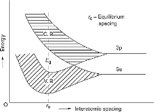
If N atoms are brought into close proximity it is quite reasonable to expect a modification in the energy states of the valence electrons. Starting with N-isolated Si atoms, and conceptually bringing the atoms closer and closer together, one finds the interatomic forces lead to a progressive spread in the allowed energies. The spread in energies gives rise to closely spaced sets of allowed-states is known as energy bands.
An isolated atom possesses discrete energies of different electrons. Suppose two isolated atoms are brought to very close, then the electrons in the orbits of two atoms interact with each other. So, that in this system, the energies of electrons will not be in the same level but changes and the energies will be slightly lower and larger than the original value. So, at the place of each energy level, a closely spaced two energy levels exists.
If ‘N’ number of atoms are brought together to form a solid and if these atoms’ electrons interact and give ‘N’ number of closely spaced energy levels in the place of discrete energy levels, it is known as bands of allowed energies. Between the bands of allowed energies, there are empty energy regions, called forbidden band of energies.
|
Figure 1: Formation of energy bands in solids
Kronig-Penney model shows the existence of band gap. Kronig-Penney model supports the existence of these bands of energies (allowed bands and forbidden bands).
The formation of energy bands has been explained taking Sodium (Na) metal as an example. When isolated sodium atoms are brought together to form a solid, then the energy levels of the valence electrons spread into bands. The 3S and 3P orbitals electrons energies are shown in Figure 1. These bands are seen to overlap strongly at the interatomic spacing of sodium.
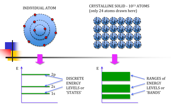
We know that atoms have discrete energy levels. When a huge number of atoms are combined to form a solid, these discrete energy levels are replaced by discrete ranges of energy or called as energy bands.
In energy bands there are so many individuals allowed energy values or you can say that the energy bands the energy distribution is continuous. This is shown in the following figure
|
Figure 2: Energy Level and energy band
In between energy bands are ranges of energy which are entirely impossible known as band gaps
Different substances have different band structures which explain the characteristics of that substance in terms of electrical conduction.
Bands are formed by the closely spaced orbitals.
There are three types of bands:
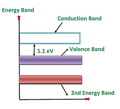
1. Valance Bands: Valence band it is a group of orbitals which contain electrons in the shell. Or we can say It is also defined as the energy band that comprises of valence electrons present in the outermost shell of an atomic structure.
These valence electrons, when provided with sufficient energy, get changed into free electrons and moves to conduction band thereby causing conductivity. It is at a lower energy level than the conduction band in the energy level diagram.
2. Conduction Band: Conduction band is a group of empty orbitals of the shells that do not contain any electron due to their configuration making the orbitals of higher energy levels.
When the electrons pass from valance band to the conduction band these solids conduct electricity with flow of charges in the form of electrons.
3. Forbidden Energy Band: These two bands are separated by a certain amount of energy known as the forbidden energy gap. In this band not a single electron is available. It diagrams it is named as Band Gap.
2.1.2 CLASSIFICATION OF SOLIDS BASED ON BAND THEORY
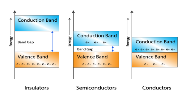
Let us distinguish between conductor, semiconductors and insulator on the basis of these bands.
|
Figure 3: Classification of Solids Based On Band Theory
In Conductors: The valance band and the conduction band overlap each other. This makes it easy for the electricity to pass through them. In conductors, the valence band is either not fully occupied with electrons, or the filled valence band overlaps with the empty conduction band. In general, both states occur at the same time, the electrons can therefore move inside the partially filled valence band or inside the two overlapping bands. In conductors there is no band gap between the valence band and conduction band.
In Semi-conductors: there is a slight gap between the conduction band and the valance band. This band gap is less than or equal to 1.4 eV. The electrons from valance shell take a little energy to excite from valance band to the conduction band. Even in semiconductors, there is a band gap, but compared to insulators it is so small that even at room temperature electrons from the valence band can be lifted into the conduction band. The electrons can move freely and act as charge carriers.
In Insulators: In insulators the valence band is fully occupied with electrons due to the covalent bonds. To achieve conductivity, electrons from the valence band have to move into the conduction band. the energy gap is considerably large and the electrons of the valance band cannot be excited to the conduction band before the melting or the dissociation of the solid. This means that under the practically ambient condition it cannot conduct electricity.
2.1.3 ENERGY BAND DIAGRAM OF GERMANIUM & SILICON
Consider an isolated silicon atom; its energy levels are quantized. When two identical atoms are brought closer together, the quantized energy levels hybridize and split into two different levels because of the mutual interaction of the two atoms. More generally, when N atoms are moved closer, until they reach the equilibrium inter-atomic distance d, the energy levels split into N levels. These N levels are very close to each other if N is large (which is the case in a crystal) so that they eventually form a continuous energy band.
Germanium was discovered in 1886. It is an earth element from the flue dust of zinc smelters. The recovered germanium is in the form of germanium dioxide powder. It is then converted into pure germanium. Its atomic number is 32. It has 32 protons in the nucleus and 32 electrons distributed in the four orbits around the nucleus. The number of electrons in the first, second, third and fourth orbit is 2, 8, 18 and 4 respectively. It is clear that the germanium has four valence electrons. The various germanium atoms are held together through covalent bonds.
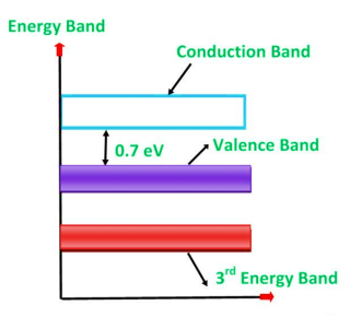
The forbidden energy gap (i.e. the gap between the valence band and conduction band) in this material is very small. Hence, very small energy is sufficient to lift the electrons from the valence band to the conduction band.
Energy band diagram for germanium is given in figure
|
Figure 4: Energy band diagram of germanium
Silicon is the element available in most of the common rocks. Actually, sand is silicon dioxide. It is treated chemically and reduced to pure silicon, which can be used for the preparation of electronic devices. ts atomic number is 14. Therefore, it has 14 protons in the nucleus and 14 electrons distributed in the three orbits around the nucleus. The number of electrons in the first, second and third orbit is 2, 8 and 4 respectively. The various silicon atoms are held together through covalent bonds.
The forbidden energy gap in this material is quite small. It also needs small energy to lift the electrons from the valence band to the conduction band.
Therefore, even at room temperature, a minute quantity of valence electrons is lifted to the conduction band and constitute current conduction if a high electric field is applied. However, at room temperature, the number of electrons lifted to the conduction band in the case of silicon is quite less than germanium.
|
Figure 5: Energy band diagram of silicon
Key Takeaways
Energy Bond Model gives the energy aspect of atoms to get good knowledge of semiconductor.
The spread in energies gives rise to closely spaced sets of allowed-states is known as energy bands.
Bands are formed by the closely spaced orbitals.
There are three types of bands: Valence band, conduction band, Forbidden Energy Band
The Valence band and conduction band are separated by a certain amount of energy known as the forbidden energy gap.
Insulators are those having wide band gap.
Metals: very small or no band gap exists at all due to an overlap of the valence and conduction bands
Semiconductors is an intermediate case
On the basis of band theory, we can classify the materials as conductors, semiconductors, and insulators based on these bands.
The Fermi function gives the probability of occupying an available energy state, but this must be factored by the number of available energy states to determine how many electrons would reach the conduction band.
When the temperature is not at absolute zero, the material will be receiving thermal energy from surroundings. However, at ordinary temperature, the amount of energy an electron can gain is quite small, because of which the electrons occupying energy levels below the Fermi level.
However, there are unoccupied higher energy levels which are above the occupied energy levels at small energy differences. They are located near Fermi level. Those are the energy levels into which, the electrons in the energy levels near Fermi level, are capable of being excited.
During thermal excitation when the temperature is greater than 0K (i.e., T >0), the electrons which absorb the thermal energy move into higher energy levels which were unoccupied at zero degree absolute (i.e., T = 0).
Such excitations seem to be random, the occupation of various energy level obey a statistical distribution called Fermi-Dirac distribution’s
Fermi function F (E):
Fermi-Dirac distribution function represents the probability of an electron occupying a given energy level at absolute temperature. It is given by Fermi factor F(E) or f(E).

Where KB Boltzmann Constant
T Temperature
If g(E) is the density of states and f(E) gives the probability of occupation of those states at a given temperature, the number of occupied states, n(E), is given by
n(E) =  (1)
(1)
If the number of occupied states in an energy band needs to be calculated the integration needs to be performed over the entire band. This will be a function of temperature, since the Fermi function is temperature dependent. Equation 1 can be used to calculate the concentration of electron and holes in semiconductors, which decides their conductivity.
Effect of temperature on Fermi Function:
Case (i) Probability of occupation for E < EF at T = 0K

When T = 0K and E < EF, we have
F(E) =  =
=  = 1
= 1
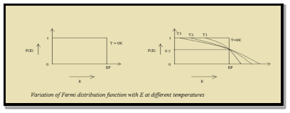
Thus at T = 0K, there is 100 % chance for the electrons to occupy the energy levels below the Fermi level.
|
Figure 6: Fermi distribution
Case (ii) Probability of occupation for E>EF at T = 0K
When T = 0K and E > EF, we have
F(E) =  =
=  =
=  = 0
= 0
Thus, there is 0 % chance for the electrons to occupy energy levels above the Fermi energy level. From the above two cases, at T = 0K the variation of F(E) for different energy values becomes a step function.
Case (iii) Probability of occupation at ordinary temperature
At ordinary temperature, the value of probability starts reducing from 1 for values of E slightly less than EF. With the increase of temperature, i.e., T> 0K, Fermi function F (E) varies with E.
At any temperature other than 0K and E = EF
F(E) =  =
=  =
=  = 50%
= 50%
Hence, there is 50 % chance for the electrons to occupy Fermi level. Further, for E > EF the probability value falls off rapidly to zero.
Case (iv) At high temperature
When kT >> EF, the electrons lose their quantum mechanical character and Fermi distribution function reduces to classical Boltzmann distribution
Key Takeaways
The Fermi function gives the probability of occupying an available energy state,
Fermi-Dirac distribution function represents the probability of an electron occupying a given energy level at absolute temperature. It is given by Fermi factor F(E) or f(E).

Thus at T = 0K, there is 100 % chance for the electrons to occupy the energy levels below the Fermi level.
At any temperature other than 0K and E = EF, there is 50 % chance for the electrons to occupy Fermi level.
At high temperature, the electrons lose their quantum mechanical character and Fermi distribution function reduces to classical Boltzmann distribution
FERMI ENERGY
Intrinsic semiconductors—carrier concentration
Here we will calculate the number of electrons excited into the conduction band at temperature T and also the hole concentration in the valence band. It is assumed that the electrons in the conduction band behave as if they are free particles with effective mass me* and the holes near the top of the valence band behave as if they are free particles with effective mass mh*.
Here we will calculate the electron concentration, hole concentration
The density of Electrons in Conduction Band
The number of free electrons per unit volume of a semiconductor having energies in between E and E + dE is represented as N(E) dE
dE = width of Energy band
Therefore, we have:
N(E) dE = ge(E) dE fe(E) ………. (1)
ge(E) = The density of electron states per unit volume
fe(E) = Fermi-Dirac distribution function i.e. probability that an electron occupies an electron state
The number of electrons present in the conduction band per unit volume of material ‘n’ is obtained by integrating N(E) dE between the limits Ec and Ect
Where Ec = the bottom energy levels of the conduction band
Ect = the bottom and top energy levels of the conduction band
n = can be written as n = n = we know that above Ect, there are no electrons. Hence, Equation (3) becomes n = n = The Fermi-Dirac distribution function fe(E) can be represented as:
Compared to the exponential value, so the ‘1’ in the denominator can be neglected. So Hence, The density of electron states ge(E) in the energy space from E = 0 to E can be written as:
where me* is the effective mass of an electron and h is Planck’s constant.
To evaluate n, the density of states is counted from Ec, since the minimum energy state in the conduction band is Ec. so eq (8) can become
Substituting Equations (6) and (9) in (4) gives n = n = The above equation can be simplified by the following substitution: Put ɛ = E − Ec ………… (11) So, dɛ = dE In Equation (11), Ec is constant, as we change the variable E to ε in Equation (10), the integral limits also change. In Equation (11), as E → Ec then ε → 0 and E → ∞, then ε also → ∞. the exponential term in Equation (10) becomes:
Substituting Equations (11) and (12) in (10), we get: n = n = Above integral (I) can be simplified by substitution. Put ε = x2 so that dɛ = 2x dx I = = = Substituting Equation (14) in (13) gives: n = n = n = n = The term n =Nc The density of Holes in Valence Band The number of holes per unit volume of semiconductor in the energy range E and E + dE in the valence band is represented as P(E) dE. Proceeding the same way (as in the case of electrons) we have Therefore, we have: P(E) dE = gh(E) dE fh(E) ………. (17) dE = width of Energy band gh(E) = The density of holes’ states per unit volume fh(E) = Fermi-Dirac distribution function i.e. probability that a hole occupies an electron state The number of electrons present in the conduction band per unit volume of material ‘n’ is obtained by integrating P(E) dE between the limits Evb and EV where EV = the bottom energy levels of the valence band Evb = the bottom and top energy levels of the valence band The total number of holes present in the valence band per unit volume of material ‘p’ is obtained by integrating P(E) dE
Equation (18) can be represented as:
Now we know that below Evb no holes are present. Hence, Equation (19) becomes
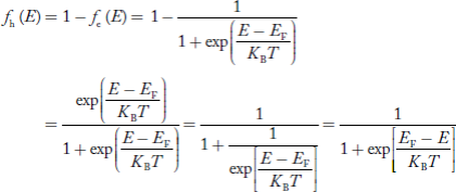
We know a hole can also be defined as the absence of an electron. presence of a hole = the absence of an electron Hence, the Fermi-Dirac function of holes fh(E) in the valence band is:
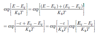
Compared to exponential, the ‘1’ in the denominator is negligible, Hence,
The density of hole states between E and E + dE in valence band can be written similar to Equation (8.9) for electrons.
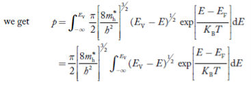
Where mh* is the effective mass of the hole. Substituting Equations (21) and (22) in (20),
The above equation can be simplified by the substitution: Put ɛ = EV − E ............. (24) so dɛ = − dE In Equation (24), EV is constant, as we change the variable E to ε in Equation (23), the integral limits also change. In Equation (24), as E → EV then ε → 0 and E→ −∞, then ε → ∞ the exponential term in Equation (23) becomes:
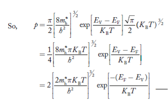
Substituting Equations (24) and (25) in (23), we get:
From Equation (14), we know the integral value
….The term
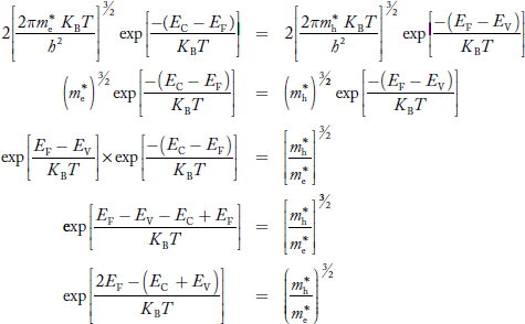
Fermi Level We know that in an intrinsic semiconductor Electron concentration ‘n’ = Hole concentration ‘p’ Equating Equations (15) and (27), we get
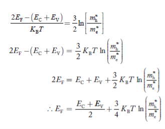
Taking logarithms on both sides, we get
Normally, mh* is greater than me*, since ln Temperature effect on Fermi level Fermi level slightly rises with an increase of temperature. But in the case of a pure intrinsic semiconductor like Si and Ge, mh* ≈ me* So in these cases, the Fermi level lies in the middle of the energy gap. DEPENDENCE OF FERMI ENERGY ON CARRIER CONCENTRATION AND TEMPERATURE (QUALITATIVE)- Carrier Concentration in Extrinsic Semiconductors The number of charge carriers presents per unit volume of a semiconductor material is called carrier concentration. Suppose donor and acceptor atoms are doped in a semiconductor. At temperature T K, n = number of conduction electrons p = number of holes N−A = number of acceptor ions N+D = number of donor ions We know that the below equation holds good in the semiconductor. The total negative charge due to conduction electrons and acceptor ions is equal to holes and donor ions in a unit volume of material. So the material will be considered neutral if, n + N−A = p + N+D ………. (34) Equation (34) is called the charge neutrality equation. In the above equation
concentration of acceptor ions N−A = acceptor concentration x probability of finding an electron in acceptor level
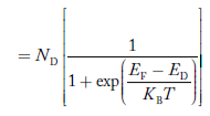
Similarly, the donor ions concentration is
In n-type material Note nn represents electrons in n-type material pn represents holes’ concentration in n-type material. there are no acceptor atoms so N−A = 0.
|
At 0 K, all the electron states at the donor level are occupied by electrons.
As the temperature is increased from 0 K, some of the electrons jump from these donor states into the conduction band.
Also, the concentration of holes is extremely less compared with the concentration of conduction electrons [p << n]
From Equation (34) we have
n = p N+D
(Or) n ≈ N+D ………… (38) [since p << N+D]
At temperature T K,
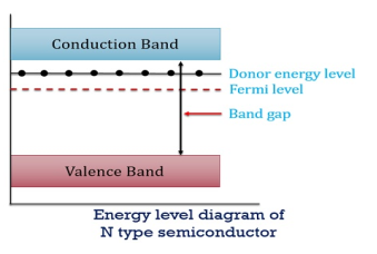
As the temperature increase, almost all the donor atoms donate electrons to the conduction band.
|
Figure 7: Energy level diagram of N type semiconductor
So, in n-type material, the free electron concentration is almost equal to the donor atoms.
So we can rewrite the above equation as
nn ≈ ND ……………. (39)
where nn represents electrons in n-type material
also, the hole concentration in n-type material can be obtained by applying the law of mass action nn pn =ni2
 …………. (40)
where pn represents holes’ concentration in n-type material.
In n-type material at 0 K, the Fermi energy level lies in the middle of Ec and ED

At temperature> 0K
 ………. (41)
With the increase in temperature, the Fermi level shifts upwards according to Equation (61) slightly due to the ionization of donor atoms.
With further increase of temperature, electron-hole pairs are generated due to the breaking of covalent bonds, hence Fermi level shifts downwards.
In p-type semiconductor
Note
pp represents holes in the p-type material
np represents electrons in the p-type material
There are no donor atoms so means no ions present  = 0.
= 0.
At 0 K, all the acceptor levels are not occupied by electrons.
As the temperature is increased from 0 K, some electrons jump from top valence band energy levels to the acceptor states, leaving holes in the valence band and acceptor ions  are formed.
At some room temperature T K, the concentration of conduction electrons is extremely less compared with hole concentration.
∴ From Equation (34), we have
n + N−A = p …………… (42)
(or) N−A ≈ p ……………. (43) [since n << N−A]
At temperature T K, in p-type material,
the hole concentration is almost equal to the acceptor atoms in a unit volume of the material.
So, Equation (43) can be written as
pp ≈ NA ………………. (44)
where pp represents holes in the p-type material
The electron concentration in p-type material can be obtained by applying the law of mass action as nppp = ni2
 ……………. (45)
where np represents free electron concentration in the p-type material.
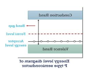
|
Figure 8: Energy level diagram of N type semiconductor.
In p-type material, the Fermi level lies in between EV and EA at 0 K
|
As the temperature is increased from 0 K, the Fermi level shifts downwards slightly as per Equation (46) due to ionization of acceptor atoms.
And with a further increase of temperature, electron-hole pairs are generated due to the breaking of covalent bonds, so the Fermi level shifts upwards.
Key Takeaways
The density of Electrons in Conduction Band
n =Nc
The density of Holes in Valence Band

Fermi level slightly rises with an increase of temperature. But in the case of a pure intrinsic semiconductor like Si and Ge, mh* ≈ me*, So in these cases, the Fermi level lies in the middle of the energy gap.
Carrier Concentration in Extrinsic Semiconductors
The donor ions concentration is

Concentration of acceptor ions N−A

Fermi Level shifts in case of extrinsic semiconductor.
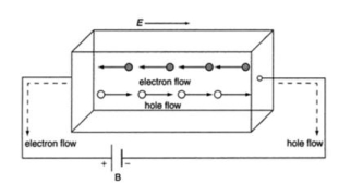
In semiconductor, the conduction band electron and valance band hole participate in electrical conduction. To obtain expression for electrical conductivity consider an intrinsic semiconductor bar which is connected to external battery as shown in figure
The electric field exist along x direction. The field accelerate electrons (conduction electrons) along negative X-direction and holes along positive X-direction. They start moving with a constant velocity called Drift velocity vd
The total current in the semiconductor (due to both electron and hole)
I = Ie +Ih
or total current density
J = Je +Jh ..........(1)
|
Figure 9: Conductivity of semiconductors
In order to find the current density of electrons, let the concentration of electrons are 'n’, charge is 'e' and drift velocity is 've', Then
Je =neve ..........(2)
The drift velocity produced per unit electric field is called 'mobility’, Thus
μe = 
or
μeE = 
substituting in equation 2
Je =neμeE ..........(3)
From Ohms law,
J = E where Je = eE
Je =neμeE = eE ..........(4)
e = neμe ..........(5)
Similarly, current density for holes
Jp =peμpE = pE ..........(6)
And conductivity
p = peμp ..........(7)
Substituting value of Je and Jp from eq 4 and 6 in eq 1, we get
J = neμeE + peμpE
J = (neμe + peμp) E ..........(8)
From Ohms law J = E
= neμe + peμp
where e = neμe and p = peμp
Also ni =CT3/2e -Eg/2kT ..........(9)
Therefore
= nie (μe + μp) = CT3/2e -Eg/2kT e (μe + μp) ..........(10)
The mobilities of carrier depend upon temperature as
μ 

For Electrons μe
 and for holes μp

μe + μp= =
=  ..........(11)
Using equation 11 in equation 10
= CT3/2e -Eg/2kT e
= C e e -Eg/2kT
Let B = C e we get
= Be -Eg/2kT ..........(12)
Key Takeaways
In semiconductor, the conduction band electron and valance band hole participate in electrical conduction.
The electric field exist along x direction. The field accelerate electrons (conduction electrons) along negative X-direction and holes along positive X-direction. They start moving with a constant velocity called Drift velocity vd
The total current in the semiconductor is due to both electron and hole i.e.
I = Ie +Ih
Current density is given as J = (neμe + peμp) E
The mobilities of carrier depend upon temperature as μ 

A P-N Junction Diode is formed by doping one side of a piece of silicon with a P-type dopant (Boron) and the other side with a N-type dopant (phosphorus). Ge can be used instead of Silicon. The P-N junction diode is a two-terminal device. This is the basic construction of the P-N junction diode. It is one of the simplest semiconductor devices as it allows current to flow in only one direction.
ZERO BIASED CONDITION
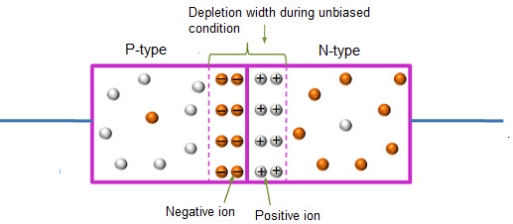
In this case, no external voltage is applied to the P-N junction diode; and therefore, the electrons diffuse to the P-side and simultaneously holes diffuse towards the N-side through the junction, and then combine with each other. Due to this an electric field is generated by these charge carriers. The electric field opposes further diffusion of charged carriers so that there is no movement in the middle region. This region is known as depletion width or space charge.
|
Figure 10: Unbiased or zero biased PN Junction Diode
FORWARD BIAS
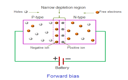
In the forward bias condition, the positive terminal of the battery is connected to the P-Type material and the negative terminal of the battery is connected to the N-type material. This connection is also called as giving positive voltage.
|
Figure 11: Forward bias
Electrons from the N-region cross the junction and enters the P-region. Due to the attractive force that is generated in the P-region the electrons are attracted and move towards the positive terminal. Simultaneously the holes are attracted to the negative terminal of the battery. By the movement of electrons and holes current flows. In this condition, the width of the depletion region decreases due to the reduction in the number of positive and negative ions.
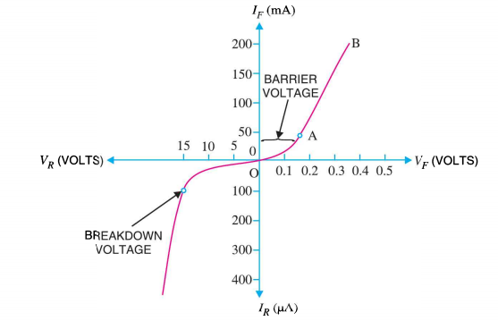
If this external voltage Vf becomes greater than the value of the potential barrier, approx. 0.7 volts for silicon and 0.3 volts for germanium, the potential barriers opposition will be overcome and current will start to flow.
This is because the negative voltage pushes or repels electrons towards the junction giving them the energy to cross over and combine with the holes being pushed in the opposite direction towards the junction by the positive voltage. This results in a characteristics curve of zero current flowing up to this voltage point, called the “knee” on the static curves and then a high current flow through the diode with little increase in the external voltage as shown in I-V characteristics.
REVERSE BIAS
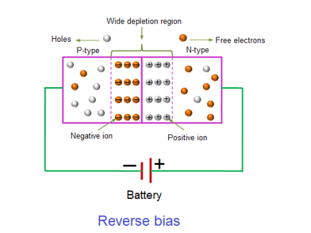
In the reverse bias condition, the negative terminal of the battery is connected to the P-type material and the positive terminal of the battery is connected to the N-type material. This connection is also known as giving negative voltage.
|
Figure 12: Reverse bias
The positive voltage applied to the N-type material attracts electrons towards the positive electrode and away from the junction, while the holes in the P-type end are also attracted away from the junction towards the negative electrode.
The net result is that the depletion layer grows wider due to a lack of electrons and holes and presents a high impedance path, almost an insulator. The result is that a high potential barrier is created thus preventing current from flowing through the semiconductor material.
This condition represents a high resistance value to the PN junction and practically zero current flows through the junction diode with an increase in bias voltage. However, a very small leakage current does flow through the junction which can be measured in micro-amperes, (μA).
If the reverse bias voltage Vr applied to the diode is increased to a sufficiently high enough value, it will cause the diode’s PN junction to overheat and fail due to the avalanche effect around the junction. This may cause the diode to become shorted and will result in the flow of maximum circuit current, and this shown as a step downward slope in the reverse static characteristics curve in I-V characteristics.
I-V CHARACTERISTICS OF PN JUNCTION DIODE
The I-V Characteristic Curves, which is short for Current-Voltage Characteristic Curves or simply I-V curves of an electrical device
The application of a forward biasing voltage on the junction diode results in the depletion layer becoming very thin and narrow which represents a low impedance path through the junction thereby allowing high currents to flow. The point at which this sudden increase in current takes place is represented on the static I-V characteristics curve above as the “knee” point. The current starts increasing with increase in voltage. At knee voltage current shows a sharp increment in its magnitude. This behaviour is mentioned above. As large current flow in forward biasing so we measure this current in mA.
When a junction diode is Reverse Biased, the thickness of the depletion region increases and the diode acts like an open circuit blocking current flow. So only a very small leakage current will flow.
|
Figure 13: I-V characteristics
Note in addition that the minority carrier drift currents are not affected by the height of the potential bill. It is the number of minority carriers wandering into the depletion region per second that determines the current flow.
The situation is similar to a waterfall. The water flowing over the falls is independent of the height of the falls. the overall 1-V dependence is concluded to be of the general form 1-V characteristics.
|
Equation (1) is identical to the ideal diode equation if VA is set equal to kT/q.
Key Takeaways
A P-N Junction Diode is formed by doping one side of a piece of silicon with a P-type dopant (Boron) and the other side with a N-type dopant (phosphorus). Ge can be used instead of Silicon.
Zero biased condition is the case when no external voltage is applied to the P-N junction diode.
In the forward bias condition, the positive terminal of the battery is connected to the P-Type material and the negative terminal of the battery is connected to the N-type material. This connection is also called as giving positive voltage.
In the reverse bias condition, the negative terminal of the battery is connected to the P-type material and the positive terminal of the battery is connected to the N-type material. This connection is also known as giving negative voltage.
The Voltage drop across the depletion region under equilibrium conditions, known as the built-in potential (Vbi), is a junction’s parameter of sufficient importance to merit further consideration.
We will now find a relationship for Vbi. Consider a non-degenerately doped pn junction maintained under equilibrium conditions with x = 0 positioned at the metallurgical boundary. The ends of the equilibrium depletion region are taken to occur at — xp and xp on the p- and n-sides of the junction respectively
We know
Integrating across the depletion region gives
…………… (2) Under equilibrium conditions.
Solving for ξ in equation (3) and making use of the Einstein relationship. We obtain Substituting Equation (4) into Equation (2), and completing the integration then yields For the specific case of a non-degenerately doped step junction where ND and NA are the n- and p-side doping concentrations, one identities. and therefore
|
It is useful to perform a sample computation to gauge the relative magnitude of the built in voltage. Choosing ND= NA = 1015/ cm3 and a Si diode maintained at 300 K,
One computes Vbi= (0.0259) ln(1030/1020)  0.6 V. This is a typical result. In non-degenerately doped diodes Vbi < EG/q, or Vbi is less than the band gap energy converted into volts. Non-degenerately doped Ge, Si, and GaAs diodes maintained at room temperature exhibits a Vbi less than 0.66 V, 1.12 V. and 1.42 V respectively.
From the energy band diagram, we observed
Clearly, for a Non-degenerately doped diode bosh (Ei — EF) p-side, and (EF — Ei) n-side are less than EG/2, making Vbi < EG/q Moreover, in a Non-degenerately doped step junction under equilibrium conditions,
|
Equations (12 and13) and Equation (9) are valid only for Non-degenerately dopings, there are no doping-related restrictions on the validity of Equation (11).
Key Takeaways
The Voltage drop across the depletion region under equilibrium conditions, known as the built-in potential (Vbi), is a junction’s parameter of sufficient importance to merit further consideration.
It is given by
When the magnetic field is applied perpendicular to a current-carrying conductor, then a voltage is developed in the material perpendicular to both the magnetic field and current in the conductor. This effect is known as Hall Effect and the voltage developed is known as Hall voltage (VH).
Hall Effect is useful to identify the nature of charge carriers in material and hence to decide whether the material is an n-type semiconductor or p-type semiconductor, also to calculate carrier concentration and mobility of carriers.
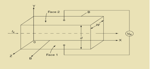
Hall Effect can be explained by considering a rectangular block of an extrinsic semiconductor in which current is flowing along the positive X-direction and magnetic field B is applied along Z-direction as shown in Figure.
|
Figure 14: Hall Effect
Suppose if the semiconductor is n-type, then mostly the carriers are electrons and the electric current is due to the drifting of electrons along negative X-direction or if the semiconductor is p-type, then mostly the carriers are holes and the electric current is due to drifting of the holes along positive X-direction.
As these carriers are moving in the magnetic field in the semiconductor that means they experience Lorentz force represented by FL
FL = Bevd
Where vd is the drift velocity of the carriers. (already explained in the previous section).
We can obtain the direction of this force by applying Fleming’s left-hand rule in electromagnetism.
Fleming’s left-hand rule can be explained as If we stretch the thumb, forefinger, and middle finger in three perpendicular directions so that the forefinger is parallel to the magnetic field and the middle finger is parallel to the current direction, then the thumb represents the direction of the force on the current-carrying carriers.
So the Lorentz force is exerted on the carriers in the negative Y-direction. Due to Lorentz force, more and more carriers will be deposited at the bottom face (represented by face 1in the figure) of the conductor.
The deposition of carriers at the bottom face is continued till the repulsive force due to accumulated charge balances the Lorentz force.
After some time of the applied voltage, both the forces become equal in magnitude and act in opposite direction, then the potential difference between the top and bottom faces is equal to Hall voltage and that can be measured.
At equilibrium, the Lorentz force on a carrier
FL = Bevd ……………. (1)
and the Hall force
FH = eEH ……………. (2)
Where EH is the Hall electric field due to accumulated charge.
At equilibrium, FH = FL
eEH = Bevd
∴ EH = Bvd ……………. (3)
If ‘d’ is the distance between the upper and lower surfaces of the slab, then the Hall field
EH =  ……………..(4)
In n-type material, Jx = –nevd
vd = -  ……………..(5)
Where n is free electron concentration, substituting (5) in (3), we have
∴ EH = -B  ……………..(6)
For a given semiconductor, the Hall field EH is proportional to the current density Jx and the intensity of magnetic field ‘B’ in the material.
i.e. EH ∝ JxB
(or) EH = RHJxB ……………. (7)
Where RH = Hall coefficient
Equations (6) and (7) are the same so, we have
RHJxB =-B 
RH = -  = -
= -  ……………..(8)
Where ρ is the charge density
Similarly, for p-type material
RH =  =
= ……………..(9)
Using Equations (8) and (9), carrier concentration can be determined.
Thus, the Hall coefficient is negative for n-type material. In n-type material, as the more negative charge is deposited at the bottom surface, so the top face acquires positive polarity and the Hall field is along negative Y-direction. The polarity at the top and bottom faces can be measured by applying probes.
Similarly, in the case of p-type material, a more positive charge is deposited at the bottom surface. So, the top face acquires negative polarity and the Hall field is along positive Y-direction. Thus, the sign of the Hall coefficient decides the nature of (n-type or p-type) material.
The Hall coefficient can be determined experimentally in the following way:
Multiplying Equation (7) with ‘d’, we have
EHd = VH = RHJxBd ……………. (10)
From (Figure 14) we know the current density Jx
Jx = 
Where W is the width of the box. Then, Equation (10) becomes
VH = RH Bd = RH
RH =  ……………..(11)
Substituting the measured values of VH, Ix, B, and W in Equation (11), RH is obtained. The polarity of VH will be the opposite for n- and p-type semiconductors.
The mobility of charge carriers can be found by using the Hall effect, for example, the conductivity of electrons is
n = neμn
Or we can rewrite it as
μn =  =n RH ……………..(12)
by using equation (11)
μn = n ……………..(13)
Applications of Hall Effect
• Using magnetic flux leakage – To properly inspect items such as pipes or tubes, Hall Effect probes work with something called magnetic flux leakage. This is a way of testing such items, and being able to spot potential corrosion, erosion, or pitting. This is specifically used in steel items and can give important information about lifespan or safety.
• Sensors to detect rotation speed – A Hall Effect probe can be used in bicycle wheels, speedometers in the automotive world, electronic types of ignition systems, and gear teeth.
• Used to detected movement – You will often find a Hall Effect probe used in such items as Go-Kart controls, smartphones, paintball guns, or airsoft guns, as well as some GPS systems.
• Ferrite Toroid Hall Effect current transducers – This is mainly used in electronic compasses, making use of the magnetic field to show direction.
• Split-ring clamp-on sensors – These types of Hall Effect probes are used to test equipment without having to take the whole circuit board apart, e.g. complex items.
• Analog multiplication – Anything which needs a power measurement, e.g. sensing, and is also used in small computers.
• General power measurement – Any device which needs to be tested for its power input can be done by a Hall Effect probe.
• Position and motion sensors – This is mainly used in a DC motor, often the brushless type.
• The automotive world – Hall Effect probes are used widely in the automotive world, especially in fuel injection and ignition. Wheel rotation sensors also use Hall Effect probes, e.g. for anti-lock braking.
For determination of the type of given semiconductor.
For N-type, Hall coefficient RH= negative
For P-type, Hall coefficient RH= Positive
To determine carrier concentration n and p; that is n=p=1/e𝑅𝐻
Determination of mobility of charge carriers μn =  =n RH. Where 𝜎= electrical conductivity
To determine the sign of charge carriers whether the conductivity is due to electrons or holes.
Main Advantages of Using Hall Sensors
Why is a Hall Effect probe advantageous in all of these instances? Because the probes are not affected by outside influences, e.g. water or dirt. They can also easily sense the measure of the output they need when they are placed in the right position. On top of this, Hall Effect probes are safer, because the voltage never actually makes it directly to the sensor/probe. This makes this type of measurement overall so much safer than other methods.
As you can see, understanding how something is put into practice in the real world helps you to understand it in real terms. The Hall Effect is certainly very commonplace these days, in much more methods and applications than we realize. While certainly very useful in the automation world, even basic items such as a compass make large use of this scientific approach.
Key Takeaways
When the magnetic field is applied perpendicular to a current-carrying conductor, then a voltage is developed in the material perpendicular to both the magnetic field and current in the conductor. This effect is known as Hall Effect.
The voltage developed is known as Hall voltage (VH).
Hall Effect is useful to identify the nature of charge carriers in material and hence to decide whether the material is an n-type semiconductor or p-type semiconductor.
Hall Effect also to calculate carrier concentration and mobility of carriers.
Hall coefficient is given by RH = -  = -
= -  Where ρ is the charge density
Hall coefficient is given by RH = 
Mobility of charge carriers can be found by using the Hall Effect μn = n
Bipolar junction transistor or BJT is simply known as Transistor. A transistor consists of two pn junctions formed by sandwiching either p-type or n-type semiconductor between a pair of opposite types.
The prefix 'trans' means the signal transfer property of the device while 'istor ' classifies it as a solid element in the same general family with resistors.
Accordingly, there are two types of transistors
n-p-n transistor
p-n-p transistor
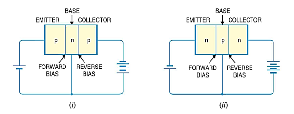
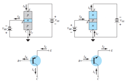
An n-p-n transistor is composed of two n-type semiconductors separated by a thin section of p-type as shown in Figure 15 (i).
However, a p-n-p transistor is formed by two p-sections separated by a thin section of n-type as shown in Figure 15(ii).
|
Figure 15: (i) n-p-n transistor (ii) p-n-p transistor
In each type of transistor, the following points may be noted:
Transistor may be regarded as a combination of two diodes connected back to back.
There are three terminals, one taken from each type of semiconductor.
The middle section is a very thin layer. The thin layer plays an important role in the function of a transistor.
A transistor has two pn junctions. one junction is forward biased and the other is reverse biased. The forward biased junction has a low resistance path whereas a reverse biased junction has a high resistance path. The weak signal is introduced in the low resistance circuit and output is taken from the high resistance circuit. Therefore, a transistor transfers a signal from a low resistance to high resistance.
A transistor (pnp or npn) has three sections of doped semiconductors. The section on one side is the emitter and the section on the opposite side is the collector. The middle section is called the base and forms two junctions between the emitter and collector.
|
Figure 16: (i) p-n-p transistor (ii) n-p-n transistor
Emitter: The section on one side that supplies charge carriers (electrons or holes) is called the emitter. The emitter is always forward biased w.r.t. base so that it can supply a large number of majority carriers. In Figure 16 (i), the emitter (p-type) of pnp transistor is forward biased and supplies hole charges to its junction with the base. Similarly, in Figure 16 (ii), the emitter (n-type) of npn transistor has a forward bias and supplies free electrons to its junction with the base.
Collector: The section on the other side that collects the charges is called the collector. The collector is always reverse biased. Its function is to remove charges from its junction with the base. In Figure 16 (i), the collector (p-type) of pnp transistor has a reverse bias and receives hole charges that flow in the output circuit. Similarly, In Figure 16 (ii), the collector (n-type) of npn transistor has reverse bias and receives electrons.
Base: The middle section which forms two pn junctions between the emitter and collector is called the base. The base emitter junction is forward biased allowing low resistance for the emitter circuit. The base-collector junction is reverse biased and provides high resistance in the collector circuit.
Before studying action of transistor, some important facts about transistor should be keep in mind.
The transistor has two pn junctions i.e. it is like two diodes. The junction between emitter and base may be called emitter-base diode or simply the emitter diode. The junction between the base and collector may be called collector-base diode or simply collector diode.
The emitter diode is always forward biased whereas collector diode is always reverse biased.
Three regions of transistor are emitter, base and collector. The base is much thin as compared to emitter while "collector is wider than both. To keep it simple it is assumed emitter and collector is considered to be of same size.
The emitter is heavily doped so that it can inject a large number of charge carriers (electrons or holes) into the base. The base is lightly doped and very thin it passes most of the emitter injected charge carriers to the collector. The collector is moderately doped.
The resistance of emitter diode (forward biased) is very small as compared to collector diode (reverse biased). Therefore, forward bias applied to the emitter diode is generally very small whereas reverse bias on the collector diode is much higher.
Working of Transistor
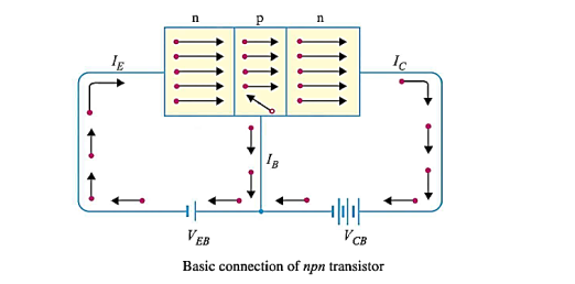
Working of npn transistor: As discussed in the npn transistor emitter-base junction is forward biased to emitter-base junction and collector-base junction is reverse biased. The forward bias causes the electrons in the n-type emitter to flow towards the base. This constitutes the emitter current Ie.
Ie = Ib + Ic
|
Figure17: n-p-n transistor
As these electrons flow through the p-type base, they tend to combine with holes. As the base is lightly doped and very thin, therefore, only a few electrons (less than 5%) combine with holes to constitute base current Ib. The remainder i.e. more than 95% cross over into the collector region to constitute collector current Ic in this way, almost the entire emitter current flows in the collector circuit. It is clear that emitter current is the sum of collector and base currents i.e.
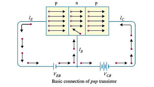
Working of pnp transistor: In the pnp transistor emitter-base junction is forward biased to emitter-base junction and collector-base junction is reverse biased. The forward bias causes the holes in the p-type emitter to flow towards the base. This constitutes the emitter current Ie. As these holes cross into n-type base, they tend to combine with the electrons. As the base is lightly doped and very thin, therefore, only a few holes (less than 5%) combine with the electrons.
|
Figure 18: p-n-p transistor
The remainder (more than 95%) cross into the collector region to constitute collector current Ic. In this way, almost the entire emitter current flows in the collector circuit. It may be noted that current conduction within pnp transistor is by holes. However, in the external connecting wires the current is still by electrons.
Thus the input circuit (i.e. emitter-base junction) has low resistance because of forward bias whereas output circuit (i.e. collector base junction) has high resistance due to reverse bias. As we have seen, the input emitter current almost entirely flows in the collector circuit. Therefore, a transistor transfers the input signal current from a low resistance circuit to a high-resistance circuit.
Transistor’s Configuration: -
Common Base configuration (C.B)
Common emitter Configuration (C.E)
Common Collector Configuration (C.C)
COMMON BASE CONFIGURATION
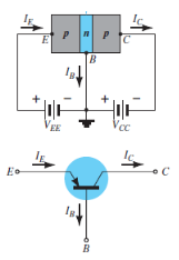
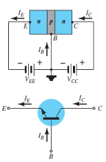
The notation and symbols of pnp and npn transistors are given below:
|
Figure 19: PNP CB and NPN CB
Here the base is common to both the input and output sides of the configuration.
The flow of holes will govern the direction of current.
Hence, Ic = Ib + Ie
Where Ic, Ib, Ie are the collector, base and emitter currents respectively.
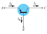
The graphical symbol of the PNP common base configuration is
|
Figure 20: PNP common base
The arrow in the above symbol shows the direction of emitter current in the device.
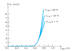
Now, to study the behaviour of the device we require two characteristics:
Input Characteristic Curve
|
Figure 21: Input Characteristic Curve
It is the relation between the input current IE to the input voltage VBE for various levels of output voltage VCB.
It is also known as driving point characteristics.
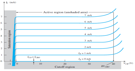
Output Characteristic Curve
|
Figure 22: Output Characteristic Curve
It is the relation between the output current IC to the output voltage VCB for various levels of input current IE.
It is also known as collector set of characteristics.
It has three basic regions:
Active Region
Here, base-emitter junction is forward biased and collector-base junction is reverse biased.
As input current IE increases above zero, output current IC increases to a magnitude equal to IE as determined by the basic transistor current relationship.
So the first approximation determined by the curve is
IC ≈ IE
Cut-off Region
It is defined as the region where the collector current IC is equal to 0A.
Here, the base-emitter junction and the collector-base junction both are in reverse bias.
Saturation Region
It is the region that lies towards the left of VCB = 0V.
Here, the base-emitter junction and the collector-base junction both are in forward bias.
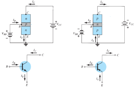
COMMON EMITTER CONFIGURATION
The notation and symbols of npn and pnp transistors are given below:
|
Figure 23: NPN CE and PNP CE
In the above figure all the currents are shown in their actual conventional directions.
The current relation developed earlier is still applicable,
IE = IB + IC
Where IE , IB , IC are the collector, base and emitter currents respectively.
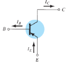
The graphical symbol of the PNP common emitter configuration is
|
Figure 24: PNP common emitter
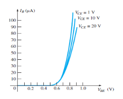
Now, to study the behaviour of the device we require two characteristics:
Input Characteristic Curve
|
Figure 25: Input Characteristic Curve
It is the graph between the input current IB to the input voltage VBE for a range of values of output voltage VCE.
Note that the magnitude IB of is in micro amperes and that of IC is in milli amperes.
Output Characteristic Curve
|
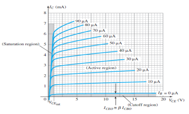
Figure 26: Output Characteristic Curve
It is the graph between the output current IC to the output voltage VCE for a range of values of input current IB.
It has three basic regions:
Active Region
Here, the base-emitter junction is forward biased and collector base junction is reverse biased.
These are the same conditions that existed in the active region of the common base configuration.
This can be employed for voltage, current or power amplification.
Cut-off Region
Here IC is not equal to zero when IB is zero.
For linear amplification purposes, it is defined as IC = ICEO.
The region below IB = 0µA is to be avoided for undistorted output signal.
When the transistor is used as a switch, the condition should be ideally IC = 0mA for a chosen VCE voltage.
Saturation Region
It is the region that lies towards the left of VCE = 0V.
COMMON COLLECTOR CONFIGURATION
The notation and symbols of npn and pnp transistors are given below:
|
Figure 27: NPN CC and PNP CC
In the above figure all the currents are shown in their actual conventional directions.
It is used for impedence matching purposes as it has high input impedence and low output impedence.
It can be designed using common emitter characteristics.
The output characteristics of common collector is same as that of common emitter configuration for all practical purposes.
The output characteristics are a plot between IE versus VCE for all values of IB.
The input current of common collector is same as that of common emitter configuration.
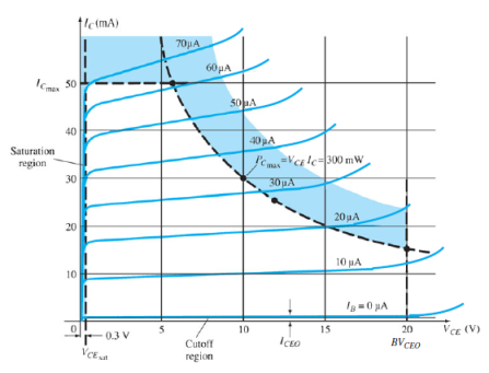
Here the region of operation will ensure that maximum ratings are not being exceeded and output ratings have minimum distortion.
|
Figure 28: Output Characteristic Curve
The characteristics specifying the minimum VCE that can be applied without entering the non-linear region is saturation region.
The maximum power dissipation is given by,
P = VCE. IC
Comparison of configuration:
Sr.no | Parameter | CB | CE | CC |
1 | Common terminal betnI/p & o/p | Base | Emitter | collector |
2 | Input Current | IE | IB | IB |
3 | Output Current | IC | IC | IE |
4 | Current Gain |
|
| ɤ= |
5 | Input Vtg. | VEB | VBE | VBC |
6 | Output Vtg. | VCB | VCE | VCC |
Key Takeaways
A transistor consists of two pn junctions formed by sandwiching either p-type or n-type semiconductor between a pair of opposite types.
There are two types of transistors n-p-n transistor and p-n-p transistor.
The emitter diode is always forward biased whereas collector diode is always reverse biased.
Three regions of transistor are emitter, base and collector. The base is much thin as compared to emitter while "collector is wider than both. To keep it simple it is assumed emitter and collector is considered to be of same size.
The emitter is heavily doped so that it can inject a large number of charge carriers (electrons or holes) into the base. The base is lightly doped and very thin it passes most of the emitter injected charge carriers to the collector. The collector is moderately doped.
Transistor’s Configuration: -Common Base configuration (C.B), Common emitter Configuration (C.E), Common Collector Configuration (C.C)
Reference Books
- Principle of electronics S. Chand V K Mehta and Rohit Mehta
- Semiconductor Device Fundamentals by Robert F. Pierret
- Introduction to Solid State Physics -- Charles Kittel
- Engineering physics- Gaur and Gupta, & S. Chand Publication
- Engineering physics - Avadhanalu and Kshirsagar, S. Chand Publication
