N type Semiconductor: -
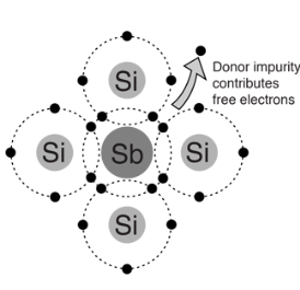
To increase the number of conduction band electrons inintrisic silicon, pentavalent imparity atoms are added. These are atoms with five valence electrons such as
i) Arsenic (as)
ii) Phosphors (p)
iii) Bismuth (Bi)
iii) Antimony ( sb)
|
- Pentavalent impurity atom in a silicon crystal. an antimony (sb) impurity atom shown above-
- Each pentavalent atom forms covalent bonds with four adjustment silicon atoms, leaving one extra electron.
- The pentavalent atom gives up on electron; it often called a donor atom.
- Majority and minority carriers: - A type here means negative charge of an electron. electron is called the majority carriers in n-type material.
- Hole in an n-type material are called minority carriers
P Type Semiconductor: -
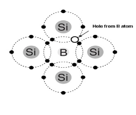
To increase the number of holes in intrinsic silicon trivalent impurity atoms are added these are atoms with their valence electrons such as
i) Baron (B)
ii) Indium (IN)
Iii) Gallium (GO)
|
- Trivalent impurity atom in a silicon crystal structure. A) Boron (B) impurity atom is shown in the center.
- The number of holes can be carefully controlled by the number of trivalent impurity atoms added to the silicon.
- A Whole created by the doping process is not accompanied by a conduction (free) electron.
- Trivalent Atom can take an electron it is often referred to as on accepted atom
Half Wave rectifier
1) Due to the unidirectional current flow through the transformer there is a possibility of core saturation to avoid this transformer size must be increased.
2) Ripple factor is high.
3) Low rectification effecting.
4) Law TUF.
5) Law D.C O/P VTG & current.
6) Large filter component are required.
ADVANTAGES: -
1) Simple Construction.
2) Component required less.
3) Small size.
APPLICATION: -
Walkman, law cost power supply.
TRANSFORMER UTILISATION FACTOR (TUF):-It indicates how well the ilp transformer is being utilized
TUF= DC O/P Power / AC power rating of the transformer

Full Wave Rectifier
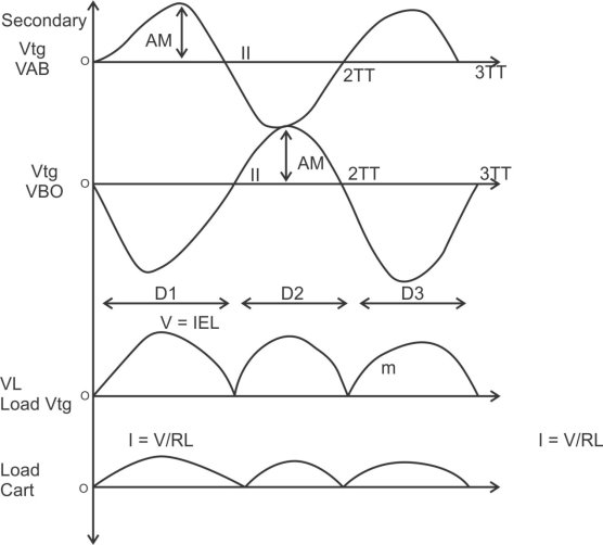
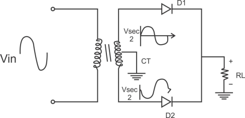
1) A center tapped rectifier is a type of full wave rectifier that uses two diode connected to the secondary of a center tapped transformer.
|
Centre tapped full wave rectifier operation: -
I) During positive half cycle of i/p ac supply.
Diagram
|
D1.Is in forward biased & D2 is in reverse biased.
II) During -ve half cycle.
|
D1 Reverse biased
D2 Forward biased
|
ADVANTAGES
1) Law ripple factor as Compared to HKR.
2) Better rectification efficiency.
3) Better TUF.
4) Higher value of average load vtg & avg load CRT.
5) No possibility of transformer core saturation.
DISADVANTAGES
PIV of diode is 2 vm,more size costly.
APPLICATION
I) Battery charges.
2) Power supply at laboratory, high current, electronic ckt.
Half Wave rectifier
1) Due to the unidirectional current flow through the transformer there is a possibility of core saturation to avoid this transformer size must be increased.
2) Ripple factor is high.
3) Low rectification effecting.
4) Law TUF.
5) Law D.C O/P VTG & current.
6) Large filter component are required.
ADVANTAGES: -
1) Simple Construction.
2) Component required less.
3) Small size.
APPLICATION: -
Walkman, law cost power supply.
TRANSFORMER UTILISATION FACTOR (TUF):-It indicates how well the ilp transformer is being utilized
TUF= DC O/P Power / AC power rating of the transformer

Full Wave Rectifier
2) A center tapped rectifier is a type of full wave rectifier that uses two diode connected to the secondary of a center tapped transformer.
|
Center tapped full wave rectifier operation:-
II) During positive half cycle of i/p ac supply.
Diagram
|
D1.Is in forward biased & D2 is in reverse biased.
II) During -ve half cycle.
|
D1 Reverse biased
D2 Forward biased
|
ADVANTAGES
1) Law ripple factor as Compared to HKR.
2) Better rectification efficiency.
3) Better TUF.
4) Higher value of average load vtg & avg load CRT.
5) No possibility of transformer core saturation.
DISADVANTAGES
PIV of diode is 2vm , more size costly.
APPLICATION
I) Battery charges.
2) Power supply at laboratory, high current, electronic ckt.
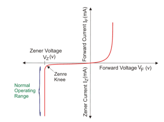
- Zener diode is a special type of p-n junction semiconductor diode in this diode the reverse breakdown voltage is adjusted precisely between 3v to 200v.
- Its applications are based on this principle hence Zener diode is called as a breakdown diode.
- The doping level of the imparity added to manufacture the zener diode is controlled in order to adjust the precise value of breakdown voltage.
PRINCIPLE OF OPERATION: - A zener diode can be forward biased or reverses biased. Its operation in the forward biased mode is same as that of a p-n junction diode but its operation in the reverse biased mode is sustainably deferent.
|
|
Numerical:
A 5.0V stabilized power supply is required to be produced from a 12V DC power supply input source. The maximum power rating PZ of the zener diode is 2W. Using the zener regulator circuit above calculate:
A). The maximum current flowing through the zener diode.
Maximum current = Watts/ Voltage =2W/5V =400mA
B). The minimum value of the series resistor, RS
 = 17.5 Ω
c). The load current IL if a load resistor of 1kΩ is connected across the zener diode.

d). The zener current IZ at full load.
Iz =Is -Il =440mA – 5mA = 395mA
The three types of configurations are Common Base, Common Emitter and Common Collector configurations. In every configuration, the emitter junction is forward biased and the collector junction is reverse biased.
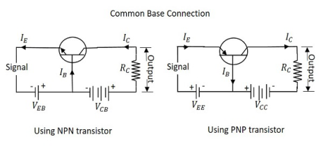
The three types of configurations are Common Base, Common Emitter and Common Collector configurations. In every configuration, the emitter junction is forward biased and the collector junction is reverse biased. Common Base CB
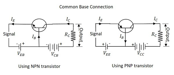
The name itself implies that the Base terminal is taken as common terminal for both input and output of the transistor. The common base connection for both NPN and PNP transistors is as shown in the following figure.
For the sake of understanding, let us consider NPN transistor in CB configuration. When the emitter voltage is applied, as it is forward biased, the electrons from the negative terminal repel the emitter electrons and current flows through the emitter and base to the collector to contribute collector current. The collector voltage VCB is kept constant throughout this.
In the CB configuration, the input current is the emitter current IE and the output current is the collector current IC.
Current Amplification Factor α
The ratio of change in collector current ΔIC to the change in emitter current ΔIE when collector voltage VCB is kept constant is called as Current amplification factor. It is denoted by α.
α=ΔIC/ΔIE atconstantVCB
Expression for Collector current
Along with the emitter current flowing, there is some amount of base current IB which flows through the base terminal due to electron hole recombination. As collector-base junction is reversing biased, there is another current which is flown due to minority charge carriers. This is the leakage current which can be understood as I leakage. This is due to minority charge carriers and hence very small.
The emitter current that reaches the collector terminal is
αIE
Total collector current
IC=αIE+Ileakage
If the emitter-base voltage VEB = 0, even then, there flows a small leakage current, which can be termed as ICBO collector−basecurrentwithoutputopencollector−basecurrentwithoutputopen.
The collector current therefore can be expressed as
IC=αIE+ICBO
IE=IC+IB
IC=α(IC+IB) +ICBO
IC (1−α) =αIB+ICBO
IC= (α1−α) IB+ (ICBO1−α)
IC= (α1−α) IB+ (11−α) ICBO
Hence the above derived is the expression for collector current. The value of collector current depends on base current and leakage current along with the current amplification factor of that transistor in use.
Characteristics of CB configuration
- This configuration provides voltage gain but no current gain.
- Being VCB constant, with a small increase in the Emitter-base voltage VEB, Emitter current IE gets increased.
- Emitter Current IE is independent of Collector voltage VCB.
- Collector Voltage VCB can affect the collector current IC only at low voltages, when VEB is kept constant.
- The input resistance ri is the ratio of change in emitter-base voltage ΔVEB to the change in emitter current ΔIE$ at constant collector base voltage VCB.
η=ΔVEB/ΔIE atconstantVCB
- As the input resistance is of very low value, a small value of VEB is enough to produce a large current flow of emitter current IE.
- The output resistance ro is the ratio of change in the collector base voltage $ΔVCB$$ΔVCB$ to the change in collector current ΔIC at constant emitter current IE.
ro=ΔVCB/ΔIC atconstant lE
- As the output resistance is of very high value, a large change in VCB produces a very little change in collector current IC.
- This Configuration provides good stability against increase in temperature.
- The CB configuration is used for high frequency applications.
Common Emitter CE
|
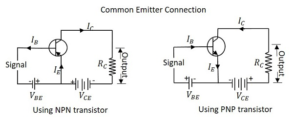
Just as in CB configuration, the emitter junction is forward biased and the collector junction is reverse biased. The flow of electrons is controlled in the same manner. The input current is the base current IB and the output current is the collector current IC here.
Base Current Amplification factor β
The ratio of change in collector current ΔIC to the change in base current ΔIB is known as Base Current Amplification Factor. It is denoted by β
β=ΔICΔ/IB
Relation between β and α
Let us try to derive the relation between base current amplification factor and emitter current amplification factor.
β=ΔIC/ΔIB α=ΔIC/ΔIE IE=IB+IC ΔIE=ΔIB+ΔIC ΔIB=ΔIE−ΔIC We can write β=ΔIC/ΔIE−ΔIC Dividing by ΔIE
β=ΔIC/ΔIE/ΔIE/ΔIE−ΔIC/ΔIE We have α=ΔIC/ΔIE Therefore, β=α/1−α
|
From the above equation, it is evident that, as α approach 1, β reaches infinity.
Hence, the current gain in Common Emitter connection is very high. This is the reason this circuit connection is mostly used in all transistor applications.
Expression for Collector Current
In the Common Emitter configuration, IB is the input current and IC is the output current.
We know
IE=IB+IC And IC=αIE+ICBO =α (IB+IC) +ICBO IC (1−α) =αIB+ICBO IC=α/1−α IB+1/1−α ICBO |
If base circuit is open, i.e. if IB = 0,
The collector emitter current with base open is ICEO
ICEO=1/1−αICBO
Substituting the value of this in the previous equation, we get
IC=α/1−α. IB+ ICEO
IC=βIB+ICEO
Hence the equation for collector current is obtained.
Knee Voltage:
In CE configuration, by keeping the base current IB constant, if VCE is varied, IC increases nearly to 1v of VCE and stays constant thereafter. This value of VCE up to which collector current IC changes with VCE is called the Knee Voltage. The transistors while operating in CE configuration, they are operated above this knee voltage.
Characteristics of CE Configuration
- This configuration provides good current gain and voltage gain.
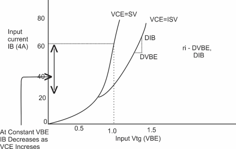
- Keeping VCE constant, with a small increase in VBE the base current IB increases rapidly than in CB configurations.
- For any value of VCE above knee voltage, IC is approximately equal to βIB.
- The input resistance ri is the ratio of change in base emitter voltage ΔVBE to the change in base current ΔIB at constant collector emitter voltage VCE.
ri=ΔVBE/ΔIB at constant VCE
- As the input resistance is of very low value, a small value of VBE is enough to produce a large current flow of base current IB.
- The output resistance ro is the ratio of change in collector emitter voltage ΔVCE to the change in collector current ΔIC at constant IB.
ro=ΔVCE/ΔIC at constant IB
- As the output resistance of CE circuit is less than that of CB circuit.
- This configuration is usually used for bias stabilization methods and audio frequency applications.
Common Collector CC Configuration
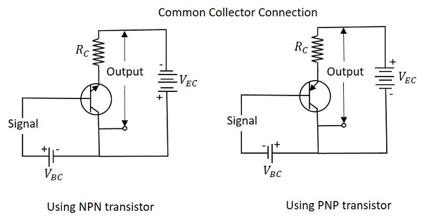
The name itself implies that the Collector terminal is taken as common terminal for both input and output of the transistor. The common collector connection for both NPN and PNP transistors is as shown in the following figure.
|
Just as in CB and CE configurations, the emitter junction is forward biased and the collector junction is reverse biased. The flow of electrons is controlled in the same manner. The input current is the base current IB and the output current is the emitter current IE here.
Current Amplification Factor γ
The ratio of change in emitter current ΔIE to the change in base current ΔIB is known as Current Amplification factor in common collector CC configuration. It is denoted by γ.
γ=ΔIE/ΔIB
- The current gain in CC configuration is same as in CE configuration.
- The voltage gain in CC configuration is always less than 1.
Relation between γ and α
Let us try to draw some relation between γ and α γ=ΔIE/ΔIB α=ΔIC/ΔIE IE=IB+IC ΔIE=ΔIB+ΔIC ΔIB=ΔIE−ΔIC Substituting the value of IB, we get γ=ΔIE/ΔIE−ΔIC Dividing by ΔIEΔIE γ=ΔIE/ΔIE/ΔIE/ΔIE−ΔIC/ΔIE 1/1−α1 γ=1/1−α Expression for collector current We know IC=αIE+ICBO=αIE+ICBO IE=IB+IC=IB+ (αIE+ICBO) IE=IB+IC=IB+ (αIE+ICBO) IE (1−α) =IB+ICBOIE (1−α) =IB+ICBO IE=IB1−α+ICBO1−αIE=IB1−α+ICBO1−α IC≅IE= (β+1) IB+ (β+1) ICBO |
The above is the expression for collector current.
Characteristics of CC Configuration
- This configuration provides current gain but no voltage gains.
- In CC configuration, the input resistance is high and the output resistance is low.
- The voltage gain provided by this circuit is less than 1.
- The sum of collector current and base current equals emitter current.
- The input and output signals are in phase.
- This configuration works as non-inverting amplifier output.
- This circuit is mostly used for impedance matching. That means to drive a low impedance load from a high impedance source.
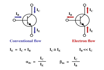
Transistor Current: -
|
Transistor’s Characteristic’s and parameters: -
-The transistors is connected to d.c bias vtg for both the npn & pnp types VBB forward biases the base emitter junction &Vcc reverse biases the base collector junction.
|
*Biasing conditions for different regions of operation: -
Sr. no | Region of operation | BE junction | CB junction | work |
1 | Cutoff region | R.B | R.B | S/w |
2 | Active region | F.B | R.B | Amp |
3 | Saturation region | F.B | F.B |
|
Transistor’s Configuration: -
1) Common Base configuration (C.B)
2) Common emitter Configuration (C.E)
3) Common Collector Configuration (C.C)
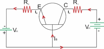
Common Base configuration (C.B):-
|
The I/p is applied between the emitter and the base. The base acts as a common terminal between the I/p and o/p.
-The input vtg is therefore VEB and the input current is IE.
-The output is taken between the collector and the base therefore the output vtg is VCB and the output current is IC.
* Current relation’s in CB configuration:-
-The collector current is IC of the common base configuration is given by
IC = IC (INI) +ICBO
-Where the Ic (INI) called the injected collectors current and it is due to the number of electrons crossing the collectors base junction.
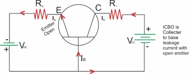
-ICBO: - This is the reverse saturation current flowing due to the minority carrier’s between the collector and base when the emitter is open
-ICBO flow’s due to the reverse biased collector’s base junction. As ICBO negligible as compared to Ic (INI) we can neglect it in practice.
.’. IC=Ic (INI)………………………practically
Ic=ICBO………………with emitter open
|
 Emitter is open
 ICBO
ICBO
Collector is to base control
-Since the ICBO flow’s due to terminally generated minority carrier’s it increases with increase the temperature.
-It doubles its value for every 100c rise in temperature.
-Current amplification factor or current gain: -
Current amplification factor or current gain is the ratio of collector current due to the injection to the total emitter current
αd.c = Ic (INI)
-The value of the ddc for CB configuration will always be less than 1. This is because
IC (INI) < IE.
-Typically the value of d.d.c ranges between them 0.95 to 0.995. Depending upon the thickness of the base region.
-Larger the thickness of the base region smaller the value of the d.d.c
Ic (INI) =d.d.c.IE
Hence the expression for IC is given by
IC=αd.c IE + ICBo--------------------I
But the ICBo is negligibly small
IC d.d.c IE
* Expression for IB:-
IE=IB+IC
IE=αd.cIE+ICBo+IB…………………from I
IB=(1-αd.c)IE-ICBo
Neglecting ICBo
IB= (1-αd.c) IE
- Characteristics of a transistors in a common base configuration: -
1. Input Characteristic: -
A. Input Characteristic: is always a graph of input current verses input vtg. For common base (CB) configuration input current is the emitter current (IE) & I/p vtg. Is the emitter to the base vtg (VEB)
The I/p Characteristic is plotted at a constant O/p vtg. VCB
|
B. Output Characteristic:
Output Characteristic is always a graph of O/p current versus O/p Vtg.
For the CB configuration the O/p current is collector current (IC) of the output voltage is collector to base vtg. (VCB)
Output Characteristic is plotted for a constant value of me /p current (IE)
|
O/p Characteristic of an n-p-n transistor in CB Configuration
Dynamic O/p resistance
Ro =  / I
/ I  constant
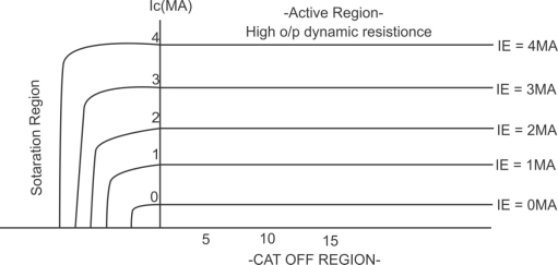
In the active region Ic does not depend on VCB. It depends only on the I/p current IE. That is why the transistor is called as a current controlled or current operated device.
Feature of CB configuration:
- Common terminal : base
- Input current : IE
- O/p current IC
- I/P Vtg. : VEB
- O/P Vtg. VCB
- Current gain :
 ( less than 1)
 - Vtg. Gain : medium
- Input resistance : very low (20-)
- O/P resistance : very high (1 m-2)
- Application : as preamplifier
A digital system understands positional number system where there are few symbols called digits and this symbol represents different values depending on their position in the number.
A value of the digit is determined by using
- The digit
- Its position
- The base of the number system
Decimal Number System
- It’s the system that we use in our daily life. It has a base 10 and uses 10 digits from 0 to 9.
- Here, the successive positions towards the left of the decimal point represent units, tens, hundreds, thousands and so on.
- Each and every position represents a specific power of the base (10). For example, the decimal number 4321 consists of the digit 1 in the units position, 2 in the tens position, 3 in the hundreds position, and 4 in the thousands position, and its value can be written as
(1×1000) + (2×100) + (3×10) + (4×l)
(1×10³) + (2×10²) + (3×101) + (4×l00)
1000 + 200 + 30 + 1
1234
- As a computer programmer, we should understand the following number systems used in computers.
S.N. | Number System & Description |
1 | Binary Number System Base 2. Digits used: 0 and 1 |
2 | Octal Number System Base 8. Digits used: 0 to 7 |
3 | Hex Decimal Number System Base 16. Digits used: 0 to 9, Letters used: A- F |
Binary Number System
- It uses two digits 0 and 1.
- It is also called as base 2 number system.
- Here, each position in any binary number represents a power of the base (2). Example: 23
- The last position represents a y power of the base (2). Example: 2y where y represents the last position.
Decimal-to-Binary conversion
Example
- Binary Number: 101112
Calculating the Decimal Equivalent of binary number −
Step | Binary Number | Decimal Number |
Step 1 | 101012 | ((1 × 24) + (0 × 23) + (1 × 22) + (1 × 21) + (1 × 20))10 |
Step 2 | 101012 | (16 + 0 + 4 + 2 + 1)10 |
Step 3 | 101012 | 2310 |
Note: 101112 are normally written as 10111.
2. Decimal Number: 2710
Calculating Binary Equivalent −
Step | Operation | Result | Remainder |
Step 1 | 27 / 2 | 13 | 1 |
Step 2 | 13 / 2 | 6 | 1 |
Step 3 | 6 / 2 | 3 | 0 |
Step 4 | 3 / 2 | 1 | 1 |
Step 5 | 1 / 2 | 0 | 1 |
Hence, the remainders are arranged in the reverse order and we get:
Decimal Number − 2710 = Binary Number − 110112.
Simple binary arithmetic
It is an essential part of all the digital calculations.
Binary Addition
- It is a basis for binary subtraction, multiplication, division.
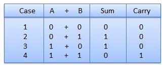
- There are four rules which are as follows:
|
Fig: Rules of Binary addition
In fourth step, a sum (1 + 1 = 10) i.e. 0 is written in the given column and a carry of 1 over to the next column is done.
For Example −
|
Fig: Binary addition
Binary Subtraction
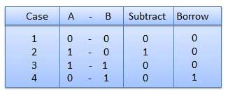
Subtraction and Borrow, these are the two words that will be used very frequently for binary subtraction. There rules of binary subtraction are:
|
Fig. Rules of Binary Subtraction
For Example
|
Fig. Binary subtraction
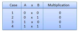
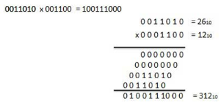
Binary Multiplication
- It is similar to decimal multiplication.
- It is also simpler than decimal multiplication as only 0s and 1s are involved.
- There are four rules of binary multiplication which are:
|
Fig. Rules of Binary Multiplication (Ref. 1)
For Example
|
Fig. Binary Multiplication
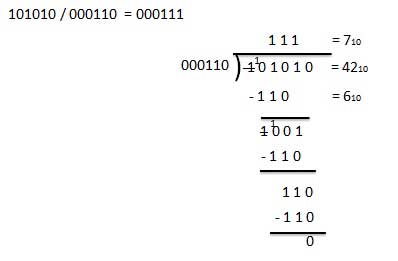
Binary Division
- It is similar to decimal division.
- It is also called as the long division procedure.
For Example
|
Fig. Binary Division
Logic Gates
The basic gates are namely AND gate, OR gate & NOT gate.
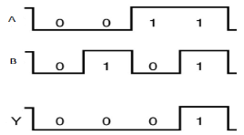
AND gate
It is a digital circuit that consists of two or more inputs and a single output which is the logical AND of all those inputs. It is represented with the symbol ‘.’.
The following is the truth table of 2-input AND gate.
A | B | Y = A.B |
0 | 0 | 0 |
0 | 1 | 0 |
1 | 0 | 0 |
1 | 1 | 1 |
Here A, B are the inputs and Y is the output of two input AND gate.
If both inputs are ‘1’, then only the output, Y is ‘1’. For remaining combinations of inputs, the output, Y is ‘0’.
The figure below shows the symbol of an AND gate, which is having two inputs A, B and one output, Y.
|
Fig. : AND gate (ref. 1)
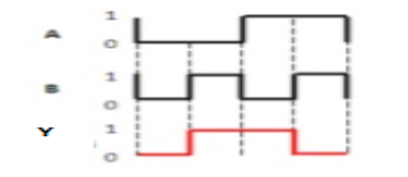
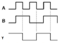
Timing Diagram:
|
OR gate
It is a digital circuit which has two or more inputs and a single output which is the logical OR of all those inputs. It is represented with the symbol ‘+’.
The truth table of 2-input OR gate is:
A | B | Y = A + B |
0 | 0 | 0 |
0 | 1 | 1 |
1 | 0 | 1 |
1 | 1 | 1 |
Here A, B are the inputs and Y is the output of two input OR gate.
When both inputs are ‘0’, then only the output, Y is ‘0’. For remaining combinations of inputs, the output, Y is ‘1’.
The figure below shows the symbol of an OR gate, which is having two inputs A, B and one output, Y.
|
Fig. : OR gate (ref. 1)
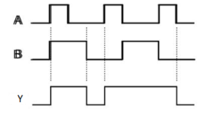
Timing Diagram:
|
NOT gate
It is a digital circuit that has one input and one output. Here the output is the logical inversion of input. Hence, it is also called as an inverter.
The truth table of NOT gate is:
A | Y = A’ |
0 | 1 |
1 | 0 |
Here A and Y are the corresponding input and output of NOT gate. When A is ‘0’, then, Y is ‘1’. Similarly, when, A is ‘1’, then, Y is ‘0’.
The figure below shows the symbol of NOT gate, which has one input, A and one output, Y.
|
Fig. : NOT gate (ref. 1)
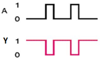
Timing Diagram:
|
The NAND NOR, Exclusive-OR and Exclusive-NOR gate
NAND gate
It is a digital circuit which has two or more inputs and single output and it is the inversion of logical AND gate.
The truth table of 2-input NAND gate is:
A | B | Y = (A.B)’ |
0 | 0 | 1 |
0 | 1 | 1 |
1 | 0 | 1 |
1 | 1 | 0 |
Here A, B are the inputs and Y is the output of two input NAND gate. When both inputs are ‘1’, then the output, Y is ‘0’. If at least one of the inputs is zero, then the output, Y is ‘1’. This is just the inverse of AND operation.
The image shows the symbol of NAND gate:
|
Fig.: NAND gate (ref. 1)
NAND gate works same as AND gate followed by an inverter.
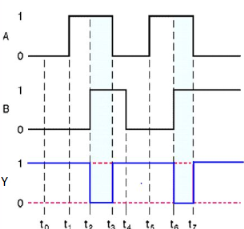
Timing Diagram:
|
NOR gate
It is a digital circuit that has two or more inputs and a single output which is the inversion of logical OR of all inputs.
The truth table of 2-input NOR gate is:
A | B | Y = (A+B)’ |
0 | 0 | 1 |
0 | 1 | 0 |
1 | 0 | 0 |
1 | 1 | 0 |
Here A and B are the two inputs and Y is the output. If both inputs are ‘0’, then the output is ‘1’. If any one of the inputs is ‘1’, then the output is ‘0’. This is exactly opposite to two input OR gate operation.
The symbol of NOR gate is:
|
Fig.: NOR gate (ref. 1)
NOR gate works exactly same as that of OR gate followed by an inverter.
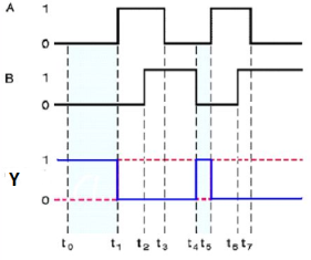
Timing Diagram:
|
Special Gates
Ex-OR gate
It stands for Exclusive-OR gate. Its function varies when the inputs have even number of ones.
The truth table of 2-input Ex-OR gate is:
A | B | Y = A⊕B |
0 | 0 | 0 |
0 | 1 | 1 |
1 | 0 | 1 |
1 | 1 | 0 |
Here A, B are the inputs and Y is the output of two input Ex-OR gate. The output (Y) is zero instead of one when both the inputs are one.
Therefore, the output of Ex-OR gate is ‘1’, when only one of the two inputs is ‘1’. And it is zero, when both inputs are same.
The symbol of Ex-OR gate is as follows:
|
Fig.: XOR gate (ref. 1)
It is similar to that of OR gate with an exception for few combination(s) of inputs. Hence, the output is also known as an odd function.
Timing Diagram:
|
Ex-NOR gate
It stands for Exclusive-NOR gate. Its function neither is same as that of NOR gate except when the inputs having even number of ones.
The truth table of 2-input Ex-NOR gate is:
A | B | Y = A⊙B |
0 | 0 | 1 |
0 | 1 | 0 |
1 | 0 | 0 |
1 | 1 | 1 |
Here A, B are the inputs and Y is the output. It is same as Ex-NOR gate with the only modification in the fourth row. The output is 1 instead of 0, when both the inputs are one.
Hence the output of Ex-NOR gate is ‘1’, when both inputs are same and 0, when both the inputs are different.
The symbol of Ex-NOR gate is:
|
Fig.: XNOR gate (ref. 1)
It neither is similar to NOR gate except for few combination of inputs. Here the output is ‘1’, when even number of 1 is present at the inputs. Hence is also called as an even function.
Timing Diagram:
|
- It deals with binary numbers & variables.
- Therefore, also known as Binary Algebra or logical Algebra.
- A mathematician named as George Boole had developed this algebra in 1854.
- The variables that are used in this algebra are known as Boolean variables.
- Considering the range of voltages as logic ‘High’ is represented with ‘1’ and logic ‘Low’ is represented with ‘0’.
Postulates and Basic Laws of Boolean algebra
Here, the Boolean postulates and basic laws that are used are given underneath.
Boolean Postulates
- Considering the binary numbers 0 and 1, Boolean variable (x) and its complement (x’).
- They know as literal.
- The possible logical OR operations are:
x + 0 = x
x + 1 = 1
x + x = x
x + x’ = 1
- Similarly, the possible logical AND operations are:
x.1 = x
x.0 = 0
x.x = x
x.x’ = 0
- These are the simple Boolean postulates and verification can be done by substituting the Boolean variable with ‘0’ or ‘1’.
Laws and Rules of Boolean algebra
Basic Laws of Boolean algebra
- The three basic laws of Boolean Algebra are:
- Commutative law
- Associative law
- Distributive law
Commutative Law
- The logical operation carried between two Boolean variables when gives the same result irrespective of the order the two variables, then that operation is said to be Commutative. The logical OR & logical AND operations between x & y are shown below
x + y = y + x
x.y=y.x
- The symbol ‘+’ and ‘.’ indicates logical OR operation and logical AND operation.
- Commutative law holds logical OR & logical AND operations.
Associative Law
- If a logical OR operation of any two Boolean variables is performed first and then the same operation is performed with the remaining variable providing the same result, then that operation is said to be Associative. The logical OR & logical AND operations of x, y & z are:
x + (y + z) = (x + y) + z
x. (y.x) = (x.y).z
- Associative law holds well for logical OR & logical AND operations.
Distributive Law
- If a logical OR operation of any two Boolean variables is performed first and then AND operation is performed with the remaining variable, then that logical operation is said to be Distributive. The distribution of logical OR & logical AND operations between variables x, y & z are :
x. (y + z) = x.y + x.z
x + (y.x) = (x + y). (x + z)
- Distributive law holds well for logical OR and logical AND operations.
- These are the Basic laws of Boolean algebra and we can verify them by substituting the Boolean variables with ‘0’ or ‘1’.
Numerical
- Simplify the Boolean function,
f = p’qr + pq’r + pqr’ + pqr
Method 1
Given
f = p’qr + pq’r + pqr’ +pqr.
In first and second term r is common and in third and fourth terms pq is common.
So, taking out the common terms by using Distributive law we get,
⇒ f = (p’q + pq’) r + pq (r’ + r)
The terms present in first parenthesis can be simplified by using Ex-OR operation.
The terms present in second parenthesis is equal to ‘1’ using Boolean postulate we get
⇒ f = (p ⊕q) r + Pq (1)
The first term can’t be simplified further.
But, the second term is equal to pq using Boolean postulate.
⇒ f = (p ⊕q) r + pq
Therefore, the simplified Boolean function is f = (p⊕q) r + pq
Method 2
Given f = p’qr + pq’r + pqr’ + pqr.
Using the Boolean postulate, x + x = x.
Hence we can write the last term pqr two more times.
⇒ f = p’qr + pq’r + pqr’ + pqr + pqr + pqr
Now using the Distributive law for 1st and 4th terms, 2nd and 5th terms, 3rdand 6th terms we get.
⇒ f = qr (p’ + p) + pr (q’ + q) + pq (r’ + r)
Using Boolean postulate, x + x’ = 1 and x.1 = x for further simplification.
⇒ f = qr (1) + pr (1) + pq (1)
⇒ f = qr + pr + pq
⇒ f = pq + qr + pr
Therefore, the simplified Boolean function is f = pq + qr + pr.
Hence we got two different Boolean functions after simplification of the given Boolean function. Functionally, these two functions are same. As per requirement, we can choose one of them.
Numerical
Find the complement of the Boolean function,
f = p’q + pq’.
Solution:
Using Demerger’s theorem, (x + y)’ = x’.y’ we get
⇒ f’ = (p’q)’.(pq’)’
Then by second law, (x.y)’ = x’ + y’ we get
⇒ f’ = {(p’)’ + q’}. {p’ + (q’)’}
Then by using, (x’)’=x we get
⇒ f’ = {p + q’}. {p’ + q}
⇒ f’ = pp’ + pq + p’q’ + qq’
Using x.x’=0 we get
⇒ f = 0 + pq + p’q’ + 0
⇒ f = pq + p’q’
Therefore, the complement of Boolean function, p’q + pq’ is pq + p’q’.
Standard forms of Boolean expressions
- Four product combinations is obtained by combining two variables x and y with logical AND operation. They are called as min terms or standard product terms. The min terms are given as x’y’, x’y, xy’ and xy.
- In the same way, four Boolean sum terms is obtained by combining two variables x and y with logical OR operation. They are called as Max terms or standard sum terms. The Max terms are given as x + y, x + y’, x’ + y and x’ + y’.
The following table represents the min terms and MAX terms for 2 variables.
x | y | Min terms | Max terms |
0 | 0 | m0=x’y’ | M0=x + y |
0 | 1 | m1=x’y | M1=x + y’ |
1 | 0 | m2=xy’ | M2=x’ + y |
1 | 1 | m3=xy | M3=x’ + y’ |
- If the binary variable is ‘0’, then it is represented as complement of variable in min term and as the variable itself in Max term.
- Similarly, if it is ‘1’, then it is represented as complement of variable in Max term and as the variable itself in min term.
- From the above table, we can easily notice that min terms and Max terms are complement of each other.
- If there are ‘n’ Boolean variables, then there will be 2n min terms and 2n Max terms.
Canonical SoP and PoS forms
- A truth table comprises of a set of inputs and output(s).
- If there are ‘n’ input variables, then there shall be 2n possible combinations comprising of zeros and ones.
- So the value of every output variable depends on the combination of input variables.
- Hence, each output variable has ‘1’ for some combination and ‘0’ for other combination of input variables.
Therefore, we can express each output variable in two ways.
- Canonical SoP form
- Canonical PoS form
Canonical SoP form
- It means Canonical Sum of Products form.
- In this, each product term contains all literals.
- So that these product terms are nothing but the min terms.
- Hence is also known as sum of min terms form.
- Firstly, identification of the min terms is done and then the logical OR of those min terms is taken in order to get the Boolean expression (function) corresponding to that output variable.
- This Boolean function will be in sum of min terms form.
- Then following the same procedure for other output variables too.
Example
Consider the following truth table.
Inputs | Output | ||
P | q | r | f |
0 | 0 | 0 | 0 |
0 | 0 | 1 | 0 |
0 | 1 | 0 | 0 |
0 | 1 | 1 | 1 |
1 | 0 | 0 | 0 |
1 | 0 | 1 | 1 |
1 | 1 | 0 | 1 |
1 | 1 | 1 | 1 |
- Here, the output (f) is ‘1’ for only four combinations of inputs.
- The corresponding min terms are given as p’qr, pq’r, pqr’, pqr.
- By doing logical OR, we get the Boolean function of output (f).
- Hence, the Boolean function of output is,
f = p’qr + pq’r + pqr’ + pqr.
- This is the desired canonical SoP form of output, f.
- It can also be represented as:
f=m3+m5+m6+m7f=m3+m5+m6+m7
f=∑m (3, 5, 6, 7) f=∑m (3, 5, 6, 7)
- First, we represented the function as sum of respective min terms and then, the symbol for summation of those min terms is used.
Canonical PoS form
- It means Canonical Product of Sums form.
- Here In this form, each sum term contains all literals.
- These sum terms are the Max terms.
- Hence, canonical PoS form is also known as product of Max terms form.
- Identification of the Max terms for which the output variable is zero is done and then the logical AND of those Max terms is done in order to get the Boolean expression corresponding to that output variable.
- This Boolean function is in the form of product of Max terms.
- Following the same procedure for other output variables too.
Standard SoP and PoS forms
Standard SoP form
- It stands for Standard Sum of Products form.
- In this, each product term need not contain all literals.
- So, the product terms can or cannot be the min terms.
- Therefore, it is therefore the simplified form of canonical SoP form.
Standard SoP of output variable can be obtained by two steps.
- Getting the canonical SoP form of output variable
- Simplification the above Boolean function.
The same procedure is followed for other output variables too, if there is more than one output variable.
Numerical
Convert the Boolean function into Standard SoP form.
f = p’qr + pq’r + pqr’ + pqr
Solution:
Step 1 – By using the Boolean postulate, x + x = x and also writing the last term pqr two more times we get
⇒ f = p’qr + pq’r + pqr’ + pqr + pqr + pqr
Step 2 – By Using Distributive law for 1st and 4th terms, 2nd and 5th terms, 3rdand 6th terms.
⇒ f = qr (p’ + p) + pr (q’ + q) + pq (r’ + r)
Step 3 – Then Using Boolean postulate, x + x’ = 1 we get
⇒ f = qr (1) + pr (1) + pq (1)
Step 4 – hence using Boolean postulate, x.1 = x we get
⇒ f = qr + pr + pq
⇒ f = pq + qr + pr
This is the required Boolean function.
Standard PoS form
- It stands for Standard Product of Sum form.
- Here, each sum term need not contain all literals.
- So, the sum terms can or cannot be the Max terms.
- Therefore, it is the desired simplified form of canonical PoS form.
Standard PoS form of output variable is obtained by two steps.
- Getting the canonical PoS form of output variable
- Simplification of the above Boolean function.
The same procedure is followed for other output variables too.
Numerical
Convert the Boolean function into Standard PoS form.
f = (p + q + r). (p + q + r’). (p + q’ + r). (p’ + q + r)
Solution:
Step 1 – By using the Boolean postulate, x.x = x and writing the first term p+q+r two more times we get
⇒ f = (p + q + r). (p + q + r). (p + q + r). (p + q + r’). (p +q’ + r). (p’ + q + r)
Step 2 – Now by using Distributive law, x + (y.x) = (x + y). (x + z) for 1st and 4thparenthesis, 2nd and 5th parenthesis, 3rd and 6th parenthesis.
⇒ f = (p + q + rr’). (p + r + qq’). (q + r + pp’)
Step 3 − Applying Boolean postulate, x.x’=0 for simplifying of the terms present in each parenthesis.
⇒ f = (p + q + 0). (p + r + 0). (q + r + 0)
Step 4 − Using Boolean postulate, x + 0 = x we get
⇒ f = (p + q). (p + r). (q + r)
⇒ f = (p + q). (q + r). (p + r)
This is the simplified Boolean function.
Hence, both Standard SoP and Standard PoS forms are Dual to one another.
- Karnaugh map method or K-map method is the pictorial representation of the Boolean equations and Boolean manipulations are used to reduce the complexity in solving them. These can be considered as a special or extended version of the ‘Truth table’.
- Karnaugh map can be explained as “An array containing 2k cells in a grid like format, where k is the number of variables in the Boolean expression that is to be reduced or optimized”. As it is evaluated from the truth table method, each cell in the K-map will represent a single row of the truth table and a cell is represented by a square.
- The cells in the k-map are arranged in such a way that there are conjunctions, which differ in a single variable, are assigned in adjacent rows. The K-map method supports the elimination of potential race conditions and permits the rapid identification.
- By using Karnaugh map technique, we can reduce the Boolean expression containing any number of variables, such as 2-variable Boolean expression, 3-variable Boolean expression, 4-variable Boolean expression and even 7-variable Boolean expressions, which are complex to solve by using regular Boolean theorems and laws.
- Minimization with Karnaugh Maps and advantages of K-map:
- K-maps are used to convert the truth table of a Boolean equation into minimized SOP form.
- Easy and simple basic rules for the simplification.
- The K-map method is faster and more efficient than other simplification techniques of Boolean algebra.
- All rows in the K-map are represented by using square shaped cells, in which each square in that will represent a minterms.
- It is easy to convert a truth table to k-map and k-map to Sum of Products form equation.
There are 2 forms in converting a Boolean equation into K-map:
Un-optimized form
Optimized form
- Un-optimized form: It involves in converting the number of 1’s into equal number of product terms (min terms) in an SOP equation.
- Optimized form: It involves in reducing the number of min terms in the SOP equation.
Grouping of K-map variables
- There are some rules to follow while we are grouping the variables in K-maps. They are
- The square that contains ‘1’ should be taken in simplifying, at least once.
- The square that contains ‘1’ can be considered as many times as the grouping is possible with it.
- Group shouldn’t include any zeros (0).
- A group should be the as large as possible.
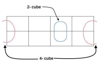
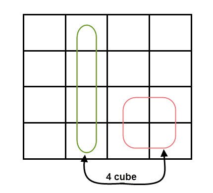
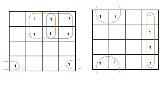
- Groups can be horizontal or vertical. Grouping of variables in diagonal manner is not allowed.
|
- If the square containing ‘1’ has no possibility to be placed in a group, then it should be added to the final expression.
- Groups can overlap.
- The number of squares in a group must be equal to powers of 2, such as 1, 2, 4, 8 etc.
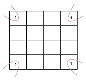
- Groups can wrap around. As the K-map is considered as spherical or folded, the squares at the corners (which are at the end of the column or row) should be considered as they adjacent squares.
- The grouping of K-map variables can be done in many ways, so they obtained simplified equation need not to be unique always.
- The Boolean equation must be in must be in canonical form, in order to draw a K-map.
|
2 variable K-maps
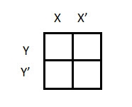
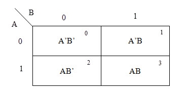
There are 4 cells (22) in the 2-variable k-map. It will look like (see below image)
|
The possible min terms with 2 variables (A and B) are A.B, A.B’, A’.B and A’.B’. The conjunctions of the variables (A, B) and (A’, B) are represented in the cells of the top row and (A, B’) and (A’, B’) in cells of the bottom row. The following table shows the positions of all the possible outputs of 2-variable Boolean function on a K-map.
|
A general representation of a 2 variable K-map plot is shown below.
|
When we are simplifying a Boolean equation using Karnaugh map, we represent each cell of K-map containing the conjunction term with 1. After that, we group the adjacent cells with possible sizes as 2 or 4. In case of larger k-maps, we can group the variables in larger sizes like 8 or 16.
The groups of variables should be in rectangular shape that means the groups must be formed by combining adjacent cells either vertically or horizontally. Diagonal shaped or L-shaped groups are not allowed. The following example demonstrates a K-map simplification of a 2-variable Boolean equation.
Example
Simplify the given 2-variable Boolean equation by using K-map.
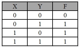
F = X Y’ + X’ Y + X’Y’
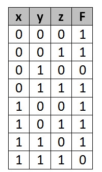
First, let’s construct the truth table for the given equation,
|
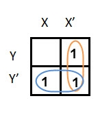
We put 1 at the output terms given in equation.
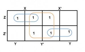
|
In this K-map, we can create 2 groups by following the rules for grouping, one is by combining (X’, Y) and (X’, Y’) terms and the other is by combining (X, Y’) and (X’, Y’) terms. Here the lower right cell is used in both groups.
After grouping the variables, the next step is determining the minimized expression.
By reducing each group, we obtain a conjunction of the minimized expression such as by taking out the common terms from two groups, i.e. X’ and Y’. So the reduced equation will be X’ +Y’.
3 variable K-maps
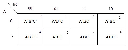
For a 3-variable Boolean function, there is a possibility of 8 output min terms. The general representation of all the min terms using 3-variables is shown below.
|
A typical plot of a 3-variable K-map is shown below. It can be observed that the positions of columns 10 and 11 are interchanged so that there is only change in one variable across adjacent cells. This modification will allow in minimizing the logic.
|
Up to 8 cells can be grouped in case of a 3-variable K-map with other possibilities being 1, 2 and 4.
Example
Simplify the given 3-variable Boolean equation by using k-map.
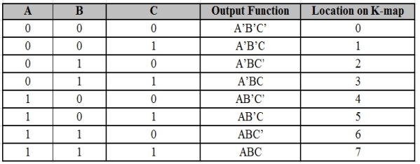
F = X’ Y Z + X’ Y’ Z + X Y Z’ + X’ Y’ Z’ + X Y Z + X Y’ Z’
First, let’s construct the truth table for the given equation,
|
We put 1 at the output terms given in equation.
There are 8 cells (23) in the 3-variable k-map. It will look like (see below image).
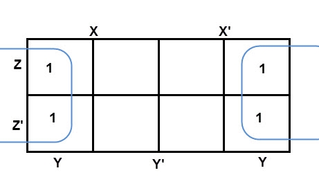
The largest group size will be 8 but we can also form the groups of size 4 and size 2, by possibility. In the 3 variable Karnaugh map, we consider the left most column of the k-map as the adjacent column of rightmost column. So the size 4 group is formed as shown below.
|
And in both the terms, we have ‘Y’ in common. So the group of size 4 is reduced as the conjunction Y. To consume every cell which has 1 in it, we group the rest of cells to form size 2 group, as shown below.
|
The 2 size group has no common variables, so they are written with their variables and its conjugates. So the reduced equation will be X Z’ + Y’ + X’ Z. In this equation, no further minimization is possible.
4 variable K-maps
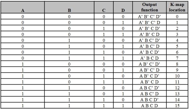
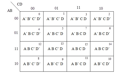
There are 16 possible min terms in case of a 4-variable Boolean function. The general representation of minterms using 4 variables is shown below.
|
A typical 4-variable K-map plot is shown below. It can be observed that both the columns and rows of 10 and 11 are interchanged.
|
The possible numbers of cells that can be grouped together are 1, 2, 4, 8 and 16.
Example
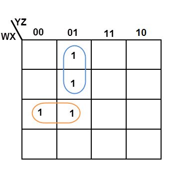
Simplify the given 4-variable Boolean equation by using k-map. F (W, X, Y, Z) = (1, 5, 12, 13)
Sol: F (W, X, Y, Z) = (1, 5, 12, 13)
|
By preparing k-map, we can minimize the given Boolean equation as
F = W Y’ Z + W ‘Y’ Z
5 variable K-maps
A 5-variable Boolean function can have a maximum of 32 minterms. All the possible minterms are represented below
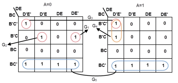
In 5-variable K-map, we have 32 cells as shown below. It is represented by F (A, B, C, D, and E). It is divided into two grids of 16 cells with one variable (A) being 0 in one grid and 1 in other grid.
|
Example
Simplify the given 5-variable Boolean equation by using k-map.
f (A, B, C, D, E) = ∑ m (0, 5, 6, 8, 9, 10, 11, 16, 20, 42, 25, 26, 27)
|
K-map with “Don’t care” conditions
The “Don’t care” conditions are used to replace the empty cell to form a possible grouping of variables. They can be used as either 0 or 1, based on the adjacent variables in the group. The cells that contain “don’t care” conditions are represented by an asterisk (*) symbol among the normal 0’s and 1’s.
In grouping of variables, we can also ignore the “don’t cares”. “Don’t care” conditions are very useful in grouping the variables of large size.
Minimizing an Expression with Don’t Cares
We can minimize the Boolean expression by finding the relative functions of the ‘don’t care’ conditions, by assigning them 0 or 1. If n is the number of don’t cares in a Boolean equation, the number of functions obtained will be 2n.
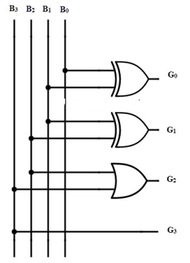
Implementation of BCD to Gray Code Converter using K-map
A Gray code is a number series in which two successive numbers differ by one bit. This code acquired its name by the scientist “Frank Gray”. He owned the patent for using the Gray code in shaft registers, in the year of 1953.
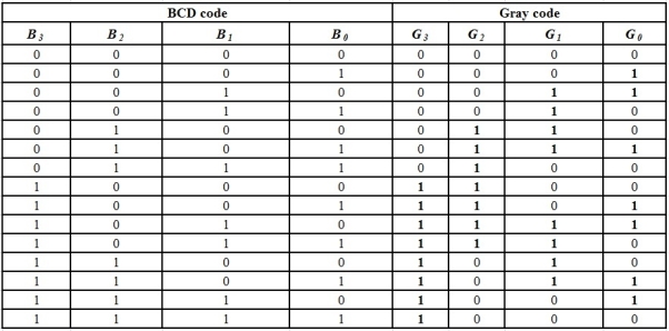
We can convert the binary coded decimal (BCD) code to Gray code by using k-map simplification.
Table for BCD code and Gray code
|
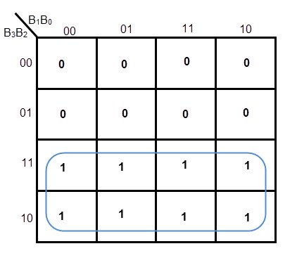
K-MAP FOR G3
|
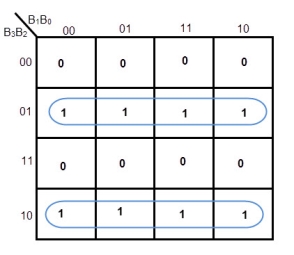
K-MAP FOR G2
Equation for G2= B3’ B2 + B3 B2’= B3 XOR B2
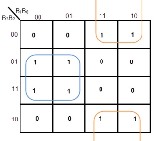
|
K-MAP FOR G1
|
Equation for G1= B1’ B2 + B1 B2’= B1 XOR B2
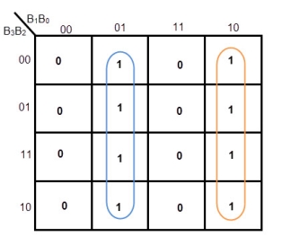
K-MAP FOR G0
|
Equation for G0= B1’ B0 + B1 B0’= B1 XOR B0
The the implementation of BCD to Gray conversion using logic gates is shown below. Two EX-OR gates and an OR gate are used.
|
References:
1. V. Del Toro “ Principles of Electrical Engineering”, Prentice Hall
2. I.J. Nagrath “ Basic Electrical Engineering”, Tata McGraw Hill
3. D.F. Fitzgerald, A. Grabel Higginbotham “ Basic Electrical Engineering”, McGraw Hill
4. Mittal & Mittal “ Basic Electrical Engineering”, Tata McGraw Hill
5. B.L. Theraja and A.K. Theraja“A Text Book of Electrical Technology”, Volume - I & II
6. J. Millman & Halkias “ Electronic Devices & Circuits”, Tata McGraw Hill
7. Herbert Taub “ Digital Circuits & Microprocessors”, McGraw Hill
