MODULE 1
ELECTRONIC MATERIALS
The classical free electron theory of metals (Drude –Lorentz theory of metals) Drude and Lorentz proposed this theory in 1900. According to this theory, the metals containing the free electrons obey the laws of classical mechanics.
Assumptions ( or salient features) in classical free electron theory
The classical free electron theory is based on the following postulates.
1. The valence electrons of atoms are free to move about the whole volume of the metal, like the molecules of a perfect gas in a container.
2. The free electrons move in random direction and collide with either positive ions fixed to the lattice or the other free electrons. All the collisions are elastic in nature i.e., there is no loss of energy.
3. The momentum of free electrons obeys the laws of the classical kinetic theory of gases.
4. The electron velocities in a metal obey classical Maxwell-Boltzman distribution of velocities.
5. When the electric field is applied to the metal, the free electrons are accelerated in the direction opposite to the direction of applied electric field.
6. The mutual repulsion among the electrons is ignored, so that they move in all the directions with all possible velocities.
7. In the absence of the field, the energy associated with an electron at temperature T is given by  kT. It is related to the kinetic energy equation
 kT =
kT =  v2th
v2th
Here vth represents the thermal velocity.
Success of classical free electron theory
1. It verifies ohm’s law
2. It explains electrical conductivity of metals.
3. It explains thermal conductivity of metals.
4. It derives Widemann – Franz law. (i.e. the relation between electrical and thermal conductivity.
Draw backs of classical free electron theory
1. It could not explain the photoelectric effect, Compton Effect and black body radiation.
2. Electrical conductivity of semiconductors and insulators could not be explained.
3. Widemann – Franz law (K/σT= constant) is not applicable at lower temperatures.
4. Ferromagnetism could not be explained by this theory. The theoretical value of paramagnetic susceptibility is greater than the experimental value.
5. According to classical free electron theory the specific heat of metals is given by 4.5R whereas the experimental value is given by 3R.
6. According to classical free electron the electronic specific heat is equal to 3/2R while the actual value is 0.01R.
Electrical Conductivity
The classical free electron theory was proposed by Drude and Lorentz. According to this theory the electrons are moving freely and randomly moving in the entire volume of the metal like gas atoms in the gas container. When an electric field is applied the free electrons gets accelerated.
When an electric field E is applied between the two ends of a metal of area of cross section A
When an electrical field (E) is applied to an electron of charge ‘e’ of a metallic rod, the electron moves in opposite direction to the applied field with a velocity vd. This velocity is known as drift velocity.
Drift velocity vd is defined as the average velocity of the free electrons with which they move towards the positive terminal under the influence of the electrical field.
Lorentz force acting on the electron F = eE ........(1)
This force is known as the driving force of the electron.
Due to this force, the electron gains acceleration ‘a’.
From Newton’s second law of motion,
Force F = ma …....(2)
From the equation (1) and (2),
Ma = eE or
a =  …......(3)
Acceleration (a) = 
Or a = 
Relaxation time is defined as the time taken by a free electron to reach its equilibrium position from the disturbed position in the presence of an electric field.
So vd = a ……….(4)
Substituting equation (3) in (4)
vd =  =
=  E ……….(5)
vd =  E ……….(5a)
Where  = RMS velocity
The Ohms’ law states that current density (J) is expressed as
J =E ……….(6)
Or = 
Where is the electrical conductivity of the electron.
But, the current density in terms of drift velocity is given as
J = nevd ....... (7)
Substituting equation (5) in equation (7), we have
J = ne E
E
Or  =
= 
On comparing the equation (6) and (8) , we have
Electrical conductivity
=  ....... (8)
=  ....... (8a)
This is a required expression for electrical conductivity.
Resistivity ρ
ρ =  =
= 
According to kinetic theory of gasses
 =
= 
So =  =
=
Also
ρ =  =
= 
Mobility: It is defined as the drift velocity of the charge carrier per unit applied electric field.
μ=  ....... (9)
From equation (7) we have
J = nevd
By substituting vd =μE from equation (9)
J = neμE
Or  = μne ....... (10)
We know by ohms law =  so equation (10) can be rewritten as
= μne
μ = 
This is the required expression for mobility.
Temperature Dependence
The positive ions are always in oscillating (or vibrating) state about their mean position; even the substance is present at 0k temperature. The vibrating amplitude of ions is always depends the temperature. The mean free path λ of the electrons is inversely proportional to the mean square of amplitude of ionic vibrations A0
λ =  ………(1)
The energy of lattice vibrations is proportional to  and increases linearly with temperature T.
 T ……….(2)
From equations (1) and (2)
λ =  ………..(3)
The resistivity ρ of the metal is inversely proportional to mean free path of electrons λ
ρ =  ..…………..(4)
From equations (3) and (4)
ρ T ..……….(5)
From equation (5) we observe that the resistivity of metal is linearly increases with temperature. The conductivity is defined as the reciprocal of resistance.

 ………….(6)
From equation (6) we observe that the conductivity of metal is inversely proportional to their temperature. The variation of resistivity of metal with temperature is shown in figure.
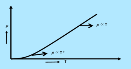
Figure 1
A parameter of interest in the study of conductivity of metals and semiconductors is the density of states.
The Fermi function F(E) gives only the probability of filling up of electrons in a given energy state. It does not give the information about the number of electrons that can be filled in a given energy state, to know that we should know the number of available energy states called density of states.
Density of states is defined the as the number of energy states per unit volume in an energy interval of a metal. It is use to calculate the number of charge carriers per unit volume of any solid.
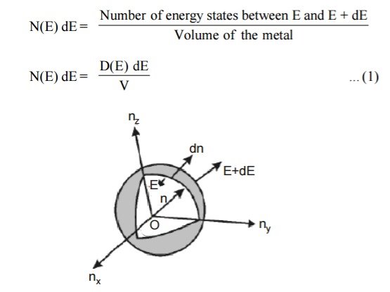
Figure 2: Positive octant of n space
Let us constant a sphere of radius “n” in space with quantum numbers nn , ny and nz

The sphere is further divided into many shells represents a particular combination of quantum numbers and represents particular energy value.
Therefore, the number of energy states within a sphere of radius

Let us consider two energy values E and E + dE can be found by finding the number of energy states between the shells of radius n and n+ dn from the origin. Since the quantum numbers are positive integers, n values can be defined only in the positive octant of the n – space.
The number of available energy states within the sphere of radius “n” due to one octant.

Similarly the number of available energy states within the sphere of radius n+dn corresponding energy.

The number of available energy states between the shells of radius n and n + dn (or) between the energy levels E and E + dE

The number of available energy states between the energy interval dE

Since the higher powers of dn is very small, dn2 and dn3 terms can be neglected.

We know that the allowed energy values is

Differentiating equation (4) with respect to ‘n’
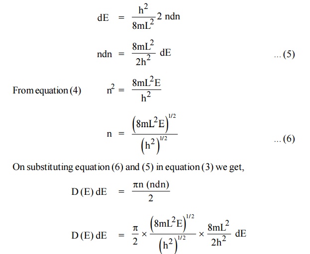
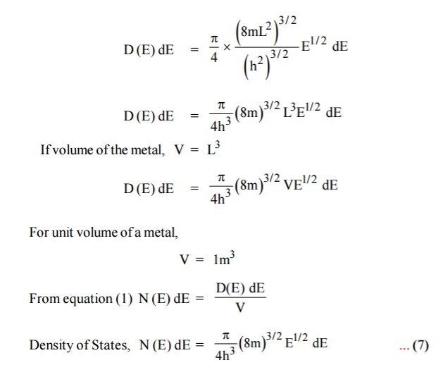
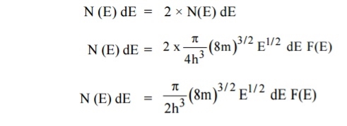
Each electron energy level can accommodate two electrons as per Pauli’s exclusion principle. (Spin up and Spin down = 2 (e) × density of states).
Carrier Concentration In Metals
Let N(E) dE represents the number of filled energy states between the interval of energy dE, normally all the energy states will not be filled
DN = N (E) dE F(E)

Normally all the states are not filled states, filling of electrons is a given energy state is given by Fermi-function F(E). Let dn represents the number of filled energy states.
In this case of material of absolute zero the upper occupied level is EF and for all the levels below EF, F(E)=1 (at T = 0 K the maximum energy level that can be occupied by the electron is called Fermi energy level EF T = 0 K F(E) = 1).
Integrating equation (8) within the limits 0 to EF0 us can get the number of energy states of electron (N)
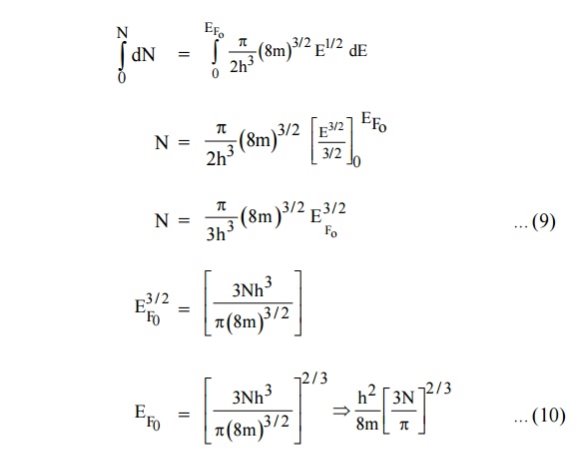
Hence the Fermi energy of a metal depends only on the density of electrons of that metal.
Bands are formed by the closely spaced orbitals.
There are three types of bands:
1. Valance Bands: Valence band it is a group of orbitals which contain electrons in the shell. Or we can say It is also defined as the energy band that comprises of valence electrons present in the outermost shell of an atomic structure.
These valence electrons, when provided with sufficient energy, get changed into free electrons and moves to conduction band thereby causing conductivity. It is at a lower energy level than the conduction band in the energy level diagram.
2. Conduction Band: Conduction band is a group of empty orbitals of the shells that do not contain any electron due to their configuration making the orbitals of higher energy levels.
When the electrons pass from valance band to the conduction band these solids conduct electricity with flow of charges in the form of electrons.
3. Forbidden Energy Band: These two bands are separated by a certain amount of energy known as the forbidden energy gap. In this band not a single electron is available. It diagram it is named as Band Gap.
Let us distinguish between conductor, semiconductors and insulator on the basis of these bands.
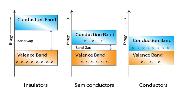
Figure 3
- In Conductors: The valance band and the conduction band overlap each other. This makes it easy for the electricity to pass through them. In conductors, the valence band is either not fully occupied with electrons, or the filled valence band overlaps with the empty conduction band. In general, both states occur at the same time, the electrons can therefore move inside the partially filled valence band or inside the two overlapping bands. In conductors there is no band gap between the valence band and conduction band.
- In Semi-conductors: there is a slight gap between the conduction band and the valance band. This band gap is less than or equal to 1.4 eV. The electrons from valance shell take a little energy to excite from valance band to the conduction band. Even in semiconductors, there is a band gap, but compared to insulators it is so small that even at room temperature electrons from the valence band can be lifted into the conduction band. The electrons can move freely and act as charge carriers.
- In Insulators: In insulators the valence band is fully occupied with electrons due to the covalent bonds. To achieve conductivity, electrons from the valence band have to move into the conduction band. the energy gap is considerably large and the electrons of the valance band cannot be excited to the conduction band before the melting or the dissociation of the solid. This means that under the practically ambient condition it cannot conduct electricity.
GAP) ENERGY BANDS IN SOLIDS, E-K DIAGRAM
According to quantum free electron theory of metals, a conduction electron in a metal experiences constant (or zero) potential and free to move inside the crystal but will not come out of the metal because an infinite potential exists at the surface. This theory successfully explains electrical conductivity, specific heat, thermionic emission and paramagnetism. This theory is fails to explain many other physical properties, for example: (i) it fails to explain the difference between conductors, insulators and semiconductors, (ii) positive Hall coefficient of metals and (iii) lower conductivity of divalent metals than monovalent metals.
To overcome the above problems, the periodic potentials due to the positive ions in a metal have been considered as shown in Figure 4 (a), if an electron moves through these ions, it experiences varying potentials. The potential of an electron at the positive ion site is zero and is maximum in between two ions. The potential experienced by an electron, when it passes along a line through the positive ions is as shown in Figure 4 (b).
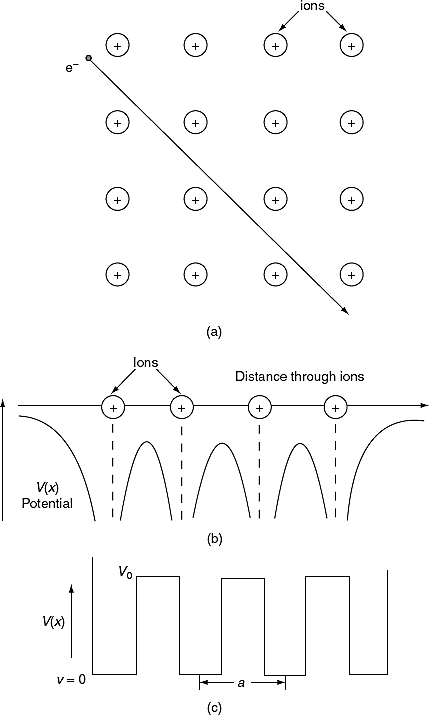
Figure 4
It is not easy to solve Schrödinger’s equation with these potentials. So, Kronig and Penney approximated these potentials inside the crystal to the shape of rectangular steps as shown in Figure 4(c). This model is called Kronig-Penney model of potentials.

Figure 5
The energies of electrons can be known by solving Schrödinger’s wave equation in such a lattice.
The solution to Schrödinger's equation for the Kronig-Penney potential is obtained by assuming that the solution is a Bloch function, namely a traveling wave solution of the form, eikx, multiplied with a periodic solution, u(x), which has the same periodicity as the periodic potential . The total wave function is therefore of the form:

Where u(x) is the periodic function as defined by u(x) = u(x + a), and k(x) is the wave number. We now rewrite Schrödinger equation using this wave function considering first region I, between the barriers where V(x) = 0 and then region II, the barrier region where V(x) = V0:
In region I, Schrödinger's equation becomes:
 (1)
(1)
With
 | (2) |
While in region II, it becomes: |
 | (3) |
With |
 | (4) |
The solution to equations (1) and (4) are of the form : |
 | (5) |
 | (6) |
Since the potential, V(x), is finite everywhere, the solutions for uI(x) and uII(x) must be continuous as well as their first derivatives. Continuity at x = 0 results in:
 | (7) |
And continuity at x = a-b combined with the requirement that u(x) be periodic:
 | (8) |
Results in: |
 | (9) |
Continuity of the first derivative at x = 0 requires that: |
 | (10) |
The first derivatives of uI(x) and uII(x) are: |
 | (11) |
 | (12) |
So that (10) becomes: |
 | (13) |
Finally, continuity of the first derivative at x = a-b, again combined with the requirement that u(x) is periodic, results in:
 | (14) |
So that |
 (15)
(15)
This equation can be simplified using equation (9) to: |
 | (16) |
As a result we have four homogenous equations, (7), (9), (13), and (16), with four unknowns, A, B, C, and D, for which there will be a solution if the determinant of this set of equations is zero, or:
 | (17) |
The first row of the determinant represents equation (7), the second row is obtained by combining (13) and (7), the third row represents equation (9) and the fourth row represents equation (16). This determinant can be rewritten as two determinants, each with three rows and columns, while replacing cosb(a-b) by bc, sinb(a-b) by bs, coshab eika by ac and sinhab eika by as, which results in:
 (18)
(18)
Working out the determinants and using bc2 + bs2 = 1, and ac2 - as2 = e2ika, one finds: |
 | (19) |
And finally, substituting bc, bs, ac and as: |
 | (20) |
Where eika + e-ika was replaced by 2coska. Since the result is independent of the sign of k, this equation also covers all solutions obtained when replacing e-ik by eik in equations (5) and (6).
A further simplification is obtained as the barrier width, b, is reduced to zero while the barrier height, V0, is increased to infinity in such manner that the product, bV0, remains constant and the potential becomes a delta function train at x = a and repeated with a period of a, namely bV0 (x - b - na) where n is an integer. As b approaches zero, sinh b approaches b. Equation (20) then reduces to:
 | (21) |
With |
 | (22) |
The right hand side of equation (21) shows the relation between the energy (through  ) and the wave-vector, k, and as you can see, since the left hand side of the equation can only range from −1 to 1 then there are some limits on the values that
  (and thus, the energy) can take, that is, at some ranges of values of the energy, there is no solution according to these equation, and thus, the system will not have those energies: energy gaps. These are the so-called band-gaps, which can be shown to exist in any shape of periodic potential (not just delta or square barriers). This has been plotted in Figure.
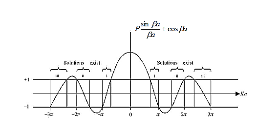
Figure 6: Graph of the right hand side of equation (21) of P for P =2
- The permissible limit of the term

Lies between +1 to -1. By varying  a, a wave mechanical nature could be plotted as shown in Figure, the shaded portion of the wave shows the bands of allowed energy with the forbidden region as unshaded portion.
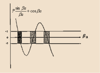
Figure 7
2. With increase of  a , the allowed energy states for a electron increases there by increasing the band width of the bands, i.e., the strength of the potential barrier diminishes. This also leads to increase of the distance between electrons and the total energy possessed by the individual electron.
3.Conversly if suppose the effect of potential barrier dominate i.e., if P is large, the resultant wave obtained in terms of shows a stepper variation in the region lies between +1 to -1. This results in the decrease of allowed energy and increase of forbidden energy gap. Thus at extremities.
Case (i) when P , the allowed energy states are compressed to a line spectrum.
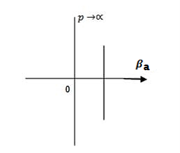
Figure 8
Case (ii) when P the energy band is broadened and it is quasi continuous
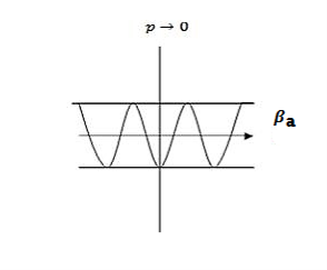
Figure 9
The electron energy forms quasi-continuous bands (because k itself is quasi-continuous) separated from each other by a minimum gap that occurs at ka= s(s = 0, ±1, ±2, ), or k= s/a, at which the left-hand side of Equation (21) is ±1. Figure 10 (b) implies that there are multiple values of k for each E. However, the Bloch theorem says that wave functions corresponding to the wave vectors k separated by m(2/a) (since b= 0) are identical, they are the same quantum state and should be counted only once. Thus, rather than plotting the energy eigenvalues for all the wave vectors, we can plot them in one period, as shown in Figure 11. This way of representation is called the reduced-zone representation. The relationship between the energy and the wave vector is the dispersion relation.
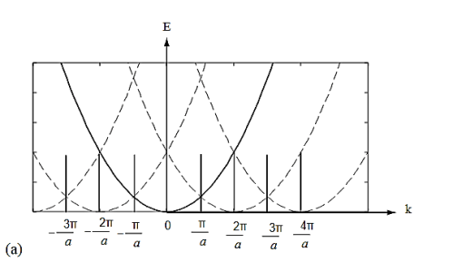
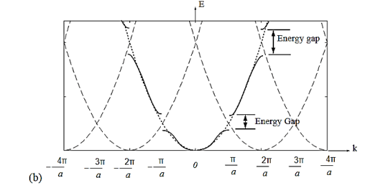
Figure 10
Figure 10 (a) Parabolic energy curves of a free electron in one dimension, periodically continued in reciprocal space. The periodicity in real space is a, and (b) extended zone: splitting of the energy parabola at the boundaries of the first Brillouin zone. The energy gaps are forbidden regions. The solid lines from Kronig-Penney model.
From the E-K diagram is clear that the electron has allowed energy values in the region or zone extending from k= -π/a to k= +π/a. This zone is called first Brillouin Zone. Higher zones can be defined accordingly from the graph.
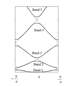
Figure 11: The solid lines show the energy bands in the reduced zone. The free electron dispersion relations are shown as dashed lines.
Consider an isolated silicon atom; its energy levels are quantized. When two identical atoms are brought closer together, the quantized energy levels hybridize and split into two different levels because of the mutual interaction of the two atoms. More generally, when N atoms are moved closer, until they reach the equilibrium inter-atomic distance d, the energy levels split into N levels. These N levels are very close to each other if N is large (which is the case in a crystal) so that they eventually form a continuous energy band.
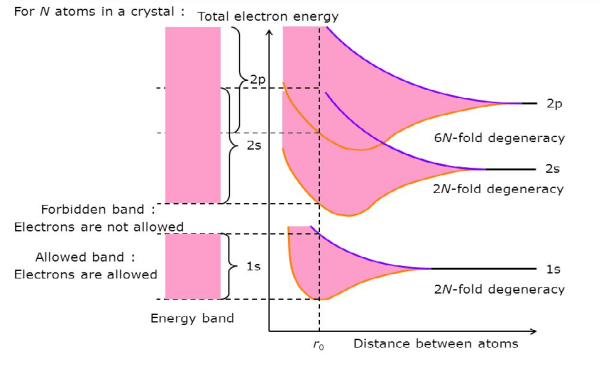
Figure 12: Formation of Energy band as a function of interatomic distance (distance between atoms)
E-K DIAGRAM
The corresponding band structure is shown below (black curve) as well as the energy for a free electron (gray curve). Three different forms are presented, namely the E(k) diagram, the E(k diagram combined with the reduced-zone diagram as well as the reduced-zone diagram only.
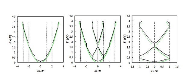
Figure 13: Energy versus ka/π as presented in Figure (black curves) compared to that of a free electron (gray curves). Shown are: a) the E(k) diagram, b) the E(k) diagram combined with the reduced-zone diagram and c) the reduced-zone diagram only.
From Figure 13 a we observe the following: The E(k) relation resembles a parabola except that only specific ranges of energies are valid solutions to Schrödinger's equation and therefore are allowed, while others are not. The range of energies for which there is no solution is referred to as an energy band gap. The transitions between allowed and forbidden energies occur at non-zero integer multiples of ka/ π. These correspond to local minima and maxima of the E(k) relation. The reduced-zone diagram shown in Figure 13 contains the first three bands and energy band gaps. For instance the second energy bandgap occurs between 1.5 and 2 eV, between the band maximum of the second band and the band minimum of the third band.
There may be two separate bands: a conduction band for electrons and a valence band for holes as shown in Figure 14 (a). In many semiconductors such as Si and PbTe, there may be also multiple bands that have the same energy levels, whereby it is called degeneracy. The heavy and light holes are degenerate and the split-off hole in the valence band is slightly off the valence band edge (maximum).
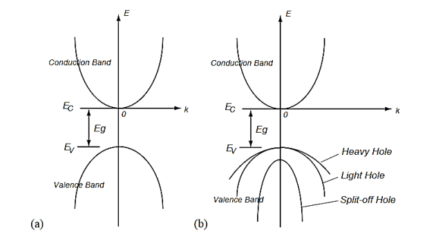
Figure 14 Band structures of a semiconductor including the conduction band and the valence bands.(a) A model of a conduction band and a valence band, and (b) a model of multiple bands.
The type of band gap in semiconductors is important for the selection of material for many electronic devices including thermoelectric devices, solar cells and lasers. There are two types of band gaps in semiconductors, which are direct and indirect band gap. The energy E of a particle is always associated with a wavevector k (or momentum), which implies that, for any transition between bands, both energy and momentum must be conserved. When an electron absorbs enough energy to exceed the energy gap Eg, the electron can jump from the valence band into the conduction band. The source of the energy could be photons, phonons, or electric field.
In direct band gap semiconductors, such as GaAs, the maximum and minimum of energy versus momentum relationship occur at the same value of the wavevector (Figure 15)
In indirect band gap semiconductors like Si and Ge, the maximum and minimum of the energy versus momentum relationship occurs at different wavevectors, which is pictured in Figure 15(b). In this case, the electron cannot directly jump into the conduction band, but once the electron at the valence band edge EV absorbs energy (photon, phonon, or electric field) and reaches the energy level of the conduction band edge EC across the energy band Eg, it can indirectly jump into the conduction band with the aid of phonon energy because phonon usually exists anyway.
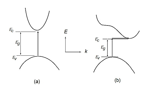
Figure 15: Energy versus wavevector diagrams in (a) direct band gap and (b) indirect band gap semiconductors
Direct and indirect gap semiconductors have major differences in their optical properties. Direct band gap semiconductors are more efficient photon emitters, semiconductor lasers are made of direct gap semiconductors such as GaAs, whereas most electronic devices including thermoelectric devices are built on indirect semiconductors.
The band gap represents the minimum energy difference between the top of the valence band and the bottom of the conduction band, however, the top of the valence band and the bottom of the conduction band are not generally at the same value of the electron momentum. In a direct band gap semiconductor, the top of the valence band and the bottom of the conduction band occur at the same value of momentum, as in the schematic below.
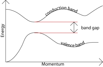
Figure 16:
In an indirect band gap semiconductor, the maximum energy of the valence band occurs at a different value of momentum to the minimum in the conduction band energy:
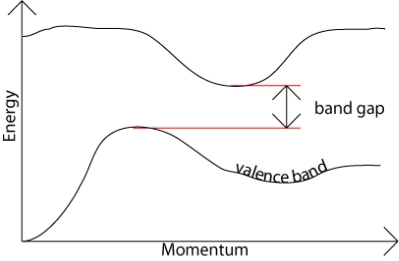
Figure 17
Photon can provide the energy to produce an electron-hole pair. Each photon of energy E has momentum p = E / c, where c is the velocity of light. An optical photon has energy of the order of 10–19 J, and, since c = 3 × 10⁸ ms–1, a typical photon has a very small amount of momentum.
A photon of energy Eg, where Eg is the band gap energy, can produce an electron-hole pair in a direct band gap semiconductor quite easily, because the electron does not need to be given very much momentum. However, an electron must also undergo a significant change in its momentum for a photon of energy Eg to produce an electron-hole pair in an indirect band gap semiconductor. This is possible, but it requires such an electron to interact not only with the photon to gain energy, but also with a lattice vibration called a phonon in order to either gain or lose momentum.
The indirect process proceeds at a much slower rate, as it requires three entities to intersect in order to proceed: an electron, a photon and a phonon. This is analogous to chemical reactions, where, in a particular reaction step, a reaction between two molecules will proceed at a much greater rate than a process which involves three molecules.
The same principle applies to recombination of electrons and holes to produce photons. The recombination process is much more efficient for a direct band gap semiconductor than for an indirect band gap semiconductor, where the process must be mediated by a phonon.
As a result of such considerations, gallium arsenide and other direct band gap semiconductors are used to make optical devices such as LEDs and semiconductor lasers, whereas silicon, which is an indirect band gap semiconductor, is not. The table in the next section lists a number of different semiconducting compounds and their band gaps, and it also specifies whether their band gaps are direct or indirect.
Table :I
| Material | Direct / Indirect Bandgap | Band Gap Energy at 300 K (eV) |
|
|
|
|
Groups III-V compounds | GaAs | Direct | 1.42 |
Groups IV-IV compounds | α-SiC | Indirect | 2.99 |
Groups II-VI compounds | ZnO | Direct | 3.35 |
AND INSULATORS,
Modern electronics, which has revolutionized our way of life, is based on interesting properties of a class of material. The free electron model of metals gives us good insight into the electrical conductivity and electrodynamics of metals. But the model fails to help us with other questions, for example the relation of conduction electrons in the metal to the valence electrons of free atoms and many transport properties. Every solid contains electrons. The important question for electrical conductivity is how electrons respond to an applied electric field. We shall see that electrons in crystals are arranged in energy bands separated by regions in energy for which no wavelike electron orbits exist. Such forbidden regions are called energy gaps or band gaps(𝐸𝐺), wherein the differences between a metal, a semiconductor and an insulator are summarized schematically .The crystal behaves as an insulator if the allowed energy bands are all either filled or empty, for then no electrons can move in an electric field. The crystal behaves as a metal if one or more bands are partly filled. The crystal is a semiconductor or semimetal if one or two bands are slightly filled or slightly empty.
To understand the difference between insulators and conductors, we must extend the free electron model to take account of the periodic lattice of the solid.
Once we know the band structure of a given material we still need to find out which energy levels are occupied and whether specific bands are empty, partially filled or completely filled.
Empty bands do not contain electrons. Therefore, they are not expected to contribute to the electrical conductivity of the material. Partially filled bands do contain electrons as well as available energy levels at slightly higher energies. These unoccupied energy levels enable carriers to gain energy when moving in an applied electric field. Electrons in a partially filled band therefore do contribute to the electrical conductivity of the material.
Completely filled bands do contain plenty of electrons but do not contribute to the conductivity of the material. This is because the electrons cannot gain energy since all energy levels are already filled.
In order to find the filled and empty bands we must find out how many electrons can be placed in each band and how many electrons are available. Each band is formed due to the splitting of one or more atomic energy levels. Therefore, the minimum number of states in a band equals twice the number of atoms in the material. The reason for the factor of two is that every energy level can contain two electrons with opposite spin.
To further simplify the analysis, we assume that only the valence electrons (the electrons in the outer shell) are of interest. The core electrons are tightly bound to the atom and are not allowed to freely move in the material.
Four different possible scenarios are shown in Figure 18
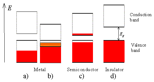
Figure 18
A half-filled band is shown in Figure 18
a). This situation occurs in materials consisting of atoms, which contain only one valence electron per atom. Most highly conducting metals including copper, gold and silver satisfy this condition. Materials consisting of atoms that contain two valence electrons can still be highly conducting if the resulting filled band overlaps with an empty band. This scenario is shown in
b). No conduction is expected for scenario
d) where a completely filled band is separated from the next higher empty band by a larger energy gap. Such materials behave as insulators.
Finally, scenario c) depicts the situation in a semiconductor. The completely filled band is now close enough to the next higher empty band that electrons can make it into the next higher band. This yields an almost full band below an almost empty band. We will call the almost full band the valence band since it is occupied by valence electrons. The almost empty band will be called the conduction band, as electrons are free to move in this band and contribute to the conduction of the material.

Figure 19
- In Conductors: The valance band and the conduction band overlap each other. This makes it easy for the electricity to pass through them. In conductors, the valence band is either not fully occupied with electrons, or the filled valence band overlaps with the empty conduction band. In general, both states occur at the same time, the electrons can therefore move inside the partially filled valence band or inside the two overlapping bands. In conductors there is no band gap between the valence band and conduction band.
- In Semi-conductors: there is a slight gap between the conduction band and the valance band. This band gap is less than or equal to 1.4 eV. The electrons from valance shell take a little energy to excite from valance band to the conduction band. Even in semiconductors, there is a band gap, but compared to insulators it is so small that even at room temperature electrons from the valence band can be lifted into the conduction band. The electrons can move freely and act as charge carriers.
- In Insulators: In insulators the valence band is fully occupied with electrons due to the covalent bonds. To achieve conductivity, electrons from the valence band have to move into the conduction band. the energy gap is considerably large and the electrons of the valance band cannot be excited to the conduction band before the melting or the dissociation of the solid. This means that under the practically ambient condition it cannot conduct electricity.
Density of Energy States
The Fermi function gives the probability of occupying an available energy state, but this must be factored by the number of available energy states to determine how many electrons would reach the conduction band. This density of states is the electron density of states, but there are differences in its implications for conductors and semiconductors. For the conductor, the density of states can be considered to start at the bottom of the valence band and fill up to the Fermi level, but since the conduction band and valence band overlap, the Fermi level is in the conduction band so there are plenty of electrons available for conduction. In the case of the semiconductor, the density of states is of the same form, but the density of states for conduction electrons begins at the top of the gap.
Fermi function F (E):
Fermi-Dirac distribution function represents the probability of an electron occupying a given energy level at absolute temperature. It is given by

Where KB Boltzmann Constant
T Temperature
If g(E) is the density of states and f(E) gives the probability of occupation of those states at a given temperature, the number of occupied states, n(E),is given by
n(E) =  (1)
(1)
If the number of occupied states in an energy band needs to be calculated the integration needs to be performed over the entire band. This will be a function of temperature, since the Fermi function is temperature dependent. Equation 1 can be used to calculate the concentration of electron and holes in semiconductors, which decides their conductivity.
Effect of temperature on Fermi Function:
Case (i) Probability of occupation for E < EF at T = 0K

When T = 0K and E < EF, we have
F(E) =  =
=  = 1
= 1
Thus at T = 0K, there is 100 % chance for the electrons to occupy the energy levels below the Fermi level.
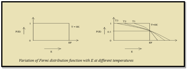
Figure 20: Fermi distribution
Case (ii) Probability of occupation for E>EF at T = 0K
When T = 0K and E > EF, we have
F(E) =  =
=  =
=  = 0
= 0
Thus, there is 0 % chance for the electrons to occupy energy levels above the Fermi energy level. From the above two cases, at T = 0K the variation of F(E) for different energy values becomes a step function.
Case (iii) Probability of occupation at ordinary temperature
At ordinary temperature, the value of probability starts reducing from 1 for values of E slightly less than EF. With the increase of temperature, i.e., T> 0K, Fermi function F (E) varies with E.
At any temperature other than 0K and E = EF
F(E) =  =
=  =
=  = 50%
= 50%
Hence, there is 50 % chance for the electrons to occupy Fermi level. Further, for E > EF the probability value falls off rapidly to zero.
Case (iv) At high temperature
When kT >> EF, the electrons lose their quantum mechanical character and Fermi distribution function reduces to classical Boltzmann distribution
Fermi level" is the term used to describe the top of the collection of electron energy levels at absolute zero temperature. This concept comes from Fermi-Dirac statistics. Electrons are fermions and by the Pauli exclusion principle cannot exist in identical energy states. So at absolute zero they pack into the lowest available energy states and build up a "Fermi sea" of electron energy states. The Fermi level is the surface of that sea at absolute zero where no electrons will have enough energy to rise above the surface.
The concept of the Fermi energy is a crucially important concept for the understanding of the electrical and thermal properties of solids. Both ordinary electrical and thermal processes involve energies of a small fraction of an electron volt. But the Fermi energies of metals are on the order of electron volts. This implies that the vast majority of the electrons cannot receive energy from those processes because there are no available energy states for them to go to within a fraction of an electron volt of their present energy. Limited to a tiny depth of energy, these interactions are limited to "ripples on the Fermi sea".
At higher temperatures a certain fraction, characterized by the Fermi function, will exist above the Fermi level. The Fermi level plays an important role in the band theory of solids. In doped semiconductors, p-type and n-type, the Fermi level is shifted by the impurities, illustrated by their band gaps. The Fermi level is referred to as the electron chemical potential in other contexts.
In metals, the Fermi energy gives us information about the velocities of the electrons which participate in ordinary electrical conduction. The amount of energy which can be given to an electron in such conduction processes is on the order of micro-electron volts (see copper wire example), so only those electrons very close to the Fermi energy can participate. The Fermi velocity of these conduction electrons can be calculated from the Fermi energy.
This speed is a part of the microscopic Ohm's Law for electrical conduction. For a metal, the density of conduction electrons can be implied from the Fermi energy. | 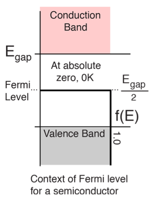 Figure 20
|
The Fermi energy also plays an important role in understanding the mystery of why electrons do not contribute significantly to the specific heat of solids at ordinary temperatures, while they are dominant contributors to thermal conductivity and electrical conductivity. Since only a tiny fraction of the electrons in a metal are within the thermal energy kT of the Fermi energy, they are "frozen out" of the heat capacity by the Pauli principle. At very low temperatures, the electron specific heat becomes significant.
It is named after the Physicist Enrico Fermi. A Fermi level is the measure of the energy of least tightly held electrons within a solid. It is important in determining the thermal and electrical properties of solids. It can be defined as:
The Fermi energy is a concept in quantum mechanics usually refers to the energy difference between the highest and lowest occupied single-particle states in a quantum system of non-interacting fermions at absolute zero temperature.
The value of the Fermi level at absolute zero temperature is known as the Fermi energy. It is also the maximum kinetic energy an electron can attain at 0K. Fermi energy is constant for each solid.
To determine the lowest possible Fermi energy of a system, we first group the states with equal energy into sets and arrange them in increasing order of energy. We then add particles one at a time, successively filling up the unoccupied quantum states with the lowest energy.
When all the particles are arranged accordingly, the energy of the highest occupied state is the Fermi energy.
In Spite of the extraction of all possible energy from metal by cooling it to near absolute zero temperature (0 Kelvin), the electrons in the metal still move around. The fastest ones move at a velocity corresponding to a kinetic energy equal to the Fermi energy.
The highest energy level that an electron can occupy at the absolute zero temperature is known as the Fermi Level. The Fermi level lies between the valence band and conduction band because at absolute zero temperature the electrons are all in the lowest energy state. Due to lack of sufficient energy at 0 Kelvin, the Fermi level can be considered as the sea of fermions (or electrons) above which no electrons exist. The Fermi level changes as the solids are warmed and as electrons are added to or withdrawn from the solid.
Don’t get confuse between Fermi level and Fermi energy. Both the terms are equal at absolute zero temperature but they are different at other temperature.
In reality, an electron in a crystal experiences complex forces from the ionized atoms. We imagine that the atoms in the linear chain form the electrical periodic potential. If the free electron mass m is replaced by the effective mass m*, we can treat the motion of electrons in the conduction band as free electrons. An exact defined value of the wavevector k, however, implies complete uncertainty about the electron’s position in real space. Mathematically, localization can be described by expressing the state of the electron as a wave packet, in other words, a group velocity. The group velocity of electrons in Figure 21 is the slope of the dispersion relation.
vg  (1)
(1)
Since the wavelength is twice the lattice constant a, the boundaries at the zone in k-space is k= ± /a. The frequency associated with a wave vector of energy E is
E ℏ and p ℏk (2)
Where the two equations are known as the Planck-Einstein relations.
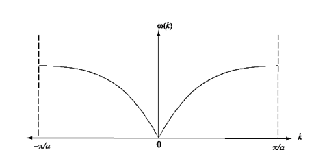
Figure 21: Dispersion relation of a group of electrons with a nearest neighbour interaction. Note that is linear for small k, and that  vanishes at the boundaries of the Brillouin zone (k= ± /a)
vg  (3)
(3)
The derivative of Equation (3) with respect to time
 =
=  =
=  (4)
(4)
From Equation (2), we have mvgℏk and m The force acting on the group of electrons is then
F = m (5)
(5)
Combining Equations (4) and (5) yields
F =  (6)
(6)
This indicates that there is an effective mass m*, which will replace the electron mass m.
 (7)
(7)
The effective mass m*is the second order of derivative of energy with respect to wavevector, which is representative of the local curvature of the dispersion relation in three dimensional space. The effective mass is a tensor and maybe obtained experimentally or numerically.
A phonon is a quantized mode of vibration occurring in a rigid crystal lattice, such as the atomic lattice of a solid. The study of phonons is an important part of solid state physics, because phonons play an important role in many of the physical properties of solids, such as the thermal conductivity and the electrical conductivity. In particular, the properties of long-wavelength phonons give rise to sound in solids -- hence the name phonon. In insulating solids, phonons are also the primary mechanism by which heat conduction takes place.
Phonons are a quantum mechanical version of a special type of vibrational motion, known as normal modes in classical mechanics, in which each part of a lattice oscillates with the same frequency. These normal modes are important because, according to a well-known result in classical mechanics, any arbitrary vibrational motion of a lattice can be considered as a superposition of normal modes with various frequencies; in this sense, the normal modes are the elementary vibrations of the lattice. Although normal modes are wave-like phenomena in classical mechanics, they acquire certain particle-like properties when the lattice is analysed using quantum mechanics. They are then known as phonons. Phonons are bosons possessing zero spin.
A phonon is the elementary excitation in the quantum mechanical treatment of vibrations in a crystal lattice or the quantum unit of a crystal lattice vibration.
They are analogous to photons, having energy of ћω as quanta of excitation of the lattice vibration mode of angular frequency ω. Since the momentum ћk is exact, by the uncertainty principle, the position of phonons cannot be determined, and so, phonons are not localized particles. Nevertheless, just like the case with photons or electrons, a fairly localized wavepacket can be constructed by combining modes of slightly different frequency and wavelength. By taking waves with a spread of k of order π/10a, a wavepacket localized within about 10 unit cells are made, representing a fairly localized phonon with group velocity dω/dk; within the limits of the uncertainty principle.
Although it is convenient to interpret ћk as the phonon momentum, it is not really the true kinematic momentum and often referred to as ‘crystal momentum’. In a 1D crystal lattice, a lattice mode with wavenumber k can be equally represented by a wavenumber k + 2πn/a. Therefore, it is not possible to give a unique value of k to a phonon.
Like photons, phonons are bosons and not conserved; they can be created or destroyed in collisions. Phonons, through emission or absorption, scatter inelastically with neutrons by experiment and determines the phonon dispersion relations ω(k). The ω(k) curve for lattice vibrations can be interpreted with both axes multiplied by ћ, as a relation between energy and momentum for phonons ( E = ћω, p = ћk ). Phonon dispersion relation shows features in crystals with two or more atoms per primitive basis.
If a phonon with wavevector  is created by inelastic scattering of a photon or neutron from wavevector
  to
to  , the wavevector selection rule that governs the process is

Where  is a reciprocal lattice vector
ACOUSTIC PHONONS AND OPTICAL PHONONS
When the unit cell contains more than one atom, the crystal will contain two types of phonon, acoustic and optical. Optical phonons are excited easily by light. In acoustic phonons, both positive and negative ions swing together. In optical phonons, positive and negative phonons swing against each other.
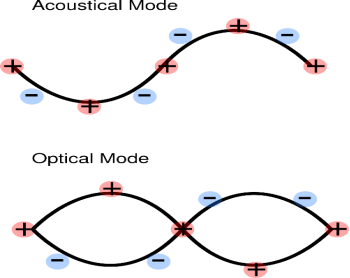
Figure 22
Phonon Energy
If the angular frequency of a phonon is given by ω, then the energy of the phonon is 
Phonon-phonon collision

Figure 23: A collision where phonon 1 and 2 coalesce to give phonon 3.
In figure 23, a phonon of wavenumber k1 and frequency ω1 coalesces with a phonon of wavenumber k2 and frequency ω2 to produce phonon 3 with wavenumber k3 and frequency ω3.
