Module 2
Semiconductors
Definition: When a semiconductor is in Thermal equilibrium, the supply function of the electrons at the energy level of E is presented by a Fermi –Dirac delivery function.
In this case the Fermi level is defined as the level in which the probability of work of electron at that energy is ½.
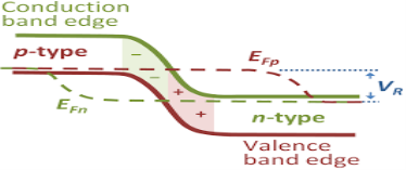
In thermal equipoise, there is no need to distinguish between conduction band quasi-Fermi level and valence band quasi-Fermi level as they are simply equivalent to the Fermi level.
The electron in conduction band which is in equilibrium is given by
ne = Neffe · exp – | EC – EF kT |
The holes in valance band which is in symmetry is given by
nh = Neffh · exp – | EF – EV kT |
Balance means -holes and electron are equal in band this resources fermi energy is same or equal for both bands

Now for the equation of Fermi we must write down f(E, EFe, T) or f(E, EFh, T) instead of f(E,Ef,T) or E f
.
The carrier concentration of electron or holes in conduction or valance band are as follow
ne = Neffe · [fe in C(E, EFe, T)]Neffe · exp - 
The carrier concentration of electron or holes in conduction or valance band are as follow
ne = Neffn · [fn in C(E, EFn, T)]Neffn · exp - 
This can be cured easily by simply setting 1 – f(E, EFh, T) =: fh in V(E, EFh, T) with fh in V existence the probability of finding holes on the available states in the valence band.
Formally, the electron density in the valence band (EV) then contains 1 – fh in V and so on.
Any disturbance of free carriers in a semiconductor form a current( I). This disturbance can be formed by an electric field due to an externally applied voltage(V), since the carriers are charged particles.
- This is transfer as carrier drift. In addition, carriers also move from areas high to low carriers.
- This carrier transport mechanism is reason by the thermal energy and the associated random motion of the carriers.
- We will consider this carriage mechanism as carrier diffusion.
- The overall current in a semiconductor generations the addition of the drift and the diffusion current.
- After pass electric field to a semiconductor, the electrostatic force causes the carriers to first accelerate and then grasp a constant average velocity, v, due to collisions with impurities and lattice vibrations.
- Mobility is known as the ratio of the velocity to the practical field .
- Diffusion of carriers is obtained by making a carrier density gradient.
- Such gradient can be obtained by changing the doping density in a semiconductor or by applying a thermal gradient.
- Both carrier transport mechanisms are connected since the same particles and scattering mechanisms are involved.
- This leads to association between the mobility and the diffusion constant called the Einstein relation.

Definition: A p-n junction is an interface or a boundary between two semiconductor material types, namely the p-type and the n-type, inside a semiconductor.
p type semiconductor have hole as majority carrier while minority carrier electron
similarly n type have majority electron and minority carrier hole
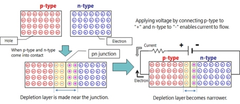
When p-type and n-type come into contact depletion layer is made near the junction.
Connecting battery positive terminal at p type and n type then we can get narrower depletion layer this kind of bias is known as forward bias while after changing terminal we can get reverse bias.
Flow of electron and current are opposite to each other.
Metal-Semiconductor Junction (Ohmic And Schottky):
Whenever a metal and a semiconductor come together, there emerging of a potential barrier between the two that prevents most charge electrons or holes from passing from one to the other.
Small number of carriers has the energy to get over out of material.
When a bias is applied to the junction either it can make the barrier seem lower from the semiconductor side, or it can make it appear higher.
The bias neither changes the barrier height from the metal side.
Finally, this is a Schottky Barrier (rectifying contact), where the junction conducts for one bias polarity, but not the other.
About all metal-semiconductor junctions exhibit some of this rectifying performance.
Schottky Contacts make good diodes and may even be used to make a sympathetic of transistor, but for getting signals into and out of a semiconductor device, we are interested in Ohmic contacts.
Ohmic contacts conduct the same for both polarities (negative and positive). (They follow Ohm's Law).
There are two ways to make a metal-semiconductor contact look ohmic enough to get signals into and out of a semiconductor (or doing the opposite makes a good Schottky contact).
Lower the barrier height
We will use those materials whose barrier height is minor.
Strengthening may form an alloy between the semiconductor and the metal at the junction, which can also inferior the barrier height.
Make the barrier very narrow
One very interesting property of very tiny particles like electrons and holes is that they can "tunnel" through barriers that they don't have sufficient energy to just pass over.
The probability of tunnelling becomes high for very thin barriers .
We make the barrier actual thinnest by doping it very heavily (1019 dopant atoms/cm3 or more).
References:
1.J.Singh, Semiconductor Optoelectronics: Physics and Technology, McGraw-HillInc.(1995).
2.B.E.A .Saleh and M. C.Teich, Fundamentals of Photonics, John Wiley &Sons, Inc.,(2007).
3.S.M.Sze, Semiconductor Devices: Physicsand Technology, Wiley(2008).
4.A.Yariv and P.Yeh, Photonics: Optical Electronic sin Modern Communications ,Oxford University Press, New York(2007).
5.P.Bhattacharya, Semiconductor Optoelectronic Devices ,Prentice Hall of India(1997).
6. Engineering Physics by Dattu R Joshi, McGraw hill Publications.