Unit V
Nano material
Content
The designing and making up of anything whose use depends on the specific structure at nanoscale. These posses the different properties at reducing scale. The measurement can be taken in notice at 100 nanometers and lesser is called as the nanotechnology. This includes the materials made by the manipulation of up of atoms or molecules. They are composed up of metals, ceramics, polymers, organic materials in simpler way these all are made up of carbon compounds. The technology that we deal with in taking the consideration up of the Nano material is called as the nanotechnology.
Some nano materials occur naturally, but of particular interest are engineered nanomaterials (EN), which are designed for, and already being used in many commercial products and processes. They can be found in such things as sunscreens, cosmetics, sporting goods, stain-resistant clothing, tires, electronics, as well as many other everyday items, and are used in medicine for purposes of diagnosis, imaging and drug delivery. Nano materials are found basically form following three sources:
1) Engineered
2) Incidental
3) Natural
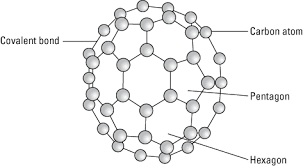
It is an allotropic form of the carbon atom (Allotropy form- When any element is formed in more than one form and in each form they posses different property). An Er. & Scientist Richard Buckminster Fuller extracted that carbon is having cluster the very first form gathered is C16.
Structure:
Fullerene is a soccer ball like structure which is hollow from inside and is polymorphic in nature (arrange in hexagon and pentagon form) These are arranged in manner that posses 2 hexagon share a common wall while 2 different pentagon never share the common wall. Each carbon atom is sp2 hybridized. Electric spark is produced at graphite ectrode at inert atmosphere and low pressure which gives back black soot that consist of fullerene and impurities. These impurities are removed by the method of sublimation.

Properties:
All carbon atoms are sp2 hybridized with FCC in nature. This is mustard yellow in color. The fullerene may be Exohederal or Endohederal structure based on the occupying the space.
Applications:
1-Used as super conductors
2-Fulleren is used in making the Ferro magnets
3-It can be used for making non-linear electronic devices.
Nano materials are used in optoelectronics due to their interesting optical and electrical properties. Furthermore, the optical and electronic properties of nano materials which depend on their size and shape can be tuned via synthetic techniques. Nano particles are used in optoelectronic devices such as OLEDs etc. The operating principles of such devices depend on photo induced processes like electron transfer and energy transfer. The performance of the devices depends on the efficiency of the photo induced process responsible for their functioning. Therefore, better understanding of those photo induced processes in organic and inorganic nano material composite systems is necessary in order to use them in optoelectronic devices.
Nano particles made of metals, semiconductors or oxides are of particular interest for their mechanical, electrical, magnetic, optical, chemical and other properties. Nano particles have been used as quantum dots and as chemical catalysts such as nano material based catalysts.
Nano particles act as a bridge between bulk materials and molecular structures. A bulk material should have constant physical properties regardless of its size, but at the nano-scale this is often not the case. Size-dependent properties are observed such as quantum confinement in semiconductor particles, surface plasmon resonance in some metal particles and super para magnetism in magnetic materials.
Nano particles exhibit a number of special properties relative to bulk material. E.g.: the bending of bulk copper occurs with movement of copper atoms.
Nano tubes: Carbon nano tubes (CNTs) are cylindrical molecules that consist of rolled-up sheets of single-layer carbon atoms. They can be single-walled with a diameter of less than 1 nm or multi-walled, consisting of several concentrically interlinked nano tubes, with diameters reaching more than 100 nm. Their length can reach several micrometers or even millimeters.
Like their building block graphene, CNTs are chemically bonded with sp2 bonds, an extremely strong form of molecular interaction. This feature combined with carbon nano tubes natural inclination to rope together via van der Waals forces, provide the opportunity to develop ultra-high strength, low-weight materials that possess highly conductive electrical and thermal properties. This makes them highly attractive for numerous applications.
The rolling-up direction of the graphene layers determines the electrical properties of the nano tubes. Chirality describes the angle of the nano tube's hexagonal carbon-atom lattice.
Armchair nano tubes – so called because of the armchair-like shape of their edges – have identical chiral indices and are highly desired for their perfect conductivity. They are unlike zigzag nano tubes, which may be semiconductors. Turning a graphene sheet a mere 30 degrees will change the nano tube it forms from armchair to zigzag or vice versa.
While MWCNTs are always conducting and achieve at least the same level of conductivity as metals, SWCNTs' conductivity depends on their chiral vector: they can behave like a metal and be electrically conducting; display the properties of a semi-conductor; or be non-conducting. For example, a slight change in the pitch of the helicity can transform the tube from a metal into a large-gap semiconductor.
Nano wires: Nanowires are cylindrical solid wires structures with one of the dimensions smaller than 100 nm and length few micrometers. Nanowires are quantum mechanically one dimensional structures when their diameter is comparable to the electron’s de Broglie wavelength in the plane perpendicular to the growth direction. One dimensional confinement of electrons in nano wires causes the change in density of states and allowed energy levels in nano wires. Quantum confinement in nano wires also allows the study of other unique phenomena such as ballistic transport, coulomb blockade and phonon confinement. One interesting phenomena observed in nano wires is that the band gap is altered according to requirement which is an important parameter in fabricating devices for specific applications. Since the band gap increases with the decrease of nano wire diameter, nano wire can emit visible light with high efficiency. Nano wire band gap is also affected by the surface chemistry because of the high surface area to volume ratio. Depending on the passivant on the nano wire surface the band gap can also be increased or decreased accordingly. A well accepted mechanism for the growth of nano wires through gas phase reaction is vapour liquid-solid process. To grow any nano wire, the material used must be soluble in the catalyst nano particles. E.g.: to grow silicon nano wire gold nano particles are used because silicon vapour is soluble in gold nano particles. To grow gallium nitride nano wire iron nano particles are used because the reactants gallium and nitrogen are soluble in iron nano particles.
Top Down Approach
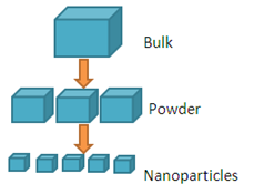
Top down approach deals with the breaking down of bulk material into nano sized particles. Top-down synthesis techniques are extension of those that have been used for producing micron sized particles. Top-down approaches are inherently simpler and depend either on removal or division of bulk material or on miniaturization of bulk fabrication processes to produce the desired structure with appropriate properties. The biggest problem with the top-down approach is the imperfection of surface structure. E.g.: nano wires made by lithography are not smooth and may contain a lot of impurities and structural defects on its surface.

Bottom Up Approach
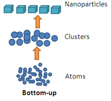
Bottom –up approach refers to the build-up of a material from the bottom: atom-by-atom, molecule-by-molecule or cluster-by-cluster. This route is more often used for preparing most of the nano-scale materials with the ability to generate a uniform size, shape and distribution. It effectively covers chemical synthesis and precisely controlled the reaction to inhibit further particle growth. Although the bottom-up approach is nothing new, it plays an important role in the fabrication and processing of nanostructures and nano materials.

Nanoelectronics refers to the use of nanotechnology in electronic components. The term covers a diverse set of devices and materials, with the common characteristic that they are so small that inter-atomic interactions and quantum mechanical properties need to be studied extensively. Some of these candidates include: hybrid molecular/semiconductor electronics, one-dimensional nano tubes.
Nano electronic devices have critical dimensions with a size range between 1 nm and 100 nm. Recent silicon MOSFET (metal-oxide-semiconductor field-effect transistor, or MOS transistor) technology generations are already within this regime, including 22 nanometer CMOS (complementary MOS) nodes and succeeding 14 nm, 10 nm and 7 nm Fin FET (fin field-effect transistor) generations. Nano electronics are sometimes considered as disruptive technology because present candidates are significantly different from traditional transistors.
Applications:
1- Nano material will be used as the next generation computer chips.
2- Nano material will be responsible for the High Definition TV.
3- Branch deals in reducing the cost of the flat panel displays.
4- Nanotechnology plays a major role in improving the density of the battery.
5- Nanotechnology contributes in the changing trends by playing the major role in improving the sensivity of the sensors.
Reference Books:
1. Engineering Chemistry by Jain and Jain, Dhanpat Rai Publishing Co.
2. Engineering Chemistry Willey India Publisher
3. Engineering Chemistry by Marry Jane & Shultz, Cencage Learning Publisher
4. Engineering Chemistry by N. Krishnamurthy, P. Vallinaygam and D. Madhavan,
Prentice Hall of India Pvt. Ltd.
5. Engineering Chemistry by K. Sesha Maheswaramma and Mridula Chugh, Pearson India Education Pvt Ltd.
6. Engineering Chemistry by B K. Sharma, Krishna Prakashan Media (P) Ltd.
7. A textbook of Engineering Chemistry by Shashi Chawla, Dhanpatrai Publishing Co. Ltd.
8. Fundamentals of Biotechnology by B D Singh, Kalyani Publisher. New Delhi.
9. Essential of Physical Chemistry by Bahl and Tuli., S Chand & Co. Ltd, New Delhi.
10. Introduction to Nano Science by N N. Lindsay, Oxford University Press.
11. NANO: The Essentials by T Pradeep Tata McGraw-Hill Publishing Company, New Delhi.