Unit-I
Evaluation of Electronics:
- Electronics vegan with invention of vacuum diode by J.A Fleming in 1897 and after that vacuum triode invented by lee de forest to amplify the signals.
- The Transistor Era began with the junction transistor invention in1948.from 1958 to 1975. Integrated circuits (Ic’s) introduced which is a small signal chip such as small scale & very large scale integration .
- . Integrated circuits drastically changed the entire electronics natures as entire electronic circuit of integrated in a signal chip which has low cost ,small size, light in weight& more reliable.
- . The Use Off Germanium and silicon semiconductor materials made these transistor gain the popularity & widely used in deferent electronics circuits & devise.
Electronics engineering Field Have become an important part of human being. Starting with an electronic alarm to get up early in the morning, watch to update current news , microwave oven is used to cook the food , washing machine is used to clean our clothes 7 for entertainment music system is used. Now a days electronics devices everywhere is utilized such as in schools, colleges , homes, shops, health care, defence ,industries ,research, geographic, animation, etc
- The electronics industry is growing very fast & is creating good job opportunity in industries like mobile phone, IT Industries television, computers, laptops, tablets, & palmtops.
- In Addition to this there are good carrier options in consumer durables, oil, gas chemical &power electronics.
- In has many Applications ranging from healthcare satellite communication, mobile communication (2G,3G,& 4G) & Internet technology.
- Engineers with Bachelor of Electronics & Telecommunication can work in research, design & development & manufacturing of electronics applications.
- They also have job openings in sale & marketing of electronic Equipment& maintaining & repairing of electronic devices.
- It has various fields such as VLSI Design .Microwave Engineering Integrated CKT .embedded system Nanotechnology, microelectronics & artificial intelligence soon.
Applications:-
1) Digital Commerce
Ii) Mobile Phone
Iii) Computers
Iv) Medical applications such as CT scan 1MRI
v) Led traffic lights
Vi) Led displays etc
According to Neil Bohr’s theory of atomic structure all atoms have different energy levels. When two or more atoms are placed near to each other their energy levels get transformed to energy band structure. These energy bands are formed due to mutual interaction between the atoms caused by the electromagnetic force between them.
The below figure shows the energy bands of various energy levels. The electrons nearer to nucleus of interacting atom are having energy band 1 and those in outer orbit have E2, E3 so no.

Fig: Energy band in crystal
Energy band in crystals can of different types which are
i) Valence Band: The electrons in the outer most orbit of an atom is present in this energy band. This is the highest energy band at room temperature. This band can be completely or partially filled.
Ii) Conduction Band: This is the lowest energy band containing electrons which are free from the attractive force of atom’s nucleus.
The Valence band has low energy level than conduction band. This is the reason that CB is above the VB separated by energy gap.
Below shown is the figure of energy band for metals, semiconductors and insulators. The conduction in materials is possible only because of the electrons present in the conduction band.
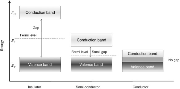
Fig: Energy band for Conductors, Semi-conductors and Insulators
From the above figure the conductors (metals) have both the energy bands overlapping. This shows that they have large number of free electrons which make them the good conductors.
There is one more energy band shown above having a huge gap between CB and VB which significantly shows that we need to provide large amount of energy to the electrons to jump form VB to CB. But this amount of energy is not possible to be applied and hence no movement of electron is seen. There is no conduction possible making them insulator.
The last one seen from above figure has a difference in CB and VB but the energy gap is such that after applying external voltage some of the electrons can jump from VB to CB. These are semi-conductorswhich can be made to conduct as conductors by exciting them externally.
N type Semiconductor:
To increase the number of conduction band electrons intrinsic silicon, pentavalent imparity atoms are added. These are atoms with five valence electrons such as
i) arsenic (as)
Ii) phosphors (p)
Iii) Bismuth (Bi)
Iii) Antimony ( sb)
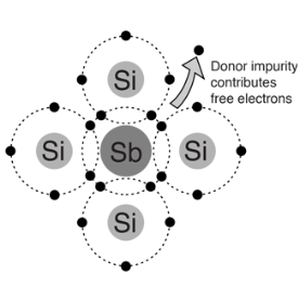
- Pentavalent impurity atom in a silicon crystal. An antimony (sb) impurity atom shown above-
- Each pentavalent atom forms covalent bonds with four adjustment silicon atoms, leaving one extra electron.
- The pentavalentatom gives up on electron, it often called a donor atom.
- Majority and minority carriers:- A type here means negative charge of an electron .electron are called the majority carriers in n-type material.
- Hole in an n-type material are called minority carriers
P Type Semiconductor:-
To increase the number of holes in intrinsic silicon trivalent impurity atoms are added these are atoms with their valence electrons such as
i) Baron(B)
Ii) Indium(IN)
Iii)Gallium(GO)
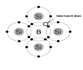
- Trivalent impurity atom in a silicon crystal structure. A) boron (B) impurity atom is shown in the center.
- The number of holes can be carefully controlled by the number of trivalent impurity atoms added to the silicon .
- A Hole created by the doping process is not accompanied by a conduction (free) electron.
- Trivalent Atom can take an electron it is often referred to as on accepted atom
Any disturbance of free carriers in a semiconductor form a current( I). This disturbance can be formed by an electric field due to an externally applied voltage(V), since the carriers are charged particles.
- This is transfer as carrier drift. In addition, carriers also move from areas high to low carriers.
- This carrier transport mechanism is reason by the thermal energy and the associated random motion of the carriers.
- We will consider this carriage mechanism as carrier diffusion.
- The overall current in a semiconductor generations the addition of the drift and the diffusion current.
- After pass electric field to a semiconductor, the electrostatic force causes the carriers to first accelerate and then grasp a constant average velocity, v, due to collisions with impurities and lattice vibrations.
- Mobility is known as the ratio of the velocity to the practical field .
- Diffusion of carriers is obtained by making a carrier density gradient.
- Such gradient can be obtained by changing the doping density in a semiconductor or by applying a thermal gradient.
- Both carrier transport mechanisms are connected since the same particles and scattering mechanisms are involved.
- This leads to association between the mobility and the diffusion constant called the Einstein relation.
The carrier concentration in intrinsic semiconductor is given as n= p =ni
Np= ni2 (1)
n= NC e-(EC-EF)/KT
p = NV e-(EF-EV)/KT
Substituting in (1) we get
ni2 = (NCNV) e-(EC-EV)/KT
EG= EC-EV
ni2 = (NCNV) e-(EG)/KT
ni= (NCNV)1/2 e-(EG)/2KT
Equilibrium electron hole concentration
n0+NA = p0+ND
But according to mass action law n0p0=ni2
Substituting and reducing the above equation we have
n0 = ½ {(ND-NA) + (ND-NA)2+4ni2)1/2} For n-type
p0 = ½ {(NA-ND) + (NA-ND)2+4ni2)1/2} For p-type
If ND-NA>>ni
n0 =ND-NA and p0 = ni2/ (ND-NA)
If NA-ND>>ni
p0 =NA-ND and n0 = ni2/(NA-ND)
The carrier concentration in extrinsic semiconductor is given as n= p =ni
For n-type semiconductor
Here majority carriers are electrons and the hole concentration is less comparatively and can be ignored.
n=ND
Np=ni2
p= ni2/ND
For p-type semiconductor
Here majority carriers are holes and the electron concentration is less comparatively and can be ignored.
p=NA
Np=ni2
n= ni2/NA
NA: Concentration of acceptor atom
ND: Concentration of donor atom
Q) Determine thermal equilibrium of electron and hole concentration for an n-type silicon semiconductor at T=300oK where ND = 1x1016cm-3 and NA =0. Assume ni = 1.5 x 1010cm-3?
Sol: The majority carrier concentration
n0 = ½ {(ND-NA) + (ND-NA)2+4ni2)1/2}
n0 = 1016 cm-3
The minority carrier concentration
p0= ni2/ND
p0 = 2.25x x104 cm-3
Q) Determine thermal equilibrium of electron and hole concentration for doping concentration at T=300oK where ND = 4x1013cm-3 and NA =0. Assume ni = 2.4 x 1013cm-3?
Sol: The majority carrier concentration
n0 = ½ {(ND-NA) + (ND-NA)2+4ni2)1/2}
n0 =3.12x1013 cm-3
The minority carrier concentration
p0= ni2/ND
p0 = 1.45x x1013 cm-3
Q) Determine thermal equilibrium of electron and hole concentration in n-type semiconductor at T=300oK where ND = 2x1016cm-3 and NA =12x1015cm-3. Assume ni = 1.5 x 1010cm-3?
Sol: The majority carrier concentration
n0 = ½ {(ND-NA) + (ND-NA)2+4ni2)1/2}
n0 =4x1015 cm-3
The minority carrier concentration
p0 = ni2/ND
p0 = 11.25x x103 cm-3
The effect of temperature on the semiconductors parameters is listed below
i) Intrinsic concentration:The intrinsic carrier concentration depends upon the temperature. For N-type semiconductors the number of holes changes with change in temperature and electrons are not much affected. For P-type semiconductor the number of electrons increases with increase in temperature and hole are not much affected.
Ii) Forbidden energy gap: The energy required to break the covalent bond is called forbidden energy. This is the difference between energy level of CB and VB. This gap decreases with increase in temperature.
Iii) Mobility: the mobility decreases in intrinsic semiconductor with temperature. As the temperature increases there are a greater number of charge carriers with high energy, this results in collision of the charge carriers decreasing their mobility. The mobility for Extrinsic semiconductors decreases with increase in temperature.
Iv) Conductivity: The conductivity increases in intrinsic semiconductors with increase in temperature as there are a greater number of charge carriers at high temperature. For extrinsic semiconductor the conductivity decreases with temperature because the majority carrier concentration is almost constant, but mobility decreases.
Definition:When a semiconductor is in Thermal equilibrium, the supply function of the electrons at the energy level of E is presented by a Fermi Dirac delivery function.
In this case the Fermi level is defined as the level in which the probability of work of electron at that energy is ½.
In thermal equipoise, there is no need to distinguish between conduction band quasi-Fermi level and valence band quasi-Fermi level as they are simply equivalent to the Fermi level.
The electron in conduction band which is in equilibrium is given by
ne = Neffe · exp – | EC – EF kT |
The holes in valance band which is in symmetry is given by
nh = Neffh · exp – | EF – EV kT |
Balance means -holes and electron are equal in band this resources fermi energy is same or equal for both bands
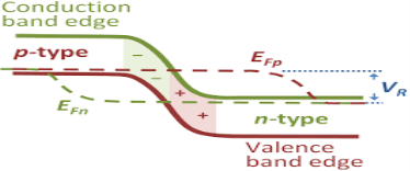
Now for the equation of Fermi we must write down f(E, EFe, T) or f(E, EFh, T) instead of f(E,Ef,T) or E f
.
The carrier concentration of electron or holes in conduction or valance band are as follow
ne = Neffe · [fe in C(E, EFe, T)]Neffe · exp - 
The carrier concentration of electron or holes in conduction or valance band are as follow
ne = Neffn · [fn in C(E, EFn, T)]Neffn · exp - 
This can be cured easily by simply setting 1 – f(E, EFh, T) =: fh in V(E, EFh, T) with fh in V existence the probability of finding holes on the available states in the valence band.
Formally, the electron density in the valence band (EV) then contains 1 – fh in V and so on.
Drift current :-When a vtg is applied to a semiconductor, the free electrons try to drift toward the positive terminal of the battery due to this current flow called drift current.
Diffusion current : In semiconductor it is possible to have a non uniform concentration of charge partials due to non uniform doping
Eg. The concentration of e- on one side of the surface is more than the density on the other side , so the e- will move from the side of greater concentration to the side of lower concentration. This transport of result in to a flow of current which is called diffused current.
The drift current density is given as
J= Jp+Jn
J = q (p p+n
p+n n) E
n) E
Q) Calculate the drift current density in a semiconductor for a given electric field. For germanium sample at T=300oK where ND = 0 and NA =1x1015cm-3ni= 2.4x1013 cm-3. Assume electron and hole mobility to be 3900 cm2/V-sec and 1900 cm2/V-sec. Applied electric field is E= 40V/cm?
Sol: As NA>>ND
p0 = ½ {(NA-ND) + (NA-ND)2+4ni2)1/2}
p0 = 5x1014cm-3
n= ni2/NA
n= 5.76x1011cm-3
J = q (p p+n
p+n n) E
n) E
For extrinsic p-type semiconductor
J = q NA p E =1.6x10-19x1900x1015x40 =12.16 A/cm2
Carrier Lifetime
The time taken by the excess minority carrier to recombine is called as carrier lifetime. There are three methods for recombination mechanism band-to-band, SRH and Ager recombination. SRH is determined by amount of impurities and defects in silicon. Therefore, at high carrier densities, the recombination lifetime in silicon is controlled by Auger recombination and at low carrier densities by SRH recombination.
For SRH recombination the minority carrier life time  n and
n and  p will be
 n =
n = 
 p =
p = 
 ,
,  are fitting parameters
Continuity Equation
The equation shows a change in carrier density over time is due to the difference between the incoming and outgoing flux of carriers plus the generation and minus the recombination.
Consider a small area having flux with infinitesimal amount
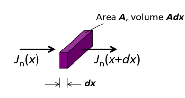


The above equations are called continuity equations.
References
- S. Salivahanan, N. Suresh Kr. & A. Vallavaraj, ―Electronic Devices & Circuit‖, Tata McGraw Hill,
2008
2. Millman, Halkias and Jit, ―Electronic devices and circuits‖ McGraw Hill
3. Boylestad&Nashelsky, ―Electronic Devices & Circuits‖, Pearson Education, 10TH Edition.
4. Sedra& Smith, ―Micro Electronic Circuits‖ Oxford University Press, VI Edition
5. Robert T. Paynter, ―Introducing Electronic Devices & Circuits‖, Pearson Education, VII Edition, 2006